An Efficient Architecture for 'Ifivo-Dimensional Discrete
Wavelet Transform
Po-Cheng Wu and
Liang-Gee
Chen
DSP/IC Design Lab., Department of Electrical EngineeringNational Taiwan University, Taipei, Taiwan, R. 0. C.
Abstract
This paper proposes an efficient architecture for the two- dimensional discrete wavelet transform (2-D DWT). The proposed architecture includes a transform module, a RAM
module, and a multiplexer. In the transform module, we employ the polyphase decomposition technique to the decimation filters of stage 1, and the coe&cient folding technique to the decimation filters of stage 2. The
RAM
size is N/2 x N/2. In comparison with other 2-D DWT architectures, the advantages of the proposed architecture are the near 100% hardware utilization, fast computation time, regular data flow, and low complexity control circuit, making this architecture suitable for next generation image compression systems.I. Introduction
With the rapid progress of VLSI design technologies, many processors based on audio and image signal processing have been developed recently. The tow-dimensional Discrete Wavelet Transform (2-D DWT) is the most important technique of the JPEG-2000 image compression standard [l]. Presently, research on the DWT is attracting a great deal of attention. In addition to audio and image compression, the DWT has important applications in many aspects, such as computer graphics, numerical analysis, radar target distinguishing and so forth. The architecture of the 2-D DWT is mainly composed of the multirate filters. Because an extensive computation is involved in the practical applications, e.g., digital cameras, high efficiency and low cost hardware is indispensable.
At present, many VLSI architectures for the I-D DWT have been proposed. However, for the 2-D DWT, because the filtering operations are required in both the horizontal and vertical directions, designing an efficient architecture with low cost and high throughput is difficult. Lewis and Knowles [2] used the four-tap Daubechies filter to design a 2-D DWT architecture. Parhi and Nishitani [3] proposed two architectures that combine the word-parallel and digital-serial methodologies. Chakrabarti and Vishwanath [4] presented the non-separable architecture and the SIMD array architecture. Vishwanath et al. [ 5 ] employed two systolic array filters and two parallel filters to implement the 2-D DWT. The modified version uses four parallel filters as reported in [ 6 ] and [7]. Chen and Bayoumi [8] presented a scalable systolic array' architecture. Other 2-D DWT architectures have been reported in [9]-[13].
Among the various architectures, the most prevalent design for the 2-D DWT is the parallel filter architecture [ 6 ] , [7]. The design of the parallel filter architecture is based on the Modified Recursive Pyramid Algorithm (MRPA) [4], which intersperses the computation of the second and following levels with the computation of the first level. The MRPA is feasible for the 1-D DWT architecture. However, it is not suitable for the 2-D DWT, because the hardware utilization is inefficient and a complicated control circuit is required due to irregular data flow. Therefore, in this paper, we propose a new VLSI architecture for the 2-D DWT. The advantages of this architecture are the near 100% hardware utilization, fast computation time, regular data flow, and low complexity control circuit. Additionally, the proposed architecture can scale easily with the filter length and the decomposition level.
This paper is organized as follows. In Section 11, an efficient architecture for the 2-D DWT is proposed. Section 111 compares the performance of various 2-D DWT architectures. Finally, conclusions are stated in Section IV.
11. Proposed 2-D
DWT
ArchitectureThe block diagram of the proposed 2-D DWT architecture is shown in Fig. 1. It includes a transform module, a RAM module, and a multiplexer. The size of RAM module is N/2 x 15/2. In the fust level decomposition, the transform module decomposes the input image to four subbands, LL, LH, HL, and HH, and saves the LL band to the RAM. After finishing the first level decomposition, the LL band is sent into the transform module to perform the second level decomposition. This procedure repeats until the desired level J finished.
( L L ~ L L
(LL)'-'LH
,...,
LLLH,LH Input Module (LL)J"HL ,..., LLHL,HL (LL)J"HH,... ,LLHH,HHFig. 1. The proposed 2-D DWT architecture.
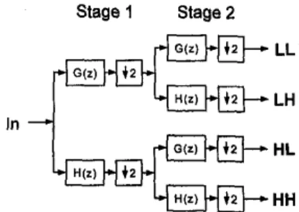
The advantage of such a scheme is that the data flow is very regular. We can concentrate our effort to efficiently design the transform module. As shown in Fig. 2, the transform module is tree-structured and comprises two stages. Stage 1 performs horizontal filtering, and stage 2 performs vertical filtering. To design the transform module efficiently, we assume W ' to be the area cost and ''I" to be the time cost required in stage I . According to the original design as shown in Fig. 2, the number of filters required in stage 2 is double that in stage 1. That is, 2a is the area cost required in stage 2. On the other hand, due to the decimation operation in stage 1, the quantity of data for filtering in each branch of stage 2 is half that of stage 1. Hence, the processing time required in stage 2 is,half of t, i.e., t/2. Because stage 2 is
cascaded after stage 1, stage 2 can not work until stage I
finishes its job. Therefore, from the above discussions we find
that there will be 2a x (t
-
t/2) = at hardware idle in stage 2.In other words, the hardware utilization in the original design of the transform module is inefficient.
Stage 1 Stage 2
.
-HH Fig. 2. The tree-structured transform module.
Table 1. The design strategy of the transform module..
In order to solve this problem, we consider a single decimation filter. The decimation filter can be implemented directly by a filter followed by a two-folded decimator. However, the decimator discards one sample out of every tow samples at the filter output, causing poor hardware utilization. Hence, we employ two different design techniques to enhance its performance. The first technique is the polyphase decomposition technique. It can reduce the time cost from T
to T/2. The second technique is the coefficient folding
technique. It can approximately reduce the area cost from A
to A/2. Now, we employ these two design techniques to the
decimation filters of stage 1 and stage 2, respectively. Therefore, four different design methods are derived for the transform module. The design strategy (including the original design) is listed in Table 1. From Table I, we find that if we employ the polyphase decomposition technique to stage 1 and the coefficient folding technique to stage 2, the area and time cost will both be the same a and t/2 in stages 1 and 2. Thus,
the total area cost is 2a and the total time cost is t/2. The AT
product is reduced from 3at to at, and no hardware is idle in stage 2. It can be seen that the performance of the new design method is three times more efficient than the original design. In contrast, the other design methods, as listed in Table 1, cause the hardware to be idle in stage 2. Hence, they are not efficient design methods.
LL
LH
HL
HH
0
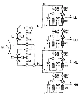
Fig. 3. The transform module employing the polyphase decomposition technique to stage 1 and the coefficient folding technique to stage 2.
Assume that the low-pass filter has four taps: U,, a,, U,, and u3, and the high-pass filter has four taps: bo, b,, b,, and b,. Fig. 3 shows the transform module employing both the polyphase decomposition and the coefficient folding techniques. We have assumed that the filters in stages 1 and 2 have the same length. However, this condition is not necessary for the correct operation in practice. In stage 1, because we use the FIR direct form to implement the polyphase decomposition technique, the low-pass and high- pass decimation filters can share the same registers. In stage 2, because the vertical filtering and the image data are fed by a
raster scan mode, each coefficient requires a line delay to store the row data. The maximum length of the line delay is N/2. Thus, in the first level decomposition, the row data can be stored after horizontal filtering and decimation. In the following decomposition levels, the select signal changes the length of the line delay to N/4, N/8, N/16,
...
, N/2J. The internal clock rate of the transform module is half the input clock rate. When the final data of each level is output, a reset signal is generated to clear the line delay of stage 2, which will prevent the operation of the next level from mixing with the current level.111. Performance Comparisons
The typical 2-D DWT architectures include the parallel filter architecture [7], direct architecture [5], non-separable architecture [4], SIMD architecture [4], and systolic-parallel architecture [5]. In Table 2, we compare the performance of our architecture and these 2-D DWT architectures in terms of the number of multipliers, the number of adders, storage size, computation time, control complexity, and hardware utilization. The computation time has been normalized to the same internal clock rate. The parameter # is the image size, K is the filter length, and J is the decomposition level. The computation time of our architecture is derived as follows:
1 N ’ N’ N ’ N’ 2
T = - ( N ’ +-+--;-+-+...+-) =-(I- 4-”N’
2 4 4 4’ 45.1 3
where the factor 1/2 is due to the fact that the internal clock rate of our architecture is half the input clock rate, Therefore, if our architecture and other architectures have the same internal clock rate, the throughput of our architecture is twice that of other architectures. To do this, doubling the input clock rate for the pixel input can be used. The outcome of the comparisons shows that our design outperforms other architectures, especially in computation time, control complexity, and hardware utilization.
Concerning the storage size, the proposed architecture requires a RAM module of size N/2 x N/2 to save the 114
intermediate data. However, in the 2-D DWT, while dealing with the image that has been stored in memory, e.g., digital
cameras, we can use the same memory to save the pp. 191-202, June 1993.
intermediate data. Therefore, the proposed 2-D DWT [4] C. Chakrabarti and M. Vishwanath, “Eficient realization of architecture will not require the
RAM
module and the value the discrete and continuous wavelet transforms: from single “4 can be discarded in the comparisons. This situation will chip implementations to mappings on SIMD array reduce our storage size substantially. computers,” IEEE Trans. Signal Processing, vol. 43, no. 3, pp.759-771, Mar. 1995.
[3] K. K. Parhi and T. Nishitani, “VLSI architectures for discrete wavelet transforms,” IEEE Trans. VLSI Systems, vol. 1, no. 2,
[SI M. Vishwanath, R. M. Owens, and M. J. Irwin, “VLSI architectures for the discrete wavelet transform,” IEEE Trans. Circuits Syst.-11, vol. 42, no. 5 , pp. 305-316, May 1995. [6] C. Chakrabarti and C. Mumford, “Eficknt realizations of
analysis and synthesis filters based on the 2-D discrete Table 2. The performance comparisons of various 2-D DWT
architectures.
(P:
image size, K filter length, J: decomposition level.)1V.
ConclusionsAt present, many 2-D DWT architectures have been proposed to meet the requirements of real time processing. However, the main problems of these architectures are the inefficient hardware utilization, long computation time, and complicated control circuit. Therefore, in this paper, we propose an efficient 2-D DWT architecture. The proposed architecture has been correctly simulated in the Verilog of CADENCE tool. The advantages of the proposed architecture are the near 100% hardware utilization, fast computation time, regular data flow, and low complexity control circuit, making this design suitable for next generation image compression systems, e.g., JPEG-2000.
References
[l] ISOlIEC JTC 1/SC 29/WG 1 (ITU-T SG8), Coding of Still
Pictures: JPEG 2000 Verification Model Version 3.0 (B). Dec. 1998.
[2] A. S:Lewis and G. Knowles, “VLSI architecture for 2-D Daubechics wavelet transform without multipliers,”
Electronics Letters, vol. 27, no. 2, pp. 171-173, Jan. 1991.
wavelet transform,” in Proc. IEEE Int. ConJ Acoust., Speech, Signal Processing, May 1996, pp. 3256-3259.
[7] C. Chakrabarti and M. Vishwanath, “Architectures for wavelet transforms: A survey,” Journal of VLSI Signal Processing, vol. 14, pp. 171-192, 1996.
[8] Jijun Chen and M. A. Bayoumi, “A scalable systolic array architecture for 2-D discrete wavelet transforms,” in Proc. IEEE VLSI Signal Processing Workshop, 1995, pp. 303-312. [9] R. Rumian, “An architecture for real-time wavelet image
decomposition,” in Proc. IEEE Int. Symp. Circuifs Syst., May 1994, pp. 73-76.
[lo] T. C. Denk and K. K. Parhi, “Calculation of minimum number of registers in 2-D discrete wavelet transforms using lapped block processing,” in Proc. IEEE Int. Symp. Circuits Syst.,
May 1994, pp. 77-81.
[I 11 Henry Y. H. Chuang and Ling Chen, “VLSI architecture far fast 2-D discrete orthonormal wavelet transform,” Journal of
VLSISignal Processing, vol. 10, pp. 225-236, 1995.
[12] J. Bae and V. K. Prasanna, “Synthesis of VLSI architecture for two dimensional discrete wavelet transforms,” in Proc. IEEE Int. ConJ on. Application Specific Array Processors, July
1995, pp. 174-181.
[I31 J. C. Limqueco and M. A. Bayoumi, “A VLSl architecture for separable 2-D discrete wavelet transforms,” Journal of VLSI
SignalProcessing, vol. 18, pp. 125-140, 1998.