Bimodel onset strain relaxation in InAs quantum dots with an InGaAs capping layer
J. F. Chen, Ross C. C. Chen, C. H. Chiang, Y. F. Chen, Y. H. Wu, and L. Chang
Citation: Applied Physics Letters 97, 092110 (2010); doi: 10.1063/1.3483757 View online: http://dx.doi.org/10.1063/1.3483757
View Table of Contents: http://scitation.aip.org/content/aip/journal/apl/97/9?ver=pdfcov Published by the AIP Publishing
Articles you may be interested in
Influence of InGaAs cap layers with different In concentration on the properties of InGaAs quantum dots J. Appl. Phys. 103, 083532 (2008); 10.1063/1.2903143
Photoluminescence linewidths from multiple layers of laterally self-ordered InGaAs quantum dots Appl. Phys. Lett. 87, 213105 (2005); 10.1063/1.2131198
Influences of the spacer layer growth temperature on multilayer InAs GaAs quantum dot structures J. Appl. Phys. 96, 1988 (2004); 10.1063/1.1773378
Effects of a thin InGaAs layer on InAs quantum dots embedded in InAl(Ga)As Appl. Phys. Lett. 83, 3785 (2003); 10.1063/1.1623947
Height-controlled InAs quantum dots by using a thin InGaAs layer Appl. Phys. Lett. 80, 4714 (2002); 10.1063/1.1489484
This article is copyrighted as indicated in the article. Reuse of AIP content is subject to the terms at: http://scitation.aip.org/termsconditions. Downloaded to IP: 140.113.38.11 On: Wed, 30 Apr 2014 10:02:49
Bimodel onset strain relaxation in InAs quantum dots with an InGaAs
capping layer
J. F. Chen,1,a兲Ross C. C. Chen,1C. H. Chiang,1Y. F. Chen,1Y. H. Wu,2and L. Chang2 1Department of Electrophysics, National Chiao Tung University, Hsinchu 30050, Taiwan
2Department of Materials Science and Engineering, National Chiao Tung University,
Hsinchu 30050, Taiwan
共Received 2 June 2010; accepted 7 August 2010; published online 2 September 2010兲
Capping InAs quantum dots 共QDs兲 with an InGaAs layer allows strain relaxation to induce a low-energy electron state below a set of fine dot family states, which is consistent with photoluminescence 共PL兲 spectra. The evolution of InAs thickness suggests a bimodal onset relaxation, i.e., a fine dot family that is strain-relieved by indium outdiffusion from the QDs, as suggested by transmission electron microscopy, and a low-energy dot family that is strain relaxed by the generation of lattice misfits. The indium outdiffusion can explain an abnormal PL blueshift in 70 meV in the fine dot family at onset of strain relaxation. © 2010 American Institute of Physics. 关doi:10.1063/1.3483757兴
Understanding the onset of strain relaxation in InAs self-assembled quantum dots共QDs兲 共Refs.1–16兲 is necessary for designing QD devices.13,14 Strain relaxation in the QDs is accommodated by the generation of threading dislocations in the top GaAs layer and lattice misfits near the front QDs interface,17 suggesting an occurrence of relaxation toward the top GaAs layer. Growing an InGaAs capping layer on top of the QDs leads to strain relaxation by the generation of the lattice misfits in the bottom GaAs layer near the QDs while the top GaAs layer is dislocation-free.18 Thus, the InGaAs capping layer can effectively relieve strain in the top GaAs layer and relaxation occurs toward the bottom GaAs layer with an accompanied photoluminescence 共PL兲 blueshift in about 70 meV.19This blueshift contradicts an effect of com-pressive strain reduction in the QDs, which is expected to produce a redshift. This observation suggests a more compli-cated relaxation than expected. Detailed strain relaxation mechanism has not yet thoroughly established. Therefore, this work describes detailed carrier confinement and PL spec-tra of the InAs QDs with the InAs deposition thickness over a critical relaxation thickness of 3 ML to understand how the strain is relaxed in the InAs QDs.
The InAs QDs were grown by solid source molecular beam epitaxy. On top of a n+-GaAs 共100兲 substrate, a 0.3 m thick Si-doped GaAs 共⬃7⫻1016 cm−3兲 barrier
layer, an InAs layer with deposition thickness from 2 to 3.5 ML was deposited at 490 ° C 共at a rate of 0.26 Å/s兲 to form the QDs. Following the growth of the QDs layer, a 60 Å In0.15Ga0.85As capping layer and a 0.2 m thick Si-doped
GaAs barrier layer were grown to terminate the growth. The QDs were relaxed by increasing the InAs deposition thick-ness slightly above 3 ML, as evident from the induction of lattice misfits18and a PL blueshift about 70 meV.19The QD sheet density was estimated at about 3⫻1010 cm−2. For capacitance-voltage 共C-V兲 profiling, Schottky diodes were realized by evaporating Al with an area of 5⫻10−3 cm2.
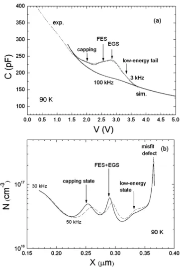
Figure1show the simulated and experimental 90 K C-V spectra共at a low-frequency 3 kHz and a high-frequency 100 kHz兲 and converted experimental electron distribution of a
relaxed InAs QDs diode with the InAs deposition thickness of 3.3 ML. Two major C plateaus are visible at the QD layer: a shallow one from⫺1.5 to ⫺2.2 V, as attributed to a state related to the InGaAs capping layer, and a deep one from
a兲Electronic mail: [email protected].
FIG. 1. 共a兲 90 K experimental and simulated C-V spectra 共at a low-frequency of 3 kHz and a high-low-frequency of 100 kHz兲 and 共b兲 converted electron distribution of a relaxed InAs QDs diode with the InAs thickness of 3.3 ML. The spectra display a shallow capping-layer state, a fine dot family of the FES and EGS, a low-energy tail and a misfit-related defect state.
APPLIED PHYSICS LETTERS 97, 092110共2010兲
0003-6951/2010/97共9兲/092110/3/$30.00 97, 092110-1 © 2010 American Institute of Physics
This article is copyrighted as indicated in the article. Reuse of AIP content is subject to the terms at: http://scitation.aip.org/termsconditions. Downloaded to IP: 140.113.38.11 On: Wed, 30 Apr 2014 10:02:49
⫺2.2 to ⫺3.5 V, as attributed to a fine dot family consisting of electron ground state 共EGS兲 and first excited state 共FES兲, and an additional low-energy tail. Following these two major plateaus is another carrier confinement re-lated to the misfit-rere-lated defect state at 0.35 eV.18 The
experimental carrier distribution in Fig. 1共b兲 clearly reveals the capping-layer state, the fine dot family, the low-energy tail and the misfit defect state. The carrier confinement is analyzed by a C-V simulation based on a similar treatment,20,21 where the low-frequency capacitance is expressed by CL= dQ1+ dQ2/dV=dQ1/dV+dQ2/dV=dV1/
dV/ L1+ dQ2/ dV1dV1/ dV = 共C1+ CQ兲C2 / 共C1+ CQ兲+C2,
where C1=/L1and C2=/L2are the geometric capacitance
per unit area across L1 共distance between the QD layer and the edge of the total depletion width兲 and L2共the depth of the
QD layer兲, and CQ= dQ2/dV1 is the occupied density of
states of the QDs. The confinement energy E 共relative to the GaAs CB edge兲 of the probed QD electrons can be expressed by E = V1+n=共q/2兲ND
⬘
L12+共kT/q兲Ln共NC/ND兲, where Ncisthe effective density of states in the GaAs CB. Additionally, L1 is related to the reverse voltage VR by VR= V1+ V2− Vbi,
where V1=共q/2兲ND
⬘
L12, V2=共q/兲ND⬘
L1L2+共q/2兲NDL22−共L2/A兲兰−⬁E CQdE and Vbi denotes the Schottky barrier
height of the GaAs and A is the area of the diode. According to Fig. 1共a兲, the simulated results 共solid curves兲 correlate well with the experimental data共dotted line兲 by using Gauss-ian distributions CQ共E兲 of a shallow state peaked at 0.09 eV,
a FES at 0.192 eV, a EGS at 0.253, and a long-tail state at 0.30 eV, as shown in Fig.2共a兲. Although a better correlation can be achieved, this work neglects the second-excited state to more clearly visualize other contributions. The fitted E = 0.253 eV for the EGS and the 50 K PL ground emission at 1.074 eV共1.019 eV at 300 K兲 give E of a hole ground state 共HGS兲 of 1.50−1.074−0.253=0.173 eV and a ratio of EGS to HGS of 0.59 to 0.41, a value close to a previously reported 0.61:0.39.21
The fitted carrier distribution in Fig. 2共a兲has a one-to-one correlation with the deconvoluted PL spectra共at 300 K兲 in Fig. 2共b兲, showing a 1.242 eV shallow transition, transi-tions from a fine dot family including the second excited 共SE兲, first excited 共FE兲, and ground 共G兲 states, and an addi-tional 0.948 eV low-energy transition. The FES and EGS have a similar full-width-half-maximum broadness of about 60 meV as the PL broadness of the FE and ground tions. According to our results, the 1.242 eV shallow transi-tion displays a significant redshift with an N incorporatransi-tion into the InGaAs capping layer, and thus is attributed to a
FIG. 2.共a兲 Gaussian electron distributions of a shallow state, FES, EGS, and a long-tail state used for the simulation in Fig.1共a兲. This electron distribu-tion is correlated with the共b兲 300 K PL spectra which show a deconvoluted capping-layer emission, the second-excited, first-excited, ground transitions, and a low-energy transition.
FIG. 3. Evolution of the 50 K PL spectra of the QDs with increasing InAs coverage, under the excitation of 10 mW. For guiding eyes, a dashed line is drawn on the ground transition in the fine dot family. The y-scale is the same for all the spectra.
092110-2 Chen et al. Appl. Phys. Lett. 97, 092110共2010兲
This article is copyrighted as indicated in the article. Reuse of AIP content is subject to the terms at: http://scitation.aip.org/termsconditions. Downloaded to IP: 140.113.38.11 On: Wed, 30 Apr 2014 10:02:49
state belonging to the capping layer. The above results indi-cate that onset of strain relaxation does not degrade the fea-ture of the QDs: it displays a fine dot family similar to that observed in nonrelaxed QDs. Onset of strain relaxation mainly induces a low-energy state.
To illustrate the evolution of strain relaxation, Fig. 3 shows the 50 K PL spectra of the InAs QDs with an increas-ing InAs coverage, under the excitation of 10 mW. A dashed line is drawn to guide the ground emissions from the fine dot family. At the initial formation of the QDs at 2.0 ML, the PL spectra are broad due to large dot-size dispersion at the initial stage. Increasing the InAs coverage increases the dot size and causes a redshift in the ground emission to a maximum of ⬃1250 nm 共⬃1300 nm at 300 K兲 at 2.7 ML. The DLTS measurements reveal no defect signals, indicating coherent QD formation. However, when the InAs coverage is in-creased over a critical thickness of 3 ML to 3.1 ML, the fine dot family still maintains but undergoes an abnormal blue-shift in about 70 meV, in addition to the emergence of a low-energy state 共at ⬃1250 nm兲. When the temperature is lowered 共from 300 to 50 K兲, the low-energy state increases its PL intensity by only a factor of 2, relative to an improve-ment of a factor of ten in the fine dot family. Because PL can be degraded by defects through which photogenerated carri-ers are recombined, the low-energy state is ascribed to a degraded dot family due to the misfit defect state at 0.35 eV.18This finding suggests a nonuniform strain relaxation: a family of dislocated dots and a fine dot family less affected by misfit defects, as evaluated from its fine, well-resolved emissions that are stronger and sharper than that of the 2 ML nonrelaxed dots.
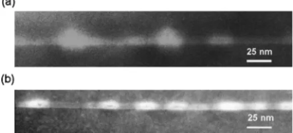
The blueshift in 70 meV observed in the fine dot family contradicts to the strain relaxation in the QDs because the reduction in a compressive strain in the QDs is expected to increase the lattice constant perpendicular to the growth di-rection and extend the emission wavelength. Thus, this blue-shift cannot be explained by the generation of lattice misfits. The TEM image of the relaxed 3.1 ML coverage, as shown in Fig. 4共a兲, leads us to attribute the blueshift to indium outdiffusion from the QDs, in which apparent brightness around the tops of some dots and emanated into the top GaAs layer can be seen, in relation to the TEM image of the nonrelaxed 2.7 ML QDs in Fig. 4共b兲. Previous studies have observed strain related indium segregation.22,23 This indium outdiffusion can cause a PL blueshift as postgrowth thermal annealing. Thus, the built-in strain in the fine dot family is
mainly relieved by the migration of indium adatoms to the top GaAs layer, leading to a reduction in the indium content in the dots and the correlated 70 meV blueshift. According to the results of Fourier transformed TEM images, the dots without the brightness in Fig. 4共a兲display significant lattice misfits inside and near the dots. Thus, we attribute these dots to the family of the dislocated dots. A compressive strain reduction in the QDs can produce a low-energy transition. This bimodal relaxation is probably related to the InGaAs capping layer. Without the capping layer, strain relaxation occurs when the QD deposition thickness is increased to 2.8 ML by the generation of threading dislocation in the top GaAs layer and lattice misfits near the QD top boundary, leading to degraded electronic and PL spectra of the QDs without the blueshift.17
The authors would like to thank the National Science Council of the Republic of China, Taiwan 共Contract No. NSC-97-2112-M-009-014-MY3兲 and MOE ATU program for financially supporting this research. Dr. J. Y. Chi and R. S. Hsiao are commended for preparing the samples.
1F. Heinrichsdorff, M. H. Mao, N. Kirstaedter, A. Krost, and D. Bimberg,
Appl. Phys. Lett. 71, 22共1997兲.
2D. J. Eaglesham and M. Cerullo,Phys. Rev. Lett. 64, 1943共1990兲. 3D. Leonard, K. Pond, and P. M. Petroff,Phys. Rev. B 50, 11687共1994兲. 4J. M. Moison, F. Houzay, F. Barthe, and L. Leprince,Appl. Phys. Lett.64,
196共1994兲.
5C. W. Snyder, J. F. Mansfield, and B. G. Orr,Phys. Rev. B 46, 9551 共1992兲.
6H. Shoji, K. Mukai, N. Ohtsuka, M. Sugawara, T. Uchida, and H. Ish-ikawa,IEEE Photonics Technol. Lett. 7, 1385共1995兲.
7G. Yusa and H. Sakaki,Electron. Lett. 32, 491共1996兲.
8J. C. Campbell, D. L. Huffaker, H. Deng, and D. G. Deppe,Electron. Lett.
33, 1337共1997兲.
9C. M. A. Kapteyn, F. Heinrichsdorff, O. Stier, R. Heitz, M. Grundmann, and P. Werner,Phys. Rev. B 60, 14265共1999兲.
10P. N. Brunkov, A. Patane, A. Levin, L. Eaves, P. C. Main, Y. G. Musikhin, B. V. Volovik, A. E. Zhukov, V. M. Ustinov, and S. G. Konnikov,Phys. Rev. B 65, 085326共2002兲.
11W. H. Chang, W. Y. Chen, T. M. Hsu, N. T. Yeh, and J. I. Chyi,Phys. Rev.
B 66, 195337共2002兲.
12X. Letartre, D. Stievenard, and M. Lanoo,J. Appl. Phys.69, 7336共1991兲. 13H. Drexler, D. Leonard, W. Hansen, J. P. Kotthaus, and P. M. Petroff,
Phys. Rev. Lett. 73, 2252共1994兲.
14S. Sauvage, P. Boucaud, F. H. Julien, J.-M. Gerard, and J.-Y. Marzin,J.
Appl. Phys. 82, 3396共1997兲.
15H. L. Wang, F. H. Yang, S. L. Feng, H. J. Zhu, D. Ning, H. Wang, and X. D. Wang,Phys. Rev. 61, 5530共2000兲.
16J. F. Chen, R. S. Hsiao, C. K. Wang, J. S. Wang, and J. Y. Chi,J. Appl.
Phys. 98, 013716共2005兲.
17J. F. Chen, R. S. Hsiao, W. D. Huang, Y. H. Wu, L. Chang, J. S. Wang, and J. Y. Chi,Appl. Phys. Lett. 88, 233113共2006兲.
18J. F. Chen, Y. Z. Wang, C. H. Chiang, R. S. Hsiao, Y. H. Wu, L. Chang, J. S. Wang, T. W. Chi, and J. Y. Chi,Nanotechnology 18, 355401共2007兲.
19J. F. Chen, R. S. Hsiao, Y. P. Chen, J. S. Wang, and J. Y. Chi,Appl. Phys.
Lett. 87, 141911共2005兲.
20J. F. Chen, N. C. Chen, J. S. Wang, and Y. F. Chen,IEEE Trans. Electron
Devices 48, 204共2001兲.
21S. D. Lin, V. V. IIchenko, V. V. Marin, K. Y. Panarian, A. A. Buyanin, and O. V. Tretyak,Appl. Phys. Lett. 93, 103103共2008兲.
22M. O. Lipinski, H. Schuler, O. G. Schmidt, K. Eberl, and N. Y. Jin-Phillipp,Appl. Phys. Lett. 77, 1789共2000兲.
23J. G. Garcı´a, J. P. Silveira, and F. Briones, Appl. Phys. Lett. 77, 409 共2000兲.
FIG. 4. TEM images of共a兲 the relaxed 3.1 ML coverage and 共b兲 nonrelaxed 2.7 ML coverage. In the relaxed QDs, bright color emanating out of some QDs can be seen, suggesting indium outdiffusion from the QDs.
092110-3 Chen et al. Appl. Phys. Lett. 97, 092110共2010兲
This article is copyrighted as indicated in the article. Reuse of AIP content is subject to the terms at: http://scitation.aip.org/termsconditions. Downloaded to IP: 140.113.38.11 On: Wed, 30 Apr 2014 10:02:49