國 立 交 通 大 學
光 電 系 統 研 究 所
碩 士 論 文
利用埋入式次波長奈米結構提升非晶矽太陽能電池光捕捉效率
Enhanced Light Trapping in Thin Film a-Si Solar Cell by
Embedded Front Pre-patterned Substrate
研究生:韓皓惟
.指導教授:郭浩中教授
林建中教授
利用埋入式次波長奈米結構提升非晶矽太陽能電池光捕捉效率
Enhanced Light Trapping in Thin Film a-Si Solar Cell by
Embedded Front Pre-patterned Substrate
研究生:韓皓惟 Student:Hao-Wei Han
指導教授:郭浩中 教授 Advisor:Hao-Chung Kao
林建中 教授 Chien-Chung Lin
國 立 交 通 大 學
光 電 系 統 研 究 所
碩 士 論 文
A ThesisSubmitted to Institute of Photonic System College of Photonics
National Chiao Tung University in Partial Fulfillment of the Requirements
for the Degree of Master
In
Photonic System
July 2011
Tainan, Taiwan, Republic of China
i
利用埋入式次波長奈米結構提升非晶矽太陽能電池光捕捉效率
研究生:韓皓惟 指導教授:郭浩中、林建中
國立交通大學光電系統所
論文摘要
隨著矽原料的短缺及降低成本的的考量,矽薄膜太陽能電池日益受到重視,但也由 於材料厚度的減少,吸收效率隨之下降,其中更以紅外波段影響甚大,因此如何有效的 增加光在矽材料中的光學路徑,實為矽薄膜太陽能電池之重要課題。 傳統上的光捕捉結構主要是製做於元件的背面,只能藉由繞射或散射增加通過主動 層而還沒有被完全吸收的光線之光學路徑長,但這樣的光捕捉結構往往就沒有抗反射效 果。在本論文中,我們試圖利用一個結構應用於非晶矽太陽能電池之上,能有效增加非 晶矽太陽能電池元件的光電流以及光電轉換效率。我們採用旋塗法搭配奈微米球微影術 這種大面積、便宜又快速的方法,加上非等向性蝕刻達到控制次波長形貌的效果,在事 先沈積在玻璃透明基板上的氮化矽薄膜蝕刻出蛋型次波長奈米結構,再於其上利用真空 濺鍍系統、高密度電漿化學氣相沈積系統、以及電子槍金屬蒸鍍系統依序沈積透明導電 層、非晶矽主動層、和金屬背反射層,而製作出位於入光面且埋入非晶矽主動層的奈米 結構,來同時達到抗反射和光捕捉的效果。 我們可經由積分球吸收頻譜的量測而明確的看見結構所帶來的優異的抗反射和光 捕捉效果,甚至在光線大角度入射元件時,奈米結構依然可以提供更勝於傳統多層膜抗 反射層的表現。短路電流密度可有效的大幅增加,進而將元件光電轉換效率由原本的 5.36%提升至 8.38%。最後我們還利用三維的嚴格耦合波分析(rigorous coupled wave analysis)模擬軟體進行結構的最佳化,進一步預測在製程可行的範圍內,不同的結構 寬度及高度對元件吸收及產生之光電流密度的模擬,可由此得知往後實際實驗的方向, 並減少製程上不必要的測試與時間。ii
Enhanced Light Trapping in Thin Film a-Si Solar Cell by Embedded
Front Pre-patterned Substrate
Student: Hao-Wei Han Advisors: Prof. H. C. Kuo, Prof. C. C. Lin
Institute of Photonic System, National Chiao Tung University
ABSTRACT
Light trapping in amorphous silicon thin film solar cells has been an intensive study
owing to the low absorption coefficient in near-infrared. We demonstrate a frontal
pre-patterned substrate (PPS) on amorphous silicon solar cells, utilizing scalable colloidal
lithography, to serve both functions of anti-reflection at short wavelength and light trapping
effect at long wavelength. We measured the absorption spectrum by an integrating sphere at
normal incidence and the external quantum efficiency (EQE) of three type structures. The
power conversion efficiency of the pre-patterned cell is measured 8.38%, which shows
56.34% and 8.83% enhancement compared to the reference cell with a flat substrate and the
commercialized Asahi U-type substrate, respectively. The increased efficiency is mainly
resulted from the enhanced short-circuit current density (from 12.89 mA/cm2 to 19.77
mA/cm2).
Moreover, the angle-resolved absorption spectroscopy shows superior optical coupling to
the absorber layer at large angles of incidence (AOIs), which guarantees sufficient light
harvesting for the entire day. We also present a design optimization of frontal pre-patterned
substrate with broadband antireflective subwavelength structures based on the theoretical
calculation using a three-dimensional rigorous coupled wave analysis (RCWA) method. The
best structure on our pre-patterned substrate is 500 nm bottom width and 400~450 nm height
iii
Acknowledgements
時間過得真快,碩士班的兩年匆匆過去,回想這兩年來的點點滴滴彷彿一切都在昨 天,好像大家才很生澀地踏進這生活兩年的實驗室怎麼突然又要跟大家分別。在這短暫 的兩年中,參予了實驗室許多大大小小的活動,一路上也受到很多人的幫助,今天才能 對實驗室有一點貢獻完成這一篇的碩士論文。很高興兩年前的選擇是正確的,有幸加入 交大光電所的半導體雷射實驗室,首先當然要感謝我的兩位指導教授-郭浩中老師以及 林建中老師,在實驗上盡其所能地給予協助以及提供豐富的研究資源,在郭老師的督促 與指導下讓我在待人處事與個人發展上都受益良多,而和藹可親且學識淵博的林老師在 我需要協助時所給予的幫助讓我難以忘懷。並且感謝口試委員余沛慈老師以及賴芳儀老 師對我論文的建議與指教,在口試時的寶貴建議讓我的論文能夠更加嚴謹及完整。 感謝我們太陽能組的兩位領導學長-蔡閔安學長以及曾斌誠(Micheal)學長,在這兩 年的碩士班期間一路伴著我成長,實驗上的困難或是模擬的問題總是不厭其煩的教導我。 永遠充滿活力且活蹦亂跳的閔安學長在我遇到困難時總能給我一個樂觀的方向去嘗試, 能想出許多千奇百怪的方法去解決,但做實驗時卻又能拿出身為物理博士的嚴謹與態度, 在問題處理以及領導能力上讓我著實獲益良多。理論及語言能力超強的 Micheal 學長在 我對模擬有問題的任何時候去找他,他都能鉅細靡遺的告訴我所有過程的來龍去脈,喜 歡思考的個性讓他在實驗上能夠提出許多獨到的見解,是我在實驗上學習的楷模。另外 還要感謝信助學長以及珣彣學姊,有著一顆真誠的心的信助不時給我許多鼓勵與加油, 而愛聊天的珣彣學姊總是在做實驗時跟我分享很多的人生經驗。最後是認識還不到一年 有著深厚的物理背景的祐廣,希望將來我們能一起繼續努力。 再來感謝實驗室的夥伴們:羿蓁、瑋婷、Jolin、大寶、幼齒、阿 PO、家齊、祐國、 小杜、峰瑜、冠霖、KaKa、大頭、SGG、Just、季瑾。謝謝你們大家豐富了我的碩班生 活,給予了我一段從來沒有的多采多姿的求學經歷。我永遠都記得當初我們剛到實驗室 來,大家排排坐在工五 250 公用座位的情形,我們的友情就從那時開始萌芽。無法計數iv 的美食團,一群人騎著摩托車浩浩蕩蕩立志要吃遍全新竹,發掘新竹美食沙漠的綠洲的 夢想。還有趁著實驗閒暇之餘,上山下海走透透一次又一次的出遊,每個景點現在想來 都歷歷在目。人小鬼大、活潑熱情的羿蓁有妳在的地方就會有活動,無論是熬夜打牌還 是促膝長談都少不了妳,總是能沒有距離和我們玩成一團,我碩班兩年的綽號也是因妳 而起,叫久了也是蠻習慣蠻親切的。還有天真善良、文靜可愛的瑋婷,喜歡聽妳分享那 些天馬行空的想法與夢境,和妳相處總不時出現意外卻很可愛的有趣場面,謝謝妳總是 對我非常的信任,看到妳在水中緩慢的前進讓我非常的有成就感。再來是我的好搭擋 Jolin,兩年來多謝你在製程上的幫助,很多的時候我們彼此交換意見,在 meeting 上、 在飯局中、或在夜晚的 H 棚停車場,雖然也會有意見不合的時候,但總是在這樣的摩擦 中才能讓我們的默契越來越好,很高興能和你成為夥伴,希望在接下去的博士班生涯我 們能繼續互相幫助與合作。還有大寶和幼齒兩位哥兒們,雖然平常鬥鬥嘴開開玩笑,但 在需要幫助時總是兩肋插刀讓我印象深刻,且擁有高超的攝影技術為我們兩年的點點滴 滴做了紀錄,真是辛苦你們了。感謝阿 PO 成為我們出團的基本角色之一,雖然常常不 知道你到底有沒有搞清楚狀況,但你總是會參加到底。謝謝家齊不厭其煩的為我們大家 解釋紙牌遊戲的遊戲規則,年紀最輕卻是頭腦最靈活的一員。還有好學生祐國,和你討 論課業上的問題總是很有收穫,英文能力超強也是我的楷模之一。感謝阿莎力且喜歡交 朋友的小杜,出遊時有你在就永遠有歡笑。感謝帥氣的峰瑜,你那爽朗的笑聲有將歡笑 散播給大家的傳染力,在親切的笑容背後卻有著成熟穩重的個性。感謝平日不多話的冠 霖,有著一顆精打細算的頭腦,股票哪天有明牌記得偷偷洩漏給我知道。感謝擁有強烈 卡式風格的 KaKa,慢了好幾拍的反應常常讓我們笑到肚子痛,超隨和的個性讓我們對妳 開玩笑也從來不生氣。接著是 NDL 一哥大頭,超挺朋友的你在我需要實驗上的幫忙時總 是義不容辭。再來是新竹美食通 SGG,對每一間餐廳瞭若指掌讓我這個新竹人也訝異。 還有盧老師愛將 Just,在接下來的博士班生涯裡希望繼續互相協助。最後是不常出現在 實驗室的季瑾,碰面時總會停下腳步跟我聊上兩句,互相交換一下近日的生活。另外還 要特別感謝施懷翔和曹廷耀兩位學弟,在這一年來在實驗與模擬上的幫助,有了你們替 我分擔了不少負擔,也希望你們在接下來的學業研究一切順利。
v
最後要感謝我最親愛的家人,你們的默默付出讓我才能無後顧之憂地完成碩士學業, 你們對我的關心與體貼是我碰到困難時最大的精神支柱,有你們陪伴在我身旁我就是全 世界最幸福最幸運的人,謝謝你們!
vi
Content
摘要
...iAbstract
...iiAcknowledgements
...iiiContent
...viList of Tables
...viiiList of Figures
...ixⅠ. Introduction...1
1.1 The Development of Solar Cells...2
1.2 About Thin Film Solar Cells...5
1.3 Motivation...8
Ⅱ. Basic Theories of Solar Cell...10
2.1 Basic principle of solar cell...10
2.2 The Equivalent Circuit Analysis of The Solar Cell...12
Ⅲ. Experimental and Measuring Instruments...18
3.1 Plasma-enhanced chemical vapor deposition (PECVD)...18
3.2 Scanning electron microscope (SEM)...19
3.3 Transmission electron microscopy (TEM)...20
3.4 Integrating sphere reflectance measurement...21
3.5 Power conversion efficiency measurement...24
vii
Ⅳ. Light Management...27
4.1 Minimizing Reflection...27
4.1.1 Optical properties of semiconductor
...27
4.1.2 Anti-reflection coatings
...29
4.2 Light confinement...33
Ⅴ. RCWA (Rigorous Coupled-Wave Analysis) Method...35
Ⅵ. Application of embedded sub-wavelength substrate on amorphous
silicon thin film solar cell...38
6.1 Fabrication processes...40
6.2 Experimental results and discussions...45
6.2.1 Integrating sphere reflectance measurement
...46
6.2.2 External quantum efficiency measurement
...47
6.2.3 Power conversion efficiency measurement
...49
6.3 Angular absorption...51
6.4 Simulation...51
Ⅶ. Conclusion...54
viii
List of Tables
Table 4.1 Refractive indices of selected semiconductors and AR coat materials...28
ix
List of Figures
Figure 1.1 The energy usage trends in 2000 to 2100. The primary energy is the currently used energy by humans including coals and oils. But in the future, as the reduction of the stock of primary energy is bound to be replaced by green energy. The solar energy used in electricity generation in 2100 will be on the leading energy demand... 2
Figure 1.2 This is the classification of various materials and the efficiency of solar cells under the standard solar simulator irradiation measurement...4
Figure 1.3 (a) Absorption coefficients of a number of different photovoltaic materials. (A derivative of the organic semiconductor polyphenylene vinylene (MDMO-PPV) is included for comparison.); (b) Maximum photon current available from each material under AM1.5 illumination, as a function of film thickness, assuming perfect collection of all photogenerated charges. The saturation photocurrent is a function of band gap. The maximum photocurrent supplied by the Am1.5 spectrum is around 49 mAcm-2...7
Figure 2.1 Structure of the basic components of solar cells...10
Figure 2.2 The diagram of photovoltaic effect...11
Figure 2.3 The electron-hole pairs generated in the depletion layer and separated by the electric-field built-in voltage (Vbi)...11
Figure 2.4 The diagram of solar cell equivalent circuit...12
Figure 2.5 The I-V characteristics with and without illumination...13
Figure 2.6 Effect of increasing series and reducing parallel resistances. In each case the outer curve has Rs = 0 and Rsh = ∞. In each case the effect of the resistances is
to reduce the area of the maximum power rectangle compared to Jsc × Voc...17
Figure 3.1 (a) Schematic diagram of conventional reflectivity measurements. (b) Schematic diagram of Integrating sphere reflectance measurements...22
x
Figure 3.3 Schematic diagram of energy conversion efficiency measurement, including a solar simulator, a Keithley 2400 digital power meter for the measurement of electrical characteristics, and a computer with Labview program to process the measurement data...24
Figure 3.4 The erection diagram of grating-based mono-chrometer for the quantum efficiency...25
Figure 4.1 Single layer anti-reflection coating. When the thickness of the dielectric layer is equal to one quarter wavelength, the incident and reflected waves interfere destructively to cancel out the reflected ray at the outer surface...29
Figure 4.2 Calculated reflectivity of single layer AR coat as function of wavelength at different angles of incidence θ= 0°, 30°, 60°. Notice how the minimum of reflectivity lifts and shifts to shorter wavelengths at wider angles of incidence. Calculated for a 100 nm layer of refractive index on top of a semiconductor of refractive index ns = 3.3...31
Figure 4-3 Calculated reflectivity of double layer AR coat, optimized for 700nm. The reflectivity of a single layer is presented for comparison...32
Figure 4.4 Light trapping structure with a tilted rear surface, illustrating a ‗double bounce‘ light path...34
Figure 5.1 The schematic picture of a simple case in the RCWA method. The light is launched from the superstrate region. The analyzed structure is a grating. In the algorithm of RCWA method, all the periodic structures will be split up many such simple grating forms...35
Figure 6.1 In this study, the process of pre-prepared samples. (a) The silicon nitride (SiNx)
of 500 nm was deposited on a glass substrate by using plasma-enhanced chemical vapor deposition (PECVD). (b) The polystyrene (PS) nanospheres was spun on the surface of the SiNx layer, forming a close-packed monolayer mask,
and then shrink the size of the PS spheres...40
Figure 6.2 The top view SEM images of the closely packed polystyrene nanospheres on the SiNx layer...41
xi
Figure 6.3 The device fabrication process of front pre-pattern substrate a-Si solar cell...42
Figure 6.4 Scanning electron microscopic (SEM) images of the fabricated SiNx nipple arrays: (a) a 45-degree tilted top view and (b) a cross-sectional view...43
Figure 6.5 The cross-sectional TEM image of a fabricated solar cell on the pre-patterned substrate...43
Figure 6.6 SEM image of the Asahi U-type sample...44
Figure 6.7 AFM image of the Asahi U-type sample...44
Figure 6.8 Schematic diagram of the sub-wavelength structure for antireflective by gradient refractive index. When the nano-structures is less than the wavelength of incident light, this anti-reflective nano-structure layer can use spatial gradient structure to achieve the effect of graded refractive index. The structure close to the end of air is a higher air ratio and a low refractive index, but the structure close to the end of structure is a lower air ratio and a high refractive index...45
Figure 6.9 The spectrum of cell absorption at normal incident...46
Figure 6.10 The external quantum efficiency (EQE) of the cell for three type substrates...47
Figure 6.11 The improvement factors of the EQE (ΔEQE) for EBN and Asahi U, (a) between 400 nm and 600 nm, and (b) between 600 nm and 800 nm...48
Figure 6.12 The internal quantum efficiency (IQE) of the cell for three type substrates...49
Figure 6.13 J-V measurements of the flat reference, PPS, and Asahi U cells...50
Figure 6.14 The angle-resolved absorption spectroscopy for the cell with the (a) flat substrate and (b) PSS substrate...51
Figure 6.15 The cross section of simulation model structure and the modulation parameters...52
xii
Figure 6.16 The calculated short-circuit current density enhancement compared to the reference flat cell as a function of the bottom width (W) and height (H) of SiNx nipple pattern...53
1
Ⅰ. Introduction
Since the development of the global environment has passed hundreds of thousands of
years, as technology advances and the development of capacity and population growth,
growing demand for expansion of the Earth's resources. IEA (International Energy Agency,
IEA) mentioned in 2007 and 2030 global energy demand will grow by 1.5% at World Energy
Outlook 2009, while after 2030 the world's electricity demand is expected to increase the rate
of 2.5% per year [1]. Coal is still the main fuel of power generation industry. However, the
one of main cause is derived from the carbon dioxide caused by continued growth in global
carbon dioxide emission. This will certainly lead to a long large-scale climate change. It will
give the irreparable harm to the earth. So, how to effectively reduce carbon dioxide emission
is the common face of the issue.
In this regard, an energy revolution can be expected, and the rise of green energy will
play a big lead of the energy revolution. The green energy is a reusable and less polluting
energy sources, such as wind, solar, geothermal, tidal, etc. Solar energy has a very large
number of sources of supply. Because the sun produces about 1.76 × 10⁵ MW energy per year,
of which 600 MW irradiation on the surface of the earth are available. Its energy is 100,000
times than the global average power. With technological advances, our solar energy use
efficiency is also increased. It is expected for a large proportion in the next available energy
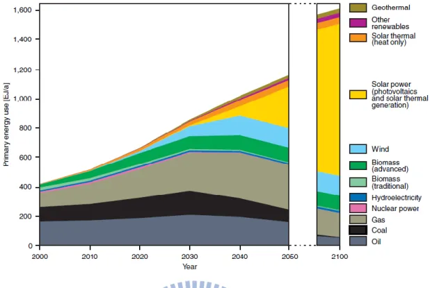
sources account. From Figure 1.1, we can see the future of solar energy usage is expected to
2
Figure 1.1 The energy usage trends in 2000 to 2100. The primary energy is the currently used
energy by humans including coals and oils. But in the future, as the reduction of the stock of
primary energy is bound to be replaced by green energy. The solar energy used in electricity
generation in 2100 will be on the leading energy demand.
1.1 The Development of Solar Cells
The development of the solar cell stems from the work of the French physicist
Antoine-César Becquerel in 1839. Becquerel discovered the photovoltaic effect while
experimenting with a solid electrode in an electrolyte solution; he observed that voltage
developed when light fell upon the electrode. About 50 years later, Charles Fritts constructed
the first true solar cells using junctions formed by coating the semiconductor selenium with an
ultrathin, nearly transparent layer of gold. Fritts's devices were very inefficient, transforming
3
By 1927 another metal-semiconductor-junction solar cell, in this case made of copper
and the semiconductor copper oxide, had been demonstrated. By the 1930s both the selenium
cell and the copper oxide cell were being employed in light-sensitive devices, such as
photometers, for use in photography. These early solar cells, however, still had
energy-conversion efficiencies of less than 1 percent. This impasse was finally overcome with
the development of the silicon solar cell by Russell Ohl in 1941. In 1954, three other
American researchers, G.L. Pearson, Daryl Chapin, and Calvin Fuller, demonstrated a silicon
solar cell capable of a 6-percent energy-conversion efficiency when used in direct sunlight.
By the late 1980s silicon cells, as well as those made of gallium arsenide, with efficiencies of
more than 20 percent had been fabricated. In 1989 a concentrator solar cell, a type of device
in which sunlight is concentrated onto the cell surface by means of lenses, achieved an
efficiency of 37 percent due to the increased intensity of the collected energy. In general, solar
cells of widely varying efficiencies and cost are now available [2]. After the oil crisis, the
most of the world‘s countries alerted the important of new alternative energy development.
The sun is just inexhaustible natural energy, neither energy depletion concerns, but also
avoids the problem of energy monopoly. Therefore, countries actively developed the
application of solar energy technology, expected by increasing the use of solar energy to
reduce dependence on primary energy. The solar cell conversion efficiency research began to
flourish. Today's market-oriented solar cells can be focus on the conversion efficiency of
about range of 10% to 36% [3], while the theoretical maximum efficiency can reach 86% [4].
It can be seen that in the photoelectric conversion efficiency we have a lot of space to develop
these technologies which will be a great help to solve the international community energy
4
Figure 1.2 This is the classification of various materials and the efficiency of solar cells under
the standard solar simulator irradiation measurement.
According to different materials and fabrication process methods can be divided into
different types of solar cells. Material visible on the market today include: silicon materials
(single crystal silicon, polycrystalline silicon, amorphous silicon), III-V semiconductor (GaAs)
materials, II-VI semiconductor (CdS / CdTe) materials and organic materials (TiO2) and so
on. Figure 1.2 is the current solar cell material types and their efficiency comparison chart.
The GaAs solar cells is highest for the current efficiency, its efficiency can be as high as 30%
or more, but it is expensive and containing highly toxic. In the early, it is used on the defense
industry and space satellites, most recently the III-V semiconductor (GaAs) materials has
been used to people‘s livelihood for the high-efficiency concentrator solar power system.
However, the organic solar cells are used in the commercial market yet, but it is really the
5
efficiency of organic solar cells is currently low, but the process is simple, low cost, and has
advantages of transmittance, large area manufacturing and can combine with the flexible
substrate. CIGS solar cell with low cost, long life and high efficiency potential is a lot of
companies to invest in emerging industries, but there is no standardization of products and
technical specifications. The CIGS solar cells used the indium material to fabricate.
According to scholar‘s statistic, the indium material left about 10,000 tons in the whole world.
The next problem that CIGS solar cell has to face is lack of material in the future. Silicon
solar cell technology is currently the most mature and widely applied. There are three types of
silicon solar cells, including single-crystal silicon, polycrystalline silicon, and amorphous
silicon solar cells. And single-crystal silicon and polycrystalline silicon solar cells are
technically more mature and can be mass production.
1.2 About Thin Film Solar Cells
We have seen that , provided that minority carrier diffusion lengths exceed typical
absorption depths, p-n junctions make efficient photoconverters with a high collection
efficiency, where recombination at the surfaces is the dominant loss process. However, single
crystals are expensive to produce and so there is a great deal of interest in finding
photovoltaic materials of less demanding material quality which can be grown more cheaply.
A number of materials have been identified of which the best developed at present are
amorphous silicon (a-Si), polycrystalline cadmium telluride (CdTe), poly-crystalline copper
indium diselenide (CuInSe2) and microcrystalline thin film silicon (μ -Si). These ‗thin film‘
materials are usually produced by physical or chemical deposition techniques which can be
6
Polycrystalline and amorphous semiconductors contain intrinsic defects which increase
the density of traps and recombination centers. For solar cells, this has the consequence that:
Diffusion lengths are shorter, so the material needs to be a strong optical absorber. Alternatively, multiple junctions must be used to make the device optically thick. In the
case of very short diffusion lengths, it may be necessary to use extended built-in electric
field to aid carrier collection. This is the case in amorphous silicon, where p-i-n
structures are preferred.
Losses in the layers close to the front surface are greater, so it is advantageous to replace the emitter with a wider band gap window material.
The presence of defect states in the band gap can make the materials difficult to dope, and limit the built-in bias available from a junction through Fermi level pinning.
The presence of grain boundaries and other intrinsic defects increases the resistivity of the film particularly at low doping densities, and males the conductivity dependent on
the carrier density, so influencing the electrical characteristics of devices.
The presence of defects similarly means that minority carrier lifetime and diffusion constant are carrier density dependent.
Good thin film materials should be low cost, non-toxic, robust and stable [5]. They
should absorb light more strongly than silicon. Higher absorption reduces the cell thickness
and so relaxes the requirement for long minority-carrier diffusion lengths, allowing less pure
polycrystalline or amorphous materials to be used. Figure 1.3 compares the absorption
coefficients for several photovoltaic materials and the maximum photo current which can be
generated in a thin film as a function of its thickness. Notice how weakly crystalline silicon
absorbs, in comparison with the other materials. Suitable materials should transport charge
7
deposited in such a way that arrays of interconnected cells can be produced at once (Figure.
1.3). This greatly reduces the module cost.
Figure 1.3 (a) Absorption coefficients of a number of different photovoltaic materials. (A derivative of the organic semiconductor polyphenylene vinylene (MDMO-PPV) is included for comparison.); (b) Maximum photon current available from each material under AM1.5 illumination, as a function of film thickness, assuming perfect collection of all photogenerated charges. The saturation photocurrent is a function of band gap. The maximum photocurrent supplied by the Am1.5 spectrum is around 49 mAcm-2. [6]
8
Of the elemental semiconductors, only silicon has a suitable band gap for photovoltaic
energy conversion. Compound semiconductors greatly extend the range of available materials
and of these a number of Ⅱ-Ⅵ binary compounds and Ⅰ-Ⅲ-Ⅵ ternary compounds have
been used for thin film photovoltaics. Many of these are direct band gap semiconductors with
high optical absorption relative to silicon. The Ⅰ-Ⅲ-Ⅵ compounds (or chalcogenides) are
analogous to Ⅱ-Ⅵ‘s where the group Ⅱelement has been replaced by a group Ⅰ and a group
Ⅲ species. At present the leading compound semiconductors for thin film photovoltaics are the Ⅱ-Ⅵ semiconductor, CdTe, and the chalcogenide alloys, CuInGaSe2 and CuInSe2. Other
new materials are continually being investigated, including other Ⅱ-Ⅵ and Ⅰ-Ⅲ-Ⅵ
compounds, amorphous carbon and nanocrystalline silicon [6].
1.3 Motivation
To meet the solar cells trend demands ―thin film, high efficiency and low-cost‖,
amorphous silicon solar cell is an excellent choice. Amorphous material has the following
advantages: no restrictions on the supply of materials, production capital is low, with the
prospect of lower production costs, and for the environment and human health effects at a
lower overall total benefits, with the exception of its conversion efficiency is still less than the
current single-crystal silicon and III-V material solar cells. To overcome the lack of efficiency
and cheaper production costs to make the most direct way that is to improve the amorphous
silicon solarcells efficiency of power generation unit. Antireflection layer (AR coating) is
traditionally widely used for various auxiliary structure of solar cells, which allows more
usable light into the active layer of solar cell to be absorbed. In addition, the amorphous
silicon thin-film solar cells are one type of solar cell, the absorption layer thickness of such
9
the light trapping structure we are able to capture light into the active layer of solar cell to stay
longer, and use this way to compensate for the problem of inadequate absorption layer
thickness. In my thesis, we start from these two effects. We use nanosphere lithography
technique to make nano-scale sbuwavelength structure, and we achieve these two effects,
antireflection coating and light trapping, in the same structure simultaneously. As the
perception, Sub-wavelength structures with wide spectrum anti-reflective and light capture
effect can both applied on the amorphous silicon solar cells, it is expected to produce superior
photocurrent and conversion efficiency. In this thesis, we will make out the actual structure,
and use the solar cell efficiency measurement system and the frequency response of the
external quantum efficiency measurement to make the electrical analysis. At the same time in
this thesis, we also use simulation software for rigorous coupled wave analysis (RCWA), and
to study the optical characteristic of nano-structure. The Rigorous Coupled-Wave Analysis
(RCWA) method calculates the diffraction efficiency and field distribution for a 2D or 3D
periodic structure. It helps in the design process of applications such as sub-wavelength
structures, photonic band gap crystals, and other grating-assisted devices. We use this
simulation method to calculate the diffraction efficiency of each diffraction series,
transmittance and other properties, and to simulate the actual experimental results then
combine with the experimental to achieve the optimization of process parameters. It is
accelerated the amorphous silicon thin film solar cells in research and development speed, but
10
Ⅱ. Basic Theories of Solar Cell
2.1 Basic principle of solar cell
Figure 2.1 Structure of the basic components of solar cells[7][8].
The photovoltaic effect is a phenomenon in which electrons are emitted from matter after
the absorption of energy from electromagnetic radiation such as X-rays or visible light. Figure
2.2 shows the diagram of the photovoltaic effect. If the energy of incident light is greater than
or equal to energy gap ( hv ≧ Eg ), electrons could be promoted from ground states to
11
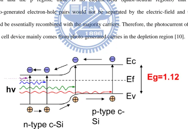
Figure 2.2 The diagram of photovoltaic effect.
The electron-hole pairs generated in the depletion layer are separated by electric-field
built-in voltage (Vbi) and drift to the n-type and p-type region shown in Figure 2.3 [9]. In the n
region and the p region, there is no electric-field (quasi-neutral regions) that the
photo-generated electron-hole pairs would not be separated by the electric-field and they
would be essentially recombined with the majority carriers. Therefore, the photocurrent of the
solar cell device mainly comes from photo-generated carries in the depletion region [10].
Figure 2.3 The electron-hole pairs generated in the depletion layer and separated by the
12
2.2 The Equivalent Circuit Analysis of The Solar Cell
Figure 2.4 The diagram of solar cell equivalent circuit.
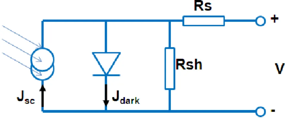
Figure 2.4 illustrates the equivalent circuit of solar cell. From this diagram, one could
find the photo-generated current (I) as follows [11]:
(2-1)
where Isc is the short-circuit current (also called light-generated current, IL), I0 is the reverse
saturation current of the diode, k is the Boltzmann‘s constant, T is the absolute temperature in
degrees Kelvin, n is the ideality factor of diode (1<n<2, n=1 for the Shockley equation), Rs
is the equivalent series resistance and Rsh is the equivalent shunt resistance of the solar cell.
An idealized solar cell, the series resistance Rs is close to infinity and treats as open in the
equivalent circuit. Therefore, the Eq. (2-1) can simplified as:
(2-2)
In Figure 2.4, when the intensity of solar radiation is weak, the current of diode is
approximately the leakage current (
), therefore, Rs can be ignore and Rsh effect is
important, then Eq. (2-1) can be rewritten as:
13
When the intensity of solar radiation is great, the light-generated current is great and
diode is on condition. Therefore, the current of diode is greater than the leakage current
(
), and the Rsh can be ignore and the Rs effect is important. Then the Eq. (2-1) can
be rewritten as:
(2-4)
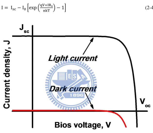
Figure 2.5 The I-V characteristics with and without illumination.
The I-V characteristics of solar cell in dark condition and under illumination were shown
in Figure 2.5 [12]. Four parameters are usually used to characterize the solar cell output
performances and shown in this figure. The parameters used to describe the solar cell
14
(1) Short-Circuit Current, Isc
Isc is determined on the voltage (V) equal to zero by Eq. (2-2). This is equal to the
light-generated current IL ideally. As V=0, the Eq. (2-2) can be written as:
(2-5) (2) Open-Circuit Voltage, Voc
The open-circuit voltage Voc can be solved in I=0 and V=Voc from Eq. (2-2), which is
expressed as:
(2-6) Voc is determined by the properties of the semiconductor by virtue of its dependence on
I0.
(3) Fill Factor, FF
Which is defined as the maximum ratio of the output power to the product on the
short-circuit current and open-circuit voltage, which can be expressed as:
(2-7)
It is measure of how squareness the output characteristics are. For cell of reasonably efficiency, it has a value in the range 0.7 to 0.85.
15
(4) Conversion Efficiency, η
The conversion efficiency of solar cell is defined as the maximum ratio of the output
power to the input power, which can be expressed as
(2-8)
where Pin is the total power under the light incident to the cell.
The solar cell parameters such as open-circuit voltage Voc, short-circuit current Isc and
fill factor FF can provide the information about designing and improving the photodiode due
to their characteristics depended on the properties of the semiconductor materials and the
structure of device.
(5) Quantum Efficiency
Quantum efficiency (QE) is the ratio of the number of charge carriers collected by the
solar cell to the number of photons of a given energy shining on the solar cell. QE therefore
relates to the response of a solar cell to the various wavelengths in the spectrum of light
shining on the cell. The QE is given as a function of either wavelength or energy. If all the
photons of a certain wavelength are absorbed and we collect the resulting minority carriers
(for example, electrons in a p-type material), and then the QE at that particular wavelength
has a value of one. The QE for photons with energy below the bandgap is zero.
The quantum efficiency ideally has a square shape, where the QE value is fairly constant
across the entire spectrum of wavelengths measured. However, the QE for most solar cells is
reduced because of the effects of recombination, where charge carriers are not able to move
into an external circuit. The same mechanisms that affect the collection probability also affect
the QE. For example, modifying the front surface can affect carriers generated near the
16
considerable recombination at the front surface will affect the "blue" portion of the QE.
Similarly, lower energy (green) light is absorbed in the bulk of a solar cell, and a low
diffusion length will affect the collection probability from the solar cell bulk, reducing the QE
in the green portion of the spectrum. In somewhat technical terms, the quantum efficiency can
be viewed as the collection probability due to the generation profile of a single wavelength,
integrated over the device thickness and normalized to the number of incident photons.
"Quantum efficiency" is also sometimes called IPCE, which stands for
Incident-Photon-to-electron Conversion Efficiency.
Two types of quantum efficiency (QE) of a solar cell are often considered:
External Quantum Efficiency (EQE) is the ratio of the number of charge carriers collected by the solar cell to the number of photons of a given energy shining on the solar cell from
outside (incident photons).
Internal Quantum Efficiency (IQE) is the ratio of the number of charge carriers collected by the solar cell to the number of photons of a given energy that shine on the solar cell
from outside and are absorbed by the cell.
The IQE is always larger than the EQE. A low IQE indicates that the active layer of the
solar cell is unable to make good use of the photons. A low EQE can indicate that, but it can
also, instead, indicate that a lot of the light was reflected.
To measure the IQE, one first measures the EQE of the solar device, then measures its
17
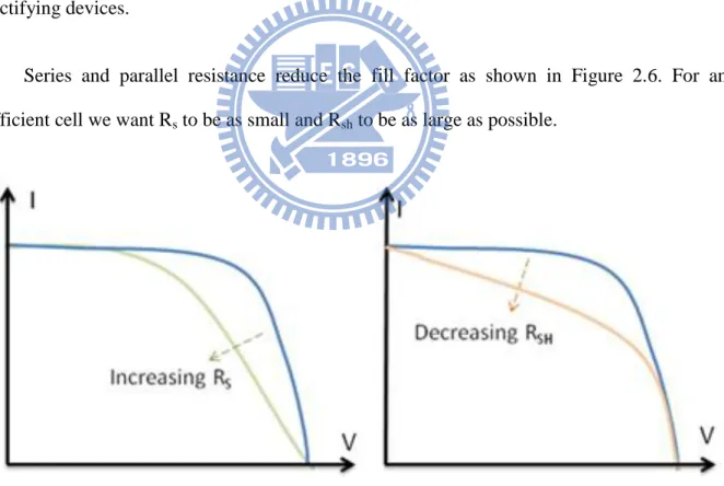
(6) Parasitic Resistances
In real cells power is dissipated through the resistance of the contacts and through
leakage currents around the sides of the device. These effects are equivalent electrically to
two parasitic resistances in series (Rs) and in parallel (Rsh) with the cell (Figure 2.4).
The series resistance arises from the resistance of the cell material to current flow,
particularly through the front surface to the contacts, and from resistive contacts. Series
resistance is a particular problem at high current densities, for instance under concentrated
light. The parallel or shunt resistance arise from leakage of current through the cell, around
the edges of the device and between contacts of different polarity. It is a problem in poorly
rectifying devices.
Series and parallel resistance reduce the fill factor as shown in Figure 2.6. For an
efficient cell we want Rs to be as small and Rsh to be as large as possible.
Figure 2.6 Effect of increasing series and reducing parallel resistances. In each case the outer curve has Rs = 0 and Rsh = ∞. In each case the effect of the resistances is to reduce the area
18
Ⅲ. Experimental and Measuring Instruments
3.1 Plasma-enhanced chemical vapor deposition (PECVD)
Plasma-enhanced chemical vapor deposition (PECVD) is a process used to deposit thin
films from a gas state (vapor) to a solid state on a substrate. Chemical reactions are involved
in the process, which occur after creation of a plasma of the reacting gases. The plasma is
generally created by RF (AC) frequency or DC discharge between two electrodes, the space
between which is filled with the reacting gases.
Plasma deposition is often used in semiconductor manufacturing to deposit films onto
wafers containing metal layers or other temperature-sensitive structures. Silicon dioxide can
be deposited from dichlorosilane or silane and oxygen, typically at pressures from a few
hundred millitorr to a few torr. Plasma-deposited silicon nitride, formed from silane and
ammonia or nitrogen, is also widely used, although it is important to note that it is not
possible to deposit a pure nitride in this fashion. Plasma nitrides always contain a large
amount of hydrogen, which can be bonded to silicon (Si-H) or nitrogen (Si-NH); this
hydrogen has an important influence on UV absorption, stability, mechanical stress, and
electrical conductivity.
Silicon Dioxide can also be deposited from tetraethoxysilane (TEOS) in an oxygen or
oxygen-argon plasma. These films can be contaminated with significant carbon and hydrogen
as silanol, and can be unstable in air. Pressures of a few torr and small electrode spacings,
and/or dual frequency deposition, are helpful to achieve high deposition rates with good film
19
High-density plasma deposition of silicon dioxide from silane and oxygen/argon has
been widely used to create a nearly hydrogen-free film with good conformality over complex
surfaces, the latter resulting from intense ion bombardment and consequent sputtering of the
deposited molecules from vertical onto horizontal surfaces [14].
3.2 Scanning electron microscope (SEM)
A scanning electron microscope (SEM) is a type of electron microscope that images a
sample by scanning it with a high-energy beam of electrons in a raster scan pattern. The
electrons interact with the atoms that make up the sample producing signals that contain
information about the sample's surface topography, composition, and other properties such as
electrical conductivity.
The types of signals produced by an SEM include secondary electrons, back-scattered
electrons (BSE), characteristic X-rays, light (cathodoluminescence), specimen current and
transmitted electrons. Secondary electron detectors are common in all SEMs, but it is rare that
a single machine would have detectors for all possible signals. The signals result from
interactions of the electron beam with atoms at or near the surface of the sample. In the most
common or standard detection mode, secondary electron imaging or SEI, the SEM can
produce very high-resolution images of a sample surface, revealing details less than 1 nm in
size. Due to the very narrow electron beam, SEM micrographs have a large depth of field
yielding a characteristic three-dimensional appearance useful for understanding the surface
structure of a sample. This is exemplified by the micrograph of pollen shown to the right. A
wide range of magnifications is possible, from about 10 times (about equivalent to that of a
20
the best light microscopes. Back-scattered electrons (BSE) are beam electrons that are
reflected from the sample by elastic scattering. BSE are often used in analytical SEM along
with the spectra made from the characteristic X-rays. Because the intensity of the BSE signal
is strongly related to the atomic number (Z) of the specimen, BSE images can provide
information about the distribution of different elements in the sample. For the same reason,
BSE imaging can image colloidal gold immuno-labels of 5 or 10 nm diameter which would
otherwise be difficult or impossible to detect in secondary electron images in biological
specimens. Characteristic X-rays are emitted when the electron beam removes an inner shell
electron from the sample, causing a higher energy electron to fill the shell and release energy.
These characteristic X-rays are used to identify the composition and measure the abundance
of elements in the sample [15].
3.3 Transmission electron microscopy (TEM)
Transmission electron microscopy (TEM) is a microscopy technique whereby a beam of
electrons is transmitted through an ultra thin specimen, interacting with the specimen as it
passes through. An image is formed from the interaction of the electrons transmitted through
the specimen; the image is magnified and focused onto an imaging device, such as a
fluorescent screen, on a layer of photographic film, or to be detected by a sensor such as a
CCD camera.
TEMs are capable of imaging at a significantly higher resolution than light microscopes,
owing to the small de Broglie wavelength of electrons. This enables the instrument's user to
examine fine detail—even as small as a single column of atoms, which is tens of thousands
21
analysis method in a range of scientific fields, in both physical and biological sciences. TEMs
find application in cancer research, virology, materials science as well as pollution,
nanotechnology, and semiconductor research.
At smaller magnifications TEM image contrast is due to absorption of electrons in the
material, due to the thickness and composition of the material. At higher magnifications
complex wave interactions modulate the intensity of the image, requiring expert analysis of
observed images. Alternate modes of use allow for the TEM to observe modulations in
chemical identity, crystal orientation, electronic structure and sample induced electron phase
shift as well as the regular absorption based imaging.
The first TEM was built by Max Knoll and Ernst Ruska in 1931, with this group
developing the first TEM with resolving power greater than that of light in 1933 and the first
commercial TEM in 1939 [16].
3.4 Integrating sphere reflectance measurement
Figure 3.1(A) is a traditional reflectivity measurements diagram. When we want to
measure the reflectance of the smooth surface, the laser light is incident to the sample surface
by a specific angle. As the sample itself is a smooth surface, and the incident light is single
wavelength, we can obtain the reflected light at corresponding angle by the Snell‘s law. At
this point we just put on a light detector on the path of the reflected light, and we can collect
the reflected light from the sample surface effectively. Thus it can measure the reflectance
22
Figure 3.1 (a) Schematic diagram of conventional reflectivity measurements. (b) Schematic
diagram of Integrating sphere reflectance measurements.
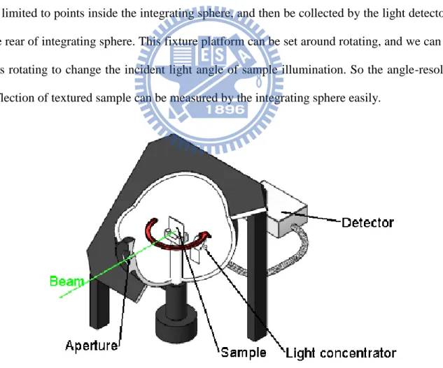
For the particles surface or rough samples, we also want to understand the different
wavelengths light reflectivity, so we change the incident light source to the Xe lamp light with
broadband spectrum. Figure 3.1(b) shows, when we made the surface of the textured structure
which the dimension size is closed to the wavelength of incident light, the different
wavelengths of light on the structure surface produce different levels of splitting, and at the
same time with a large number of light diffraction and scattering phenomenon, which will
make the direction of reflected light is no longer regularly, but from different angles toward
the divergent out. In such condition, if we still use previously measurement way which placed
a light detector in a particular direction, we will only receive a small portion of the reflected
light, so that out of the reflectance measurement is not an objective value. For rough surface
samples, in order to improve the problem of not only received light at a specific point, Fig.
3-1(b), our approach is coupled with an integrating sphere to collect the complete angle
23
sphere and were eventually collected by the light detector. And in order to analyze the
reflectivity of different wavelengths, we require a light detector which can detect wide
spectrum of light. By this way we obtained an objective of the reflectivity data, which
compared to the previous method of measuring reflectivity will be more realistic and accurate.
Figure 3.2 you can see the whole device roughly, we use Xe lamp as the light source to
simulate a wide spectrum of solar incident light, then light pass a convex lens by a guiding
fiber, this allows light to show about horizontal to pass the aperture of the integrating sphere.
The horizontal light pass the aperture of the integrating sphere then illuminate the sample
on the fixture in the integrating sphere. The reflected light is not absorbed by the sample will
be limited to points inside the integrating sphere, and then be collected by the light detector at
the rear of integrating sphere. This fixture platform can be set around rotating, and we can use
this rotating to change the incident light angle of sample illumination. So the angle-resolved
reflection of textured sample can be measured by the integrating sphere easily.
24
3.5 Power conversion efficiency measurement
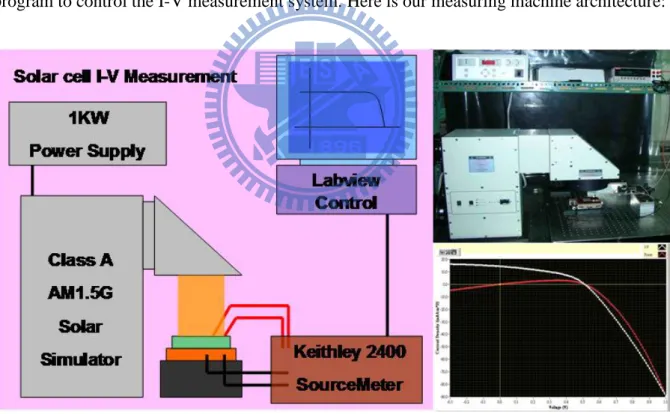
Solar cell device characteristics measurement and analysis in the laboratory, set up by
self-complete measure machine architecture to achieve. We use the U.S. company
manufacturing Newport's AM1.5G 1000W Class A standard solar simulator, the United States
National Renewable Energy Laboratory (NREL) calibrated with international standards set by
the solar spectrum in all bands are within error of only 2%. Before the actual measurement,
using Newport calibration with standard solar cells go after the correction light intensity under
the conditions in 1 sun. We use the temperature controller to maintain the temperature of load
placed at 25℃. And with a Keithley 2400 digital power meter, through a computer Labview
program to control the I-V measurement system. Here is our measuring machine architecture:
Figure 3.3 Schematic diagram of energy conversion efficiency measurement, including a solar
simulator, a Keithley 2400 digital power meter for the measurement of electrical
25
Energy conversion efficiency of solar cells is measured the I-V characteristics under
simulated sunlight illumination conditions (AM1.5G). We can learn about the important
parameters through the conversion efficiency of solar cells, including short-circuit current (Isc),
open-circuit voltage (Voc), fill factor (FF), power conversion efficiency (η ), Maxima power
voltage (Vmax), Maxima power current (Imax), series resistance (Rs), and shunt resistance (Rsh).
3.6 External quantum efficiency measurement
The external quantum efficiency (EQE (λ)), also known as spectral response (SR (λ)), is
very important to understanding the carrier generation, recombination, and diffusion of
photovoltaic devices. External Quantum Efficiency (EQE) is the ratio of the number of charge
carriers collected by the solar cell to the number of photons of a given energy shining on the
solar cell from outside (incident photons). The unit of frequency response is wattage
generated per unit current amperage (A/W), can be converted into quantum efficiency by
under equation:
(3-1)
As under the assumption of the short-circuit point is same the maximum power operating
point, Frequency response measurement is usually measured in the short-circuit conditions.
Solar cell research has developed several sets of external quantum efficiency measurement
system, for example: interference filter and grating-based monochrometer. In terms of single
junction solar cell, single-frequency light generate optical flow into AC voltage signal and
then through the lock-in amplifier to measure. The laboratory uses grating-based
monochrometer system, and its set up as Figure 3.4 [17]. It is applicable to broadband spectral
26
be obtaind by the Xe lamp with broadband spectrum through the grating, and then out from
the slit through the monochrometer focused on the solar cell. The problem of aberration can
be solve by a spherical mirror or a parabolic mirror.
Figure 3.4 The erection diagram of grating-based monochrometer for the quantum efficiency
27
Ⅳ. Light Management
4.1 Minimizing Reflection
4.1.1 Optical properties of semiconductor
The optical properties of a solid are described by the dielectric constant, ε s. ε s is a
complex quality and obeys
(4-1) where ns in the refractive index of the material and the imaginary part ks is related to the
absorption coefficient of the material through
(4-2) In general, ε s, ns and ks are wavelength dependent, and may be direction dependent.
Differences in refractive index determine the reflection and transmission of light at the
interface between two materials. For thin films, light should be treated as coherent, and
Maxwell‘s equations can be solved to find the relative amplitudes of transmitted and reflected
waves. In the simplest case, that of a plane boundary between materials of refractive index n0
and ns, light striking the interface at normal incidence is reflected with probability
(4-3)
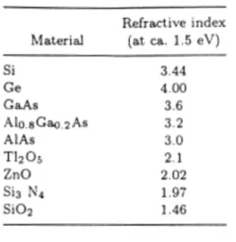
For a semiconductor, ns is typically 3~4 at visible wavelengths (Table 4.1), so that some
28
Table 4.1 Refractive indices of selected semiconductors and AR coat materials.
At oblique incidence the reflectivity is angle and polarization dependent. If the incident
ray makes an angle θ 0 with the surface normal, and the transmitted ray an angle θ s with
the surface normal inside the semiconductor then
(4-4) where
(4-5) for p polarized light (with the electric field vector in the plane of incidence) and
(4-6) and for s-polarized light (electric field vector normal to the plane of incidence). θ 0 and θ s
are related through Snell‘s law
(4-7) For unpolarized light, considered as an equal mix of s and p polarizations, the net
reflectivity generally increases with angle (for the s polarized component it increase while for
the p component it has a minimum), approaching one at large angles. The minimum
reflectivity of a semiconductor surface to unpolarized light occurs at normal incidence and is
given by Eq. 4-3. At 30~40%, this is unacceptably high for efficient photovoltaic energy
29
Snell‘s law also means that travelling within the semiconductor towards the surface at an
angle greater than the critical angle, θ c, is internally reflected. For an air-semiconductor
interface the critical angle is given by
(4-8) For the air-silicon interface θ c = 16.9°. In the presence of an optical coating n0 in Eq.
4-8 is replaced by the refractive index of the coating and θ c is increased.
4.1.2 Anti-reflection coatings
Figure 4.1 Single layer anti-reflection coating. When the thickness of the dielectric layer is
equal to one quarter wavelength, the incident and reflected waves interfere destructively to
cancel out the reflected ray at the outer surface [18-21].
Reflectivity of the air-semiconductor interface can be reduced using an anti-reflection
30
between those of the semiconductor (ns) and free space (n0). By considering forward and
backward travelling waves in each medium it can be shown that the reflectivity of the film for
light of wavelength λ is given by
(4-9)
where δ 1 is the phase shift in the film,
(4-10) θ 1 is the angle between the light ray and the normal within the film, and d1 is the film
thickness. R clearly has its minimum value when δ 1 = π /2. For normal incidence, this first
happens when d1 is equal to a quarter wavelength in the thin film material. (In those
conditions the waves reflected from the front and rear interface of the thin film are out of
phase and interfere destructively.) R vanishes when it is also true that
(4-11)
So by coating our semiconductor with a thin layer of a medium with refractive index
, we can reduce the reflectivity to zero at some particular wavelength, λ 0. Since the solar
spectrum is broad, this wavelength should be chosen to lie towards the middle of range of
wavelengths which can be usefully absorbed for that semiconductor, and this determines the
AR coat thickness. Close to λ 0, R increases with wavelength approximately like
, and
at wavelengths where the phase shift becomes a multiple of π , R reaches its maximum value
equal to the natural reflectivity of the uncoated interface. This means that an AR coat
optimized at one visible wavelength may be quite highly reflecting at others. AR coats on
silicon solar cells are usually optimized for red light, where solar irradiance is strong, and
become reflective in the blue. For this reason silicon solar cells often appear violet or blue.
31
means that AR coats are of limited use in diffuse light or for non-planar surface. Figure 4.2
shows how an AR coat which is tuned for normal incidence at a certain wavelength becomes
reflecting at other wavelengths and angles.
Figure 4.2 Calculated reflectivity of single layer AR coat as function of wavelength at
different angles of incidence θ = 0°, 30°, 60°. Notice how the minimum of reflectivity lifts
and shifts to shorter wavelengths at wider angles of incidence. Calculated for a 100 nm layer
of refractive index on top of a semiconductor of refractive index ns = 3.3.
In the above treatment of AR coats, we neglect the absorption of the optical materials.
This is usually a good approximation since, for most semiconductor, the absorption visible
wavelength is sufficiently weak that . For reflection from an absorbing medium, ns
should properly be replaced by the complex refractive index in Eqs. 4-5~4-9 and R calculated with complex arithmetic. The incident medium should of course be non-absorbing.
32
According to Eq. 4-11, the ideal AR coat material for silicon should have a refractive
index of around 1.84, and for GaAs, 1.90. Good materials are silicon nitride which has n1 =
1.97 and tantalum oxide with n1 = 2.1. These give relectivities of less than 1% at normal
incidence at the optimum wavelength.
Figure 4-3 Calculated reflectivity of double layer AR coat, optimized for 700nm. The
reflectivity of a single layer is presented for comparison.
Improved reflectivity over a band of wavelengths can be achieved with two or more thin
films. The greater the number of layers, the greater the range of wavelengths over which the
reflectivity can be minimized. Multiple layers are not usually practical for solar cells, given
their cost and the sensitivity to angle of incidence, but double layers are used on some hith
efficiency cells. Layers should be deposited so that refractive index increases consecutively
33
when both films have quarter-wave thickness and
(4-12)
This condition allows a little more flexibility in choice of materials than the single layer
case. In some cell designs, where a wide band gap window layer is present for improved
carrier collection, a double layer AR coat can be made simply by choosing an optical coating
with refractive index n1 satisfying Eq. 4-12 where n2 is the refractive index of the window
layer, and choosing appropriate thicknesses. This has been done with GaAs devices having a
high aluminium content AlGaAs window. [6]
4.2 Light confinement
In contrast to anti-reflection coats, which increase the fraction of photons admitted to the
cell, and concentration which increase the incident flux, light confinement techniques increase
the path length of photons inside the cell, once admitted. Increasing the path length increases
the probability of photogeneration per incident photon, particularly when the absorption
coefficient is small, increasing the absorbed fraction. Light trapping is normally considered in
the regime of geometrical optics where structures are large compared to the coherence length
of the light, and light rays with different history do not interfere. This is a good approximation
in silicon where cells are hundreds of microns thick. In micron scale structures, light should
be treated as coherent and interference becomes important. In such systems, classical ray
tracing approaches are not valid, and the photogeneration rate must be found from the
34
The simplest light trapping scheme is to introduce an optical mirror at the rear surface of
the cell, either by metallising the rear cell surface or by growing the active layers on top of a
Bragg stack. The mirror typically reflects over 95% of rays striking the rear surface. Rays
which subsequently reach the front, semiconductor-air, surface are likely to pass through
since the reflectivity of that interface must be small for efficient light capture. So the rear
mirror effectively doubles the path length of the light. For an ideal mirror (with R = 1) and
ideal front surface (with R = 0) the path length is 2w.
The simplest is where one surface is tilted relative to the other. Consider a rear surface
tilted at an angle θ tilt relative to the planar front surface, as in Figure 4.4. When θ tilt >
1/2*θ c, normally incident rays will be reflected from the rear surface at an angle greater than
θ c, and be totally reflected at the front. If a ray strikes the same portion of the rear surface on
the second pass, it will be reflected at an even wider angle, and trapped again. For uniform
cell width, both positive and negative tilt angles must be present, so that trapped rays will
eventually be reflected at narrower angles and escape. If the positive and negative tilt angles
are equal, then each ray makes a multiple of four passes across the cell.
Figure 4.4 Light trapping structure with a tilted rear surface, illustrating a ‗double bounce‘
35
Ⅴ. Rigorous Coupled-Wave Analysis Method
[22]
The diffraction of electromagnetic waves on periodic structures is an important problem
with numerous physical and engineering applications. The core algorithm, which is based on
Rigorous Coupled-Wave Analysis (RCWA), is a rigorous, fully-vectorial solution of
Maxwell's equations [2-2][2-3]. The Rigorous Coupled-Wave Analysis (RCWA) method
calculates the diffraction efficiency and field distribution for a 2D or 3D periodic structure. It
helps in the design process of applications such as sub-wavelength structures, photonic band
gap crystals, and other grating-assisted devices. The RCWA method splits the simulated
structure into several parts with optical properties independent in the main propagation
direction (i.e., the z direction in this study). Figure 5.1 shows a simple case with only one
grating layer. The simulated region is defined by surperstrate, grating, and substrate region.
Figure 5.1 The schematic picture of a simple case in the RCWA method. The light is launched
from the superstrate region. The analyzed structure is a grating. In the algorithm of RCWA
![Figure 2.1 Structure of the basic components of solar cells [7][8].](https://thumb-ap.123doks.com/thumbv2/9libinfo/8242005.171367/24.892.147.797.279.734/figure-structure-basic-components-solar-cells.webp)
![Figure 3.4 The erection diagram of grating-based monochrometer for the quantum efficiency [17]](https://thumb-ap.123doks.com/thumbv2/9libinfo/8242005.171367/40.892.198.748.263.706/figure-erection-diagram-grating-based-monochrometer-quantum-efficiency.webp)