含鉿之閘極介電層於鍺基板之電物性研究
54
0
0
全文
(2) 含鉿之閘極介電層於鍺基板之電物性研究 The Electrical and Material Characterization of Hafnium-family Gate Dielectric on Ge Substrate 研 究 生:鄭 兆 欽. Student:Chao-Ching Cheng. 指導教授:張 俊 彥 博士. Advisor:Dr. Chun-Yen Chang. 國 立 交 通 大 學 電子工程學系 電子研究所碩士班 碩 士 論 文 A Thesis Submitted to Department of Electronics Engineering & Institute of Electronics College of Electrical Engineering and Computer Science National Chiao Tung University in partial Fulfillment of the Requirements for the Degree of Master in Electronics Engineering June 2005 Hsinchu, Taiwan, Republic of China. 中華民國九十四年六月.
(3) 含鉿之閘極介電層於鍺基板之電物性研究 研 究 生:鄭 兆 欽. 指 導 教 授:張 俊 彥 博士. 國立交通大學 電子工程學系. 電子研究所碩士班. 摘. 要. 本論文中,我們有系統地調查各種含金屬鉿之閘極介電材料,包括二 氧化鉿、氮氧化鉿及氮氧化矽鉿,沉積在塊材鍺基板上的電物性研究。 對於鍺晶圓的濕式化學清潔,發現當降低蝕刻酸的濃度時,可以獲得 較平坦的鍺表面,但同時亦會失去恐水性的特性。其中最佳化的清潔方式 為使用稀釋的氫氟酸(氫氟酸:超純水=1:30)與水作循環式交替沖洗,其均方 根表面平整度可達到約 0.133 nm。隨著暴露時間的增加,在鍺表面的原生 氧化層厚度跟碳污染程度均會增高。除此之外,不管是在氬氣或氮氣氣氛 底下,經過五百度熱退火處理後,二氧化鍺的熱脫附現象使得厚度隨著熱 退火時間增加而變薄,這些結果都顯示出二氧化鍺的低熱穩定性將可能造 成高介電金屬氧化物沉積在鍺積板上的後續製程溫度受到限制以及介面受 損的可能性。 由有機金屬化學氣象沉積系統所製備的二氧化鉿薄膜,明顯具有較大 I.
(4) 的等效氧化層厚度及遲滯現象;經過氮氣的沉積後熱退火處理,即使是四 百度的低溫,也會造成電容特性的受損跟漏電流的增加。在沉積二氧化鉿 的過程當中,可以得知較低溫的四百度有利於得到較平整的表面及較小的 電容遲滯,相對地,較高溫的五百度則呈現相反的情況。另外如果預先疊 上金屬鉿(約 10 Å)將更進一步造成等效氧化層厚度下降及遲滯增加,但是這 個現象只有在五百度的沉積溫度才看得到。其次,二氧化鉿介電層可以透 過疊在經過氨氣作氮化處理的鍺表面,獲得更佳的電特性改善。 對於使用濺鍍方式沉積的氮氧化鉿薄膜,隨著熱退火溫度的升高跟時 間的延長,得到的等效氧化層厚度皆會下降,但也同時導致遲滯的增加。 經過六百度五分鐘的熱退火處理,除了等效氧化層厚度可以降低到 19.5 Å, 漏電相較比起標準的二氧化矽/矽結構低了四個數量級。然而不幸地,從介 電層崩潰對時間相依性的可靠度測試中,我們發現十年生命期隨著熱退火 溫度的上升而縮短,推測原因是由於較嚴重的載子捕捉。另一個值得注意 的現象是對於剛沉積的氮化鉿薄膜中,即已經出現了不均勻的氧化,但經 過後續的高溫製程處理將轉變成為均勻的氮氧化鉿薄膜。此時,當熱退火 溫度高於五百度時,我們注意到有大量鍺原子跑入介電層的情況以及氧化 鍺的形成。相信透過製程修正的方式可以持續最佳化其接面結構,進而改 善氮氧化鉿堆疊在鍺基板的電特性表現,使得氮氧化鉿可以成為未來鍺元 件的閘極介電層人選之一。. II.
(5) The Electrical and Material Characterization of Hafnium-family Gate Dielectric on Ge Substrate. Student: Chao-Ching Cheng. Advisor: Dr. Chun-Yen Chang. Department of Electronics Engineering and Institute of Electronics National Chiao Tung University, Hsunchu, Taiwan. ABSTRACT In this thesis, we have systematically investigated the electrical and material characteristics of hafnium-family gate dielectrics, including HfO2, HfOxNy and HfSiON, on bulk Ge substrates. For wet-chemical cleaning of bulk Ge wafers, the flatter surface morphology is observed with decreasing the acid etching concentration, and the hydrophobic phenomenon is simultaneously disappeared. The optimized surface roughness is ~0.113 nm after the cyclical rinse of diluted HF/D.I. water (1:30) and D.I. water. The growth of native oxide and carbon contamination on Ge surface are characterized with increasing the exposure time. Besides, thermal desorption of GeO2 film is observed after 500°C annealing in Ar and N2 ambient. These findings suggest that the limited processing temperature and the interface damage are probable for high-k metal oxides on Ge due to thermal instability of the GeO2. III.
(6) The as-deposited HfO2 thin film prepared by MOCVD shows the large EOT and hysteresis width. After the N2 post-deposition-annealing (PDA), even for low temperature of 400°C, not only the distortion of C-V curves but also the large gate leakage current have been found. During the HfO2 deposition, the low deposition temperature of 400°C facilitates to obtain smoother film, smaller hysteresis but a larger leakage current, while the high deposition temperature of 500°C presents the opposite tendency. Moreover, the Hf pre-deposition (~10 Å) further reveals the EOT and hysteresis damages only for 500°C. The improved electrical properties of the HfO2 dielectrics are seen on NH3-nitrided Ge surfaces. For sputtered HfOxNy thin film, the EOT decreases with increasing the PDA temperature and time, whereas the hysteresis width is increased. A lower EOT of 19.5 Å with the Jg of 1.8 x 10⁻⁵ A/cm2 @ Vg = -1 V, which is ~4 orders reduction as compared to the standard SiO2/Si, has been achieved after 600°C PDA for 5 min. Unfortunately, the 10-year lifetime obtained from the TDDB test is deteriorated with the annealing temperature going up perhaps due to the severe charge trapping. Another noteworthy feature is that the inhomogeneous oxidation of as-deposited HfN film is examined and transferred into the homogeneous HfOxNy film after thermal annealing. Meanwhile, a significant Ge incorporation and the presence of GeOx oxide are also detected upon 500°C. The continuous optimization of the interface structure through process modification has expected to further improve the electrical performance of the HfOxNy/Ge gate stack, which is considered as a candidate for gate dielectric of Ge device.. IV.
(7) 誌. 謝. 在短短兩年的碩士班研究生涯,首先感謝指導教授. 張俊彥 校長,在. 繁忙的校務工作之餘仍耐心地給予實驗室學生們學術上的指導與勉勵,而 老師寬懷的胸襟與遠見更是我們應當學習的目標。其次特別感謝國家奈米 實驗室的. 簡昭欣 博士,其認真的研究態度與豐富的知識,令學生受益匪. 淺。同時亦感謝國家奈米實驗室裡的呂正傑學長、許世祿學長、楊明瑞學 長、黃英傑學長、楊君惠小姐不管在實驗或討論問題上提供了相當大的幫 忙,才得以完成學生的碩士論文。 特別感謝陳經緯學長,在百忙之餘,還時時關心我這個小學弟,也祝 他在未來人生能一切順利平安。另外,包括彭辭修學長、王丁勇學長、陳 怡誠學長、涂峻豪學長、楊宗熺學長及盧文泰學長,感謝他們不僅解答課 業、實驗上的疑問,在日常生活中亦不斷地鼓勵我上進。也謝謝同實驗室 的其他學長及同屆的武陵、道諺、立偉與哲育,還有阿超、耀仁、宗穎、 志偉、文中,陪我一同走過兩年的碩士生活,留下許多快樂的回憶。 接著,我要謝謝小楊老師、舞伴雲雲及社團朋友們,大家可以一起快 樂的跳舞,不僅紓解我實驗上的壓力,也獲得無限多的歡笑。 最後,我要由衷感激親愛的父母,感謝你們辛苦的栽培及默默付出, 使得我得以全心投入學業;謝謝我老哥的打氣跟加油,感謝我最愛的女友 積頤,陪伴我五年之久,給了我無數的支持與鼓勵,永遠愛妳! V.
(8) Contents Abstract (Chinese) --------------------------------------------------------------------Ⅰ Abstract (English) ---------------------------------------------------------------------Ⅲ Acknowledgement ------------------------------------------------------------------ Ⅴ Contents ------------------------------------------------------------------------------ Ⅵ Figure Captions ---------------------------------------------------------------------- Ⅸ. Chapter 1 Introduction 1-1 General Background ----------------------------------------------------------- 1 1-2 Motivation ----------------------------------------------------------------------- 4 1-3 Organization -------------------------------------------------------------------- 6. Chapter 2 The Cleaning Process of Germanium Substrate 2-1 Introduction ------------------------------------------------------------------- 10 2-2 Experimental Procedure ----------------------------------------------------- 11 2-3 Results and Discussion ------------------------------------------------------ 13 2-3-1 Surface morphology of cleaning Ge substrate -------------------- 13 2-3-2 Oxidation and desorption of GeO2 on Ge substrate -------------- 16 2-4 Summary ---------------------------------------------------------------------- 19. VI.
(9) Chapter 3 MOCVD HfO2 Gate Dielectric on Ge Substrate 3-1 Introduction ------------------------------------------------------------------- 37 3-2 Experimental Procedures ---------------------------------------------------- 38 3-3 Electrical and Material Characteristics ------------------------------------ 39 3-3-1 The C-V and I-V characteristics ------------------------------------ 39 3-3-2 High-Resolution Transmission Electron Microscopy and Electron Dispersive Spectra ---------------------------------------------------- 41 3-3-3 Atomic Force Microscopy ------------------------------------------- 42 3-4 Summary ---------------------------------------------------------------------- 43. Chapter 4 Sputtered HfOxNy and HfSiOxNy Gate Dielectric on Ge Substrate 4-1 Introduction ------------------------------------------------------------------- 57 4-2 Experimental Procedures ---------------------------------------------------- 58 4-3 Electrical and Material Characteristics of Pt/HfON/Ge and Pt/HfSiON/Ge MOS Capacitors -------------------------------------------------------------- 59 4-3-1 C-V and I-V characteristics ------------------------------------------ 59 4-3-2 Reliability Issues ----------------------------------------------------- 63 4-3-3 HRTEM and EDS ---------------------------------------------------- 64 4-3-4 XRD、FTIR、AES and XPS -------------------------------------- 65 VII.
(10) 4-4 Summary ---------------------------------------------------------------------- 70. Chapter 5 Conclusions and Suggestions for Future Work 5-1 Conclusions ------------------------------------------------------------------- 99 5-2 Future Work ------------------------------------------------------------------ 101. References ---------------------------------------------------------------------------- 103 Vita ----------------------------------------------------------------------------------- 112. VIII.
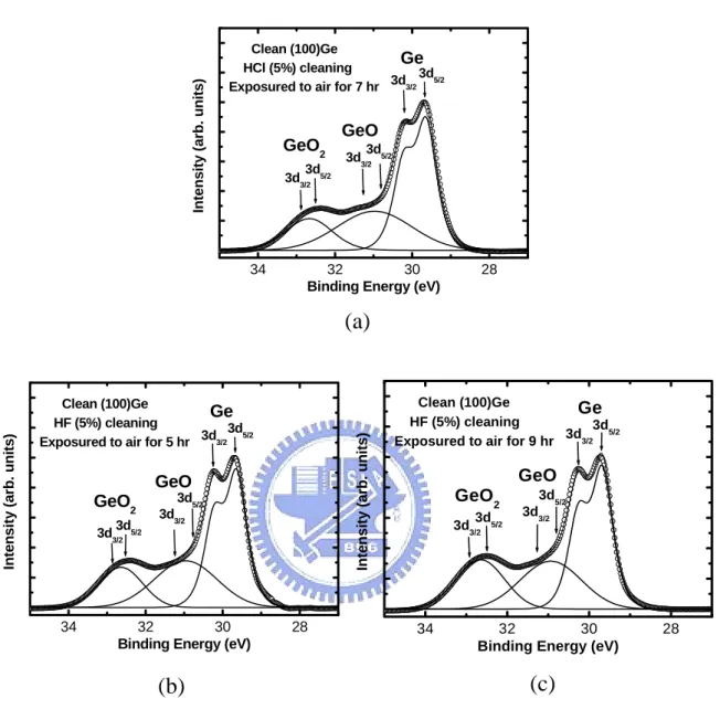
(11) Figure Captions Chapter 1 Introduction Fig. 1-1 The equivalent oxide thickness versus generation nodes for (a) microprocessor, (b) low power. Fig. 1-2 2003 International Technology Roadmap for Semiconductors. Fig. 1-3 Energy gap versus dielectric constant for SiO2, Si3N4, ZrO2, HfO2, ZrSiO4, HfSiO4. Fig. 1-4 Band alignment of typical high-k dielectric materials in contact with Si.. Chapter 2 The Cleaning Process of Germanium Substrate Fig. 2-1 AFM characterization of n-type Ge substrate after different diluted NH4OH cleaning. Fig. 2-2 AFM characterization of n-type Ge substrate after different diluted HF cleaning. Fig. 2-3 AFM characterization of n-type Ge substrate after different diluted HCl cleaning. Fig. 2-4 AFM characterization of p-type Ge substrate after different diluted solution cleaning. Fig. 2-5 The surface roughness of (a) n-type and (b) p-type 4-inch Ge substrate after different diluted solution cleaning. Fig. 2-6 The measured native oxide thickness formed on clean Ge substrate after various exposed time in 10K cleanroom. Fig. 2-7 (a) XPS survey spectra over the binding energy range 0-550 eV, and (b) XPS O 1s core level spectra after different diluted acid solution cleaning. Fig. 2-8 High-resolution XPS spectra of the Ge 3d core level after different diluted acid solution cleaning. (a) exposure time =7 hr after (5%)HCl cleaning. (b) exposure time IX.
(12) =5 hr after (5%)HF cleaning. (c) exposure time =9 hr after (5%)HF cleaning. Fig. 2-9 (a) The fitting results of XPS spectra of Ge 3d core level after the cleaning. (b) The analysis results of XPS spectra of Ge 3d core level after the cleaning. Fig. 2-10 (a) The GeO2 thickness formed by rapid thermal annealing in an O2 ambient. (b) The GeO2 thickness as functions of the temperatures and times. Fig. 2-11 (a) The FTIR spectra of different GeO2 thickness formed by rapid thermal annealing. (b) The correlation between the FTIR spectra and the GeO2 thickness. Fig. 2-12 (a) The FTIR spectra of GeO2 after diluted HF dip or DIW rinse. (b) The GeO2 oxide thickness formed by H2O2 oxidation with and w/o final DI water rinse. Fig. 2-13 (a) The variation of GeO2 thickness after 500°C thermal annealing in an Ar ambient. (b) The variation of GeO2 thickness after 400°C thermal annealing in an Ar ambient. Fig. 2-14 (a) The variation of GeO2 thickness after 500°C thermal annealing in an N2 ambient. (b) The variation of GeO2 thickness after 400°C thermal annealing in an N2 ambient. Fig. 2-15 (a) The FTIR spectra of GeO2 thickness after different thermal desorption in an Ar ambient. (a) The FTIR spectra of GeO2 thickness after different thermal desorption in an N2 ambient. Fig. 2-16 (a) Comparison of the FWHM of GeO2 as a function of the oxidation temperature. (b) Comparison of the FWHM of GeO2 as a function of the oxide thickness. X.
(13) Fig. 2-17 (a) The capacitance-voltage (C-V) characteristics of the Pd/GeO2/n-Ge MOS capacitor. (a) Gate leakage current density (Jg) versus gate voltage (Vg) of the Pd/GeO2/n-Ge MOS capacitor.. Chapter 3 MOCVD HfO2 gate dielectric on Ge substrate Fig. 3-1 (a) The PDA effect on C-V characteristics of Al/HfO2/Ge MOS capacitor w/o surface nitridation. (b) The C-V characteristics of Al/HfO2/Ge MOS capacitor with surface nitridation. Fig. 3-2 (a) The C-V characteristics of Pt/HfO2/Ge MOS capacitor without N2 PDA. The MOCVD HfO2 deposited at 500°C. (b) The C-V characteristics of Pt/HfO2/Ge MOS capacitor with 400℃ N2 PDA. Fig. 3-3 (a)-(d) The C-V characteristics of Pt/HfO2/Ge MOS capacitor with NH3 pre-passivation. The MOCVD HfO2 deposited at 400°C. (e) The effect of NH3 pre-passivation on I-V characteristics of Pt/HfO2/Ge MOS capacitor. Fig. 3-4 (a)-(d) The C-V characteristics of Pt/HfO2/Ge MOS capacitor with and w/o N2 PDA. The MOCVD HfO2 deposited at 350°C. (e) The PDA effect on the I-V characteristics of Pt/HfO2/Ge MOS capacitor. Fig. 3-5 (a)-(c) Temperature-dependent C-V characteristics of Pt/HfO2/Ge MOS capacitor. (d) Temperature-dependent C-V characteristics of Pt/HfO2/Si MOS capacitor. Fig. 3-6 (a) The C-V characteristics of Pt/HfO2/Ge MOS capacitors for different deposition conditions. (b) The hysteresis and gate leakage for different deposition conditions. XI.
(14) Fig. 3-7 The HRTEM images of HfO2 thin film deposited on cleaning Ge substrate (a) No PDA. (b) 500°C PDA. No surface nitridation was done before HfO2 deposition. The deposition temperature for HfO2 dielectric is 500°C. Fig. 3-8 The HRTEM images of HfO2 thin film deposited on nitrided Ge substrate. (a) No PDA. (b) 500°C PDA. Surface NH3 pre-passivation for 5 sec was done before HfO2 deposition. The deposition temperature for HfO2 dielectric is 500°C. Fig. 3-9 The EDS analysis of the compositions of the HfO2 thin film deposited on Ge substrate. The deposition temperature for HfO2 dielectric is 500°C. Fig. 3-10 The HRTEM images of HfO2 thin film deposited on cleaning Ge substrate at different deposition temperatures. (a) 350°C. (b) 400°C. (c) 500°C. Fig. 3-11 The EDS analysis of the compositions of the HfO2 thin film deposited on Ge substrate at different deposition temperatures. (a) 350°C. (b) 400°C. (c) 500°C. Fig. 3-12 AFM characterization of HfO2 thin film on Ge substrate after different PDA temperature annealing. The deposition temperature for HfO2 dielectric is 350°C. Fig. 3-13 AFM characterization of HfO2 thin film on Ge substrate after different PDA temperature annealing. The deposition temperature for HfO2 dielectric is 400°C. Fig. 3-14 AFM characterization of HfO2 thin film on Ge substrate after different PDA temperature annealing. The deposition temperature for HfO2 dielectric is 450°C. Fig. 3-15 AFM characterization of HfO2 thin film on Ge substrate after different PDA temperature annealing. The deposition temperature for HfO2 dielectric is 500°C. XII.
(15) Chapter 4 Sputtered HfOxNy and HfSiOxNy Gate Dielectric on Ge Substrate Fig. 4-1 (a)-(d) Multi-frequency C-V characteristics of Pt/HfOxNy/Ge MOS capacitor before and after the PDA. The sweep direction is from inversion to accumulation. (e) The PDA dependence of frequency dispersion observed in C-V characteristics. Fig. 4-2 (a) The 100 kHz C-V and (b) I-V characteristics of Pt/HfOxNy/Ge (open symbols) MOS capacitors before and after the PDA. For comparison, as-deposited HfOxNy on Si (solid symbols) was also shown. Fig. 4-3 Comparison of (a) the EOT and (b) hysteresis width of the HfOxNy film on Si (solid symbols) and Ge (open symbols) substrates for different PDA temperatures and times. Fig. 4-4 (a) A sequence of 100 kHz C-V curves with various sweep voltage ranges. The inset shows the zoom-in figure. (b) The flatband voltage before and after the PDA extracted from the C-V measurement for Pt/HfOxNy/Ge MOS capacitors. Fig. 4-5 (a) The hysteresis width as a function of sweep voltage range based on VFB for different PDA temperatures. (b) The hysteresis width as a function of sweep voltage range based on VFB for different PDA times. Fig. 4-6 (a) The C-V characteristics of Pt/HfOxNy/Ge MOS capacitor with four sweep voltage ranges. Noted that 600°C annealing was performed for 5 min. The shift of VFB extracted from the sweep direction (b) from inversion to accumulation. (c) from XIII.
(16) accumulation to inversion. Fig. 4-7 (a) The C-V characteristics of Pt/HfOxNy/Ge MOS capacitor with and w/o FGA. (b) The estimated EOT and frequency dispersion as a function of FGA temperature. (c) The Weibull plot shows the FGA effect on EBD. Fig. 4-8 The (a) C-V and (b) I-V characteristics of Pt/HfSiON/p-Ge MOS capacitor before and after the PDA. Fig. 4-9 Gate leakage currents versus the EOT for the deposited HfOxNy and HfSiON films on Ge substrate (solid symbols) were plotted together with other’s published data (open symbols). Fig. 4-10 (a) The Weibull plot shows the effect of PDA temperature on the variation of EBD. (b) The Weibull plot shows the effect of PDA time on the variation of EBD. Fig. 4-11 (a)-(d) The C-V characteristics measured under the CCS of -10-5 A/cm2 for as-deposited and annealed HfOxNy films. (e) The variation of hysteresis width as a function of CCS time for as-deposited and annealed HfOxNy films. Fig. 4-12 (a)-(d) The Weibull plot shows the QBD under three CCS tests for as-deposited and annealed HfOxNy films. (e) The Weibull plot shows the QBD under the CCS of -2x10⁻⁴ A/cm2 for the as-deposited and annealed HfOxNy films. Fig. 4-13 (a)-(d) The Weibull plot shows the TBD under three CVS tests for as-deposited and annealed HfOxNy films. (e) TDDB data reveal the 10-year lifetime extrapolated operating voltage is decreased with PDA temperature. XIV.
(17) Fig. 4-14 (a) The HRTEM images of as-deposited HfOxNy film on Ge and Si substrate. Fig. 4-15 (a) The HRTEM images of as-deposited HfOxNy film on Ge and Si substrate after thermal annealing at 600°C. Fig. 4-16 (a) The HRTEM images of as-deposited HfOxNy film on Ge substrate after post thermal annealing. Fig. 4-17 (a) The EDS spectra of as-deposited HfOxNy film on Ge substrate before and after thermal annealing at 600°C. Fig. 4-18 (a) The EDS spectra of as-deposited HfOxNy film on Si substrate before and after thermal annealing at 600°C. Fig. 4-19 (a) Glancing-angle XRD spectra of HfOxNy deposited film on Ge and Si substrate before and after thermal annealing. (b) The FTIR spectra of HfOxNy deposited film on Ge substrate before and after thermal annealing. Fig. 4-20 (a) The AES depth profiles of as-deposited HfOxNy film on Ge and Si substrate. Fig. 4-21 The AES depth profiles of as-deposited HfOxNy film on Ge substrate before and after the PDA. (a) NKL1. (b) Ratio of N KL1 to OKL1. (c) GeLM2. Fig. 4-22 The universal curve of electron IMFP versus kinetic energy. The inset shows the schematic of XPS incident and emission procedures. Fig. 4-23 Angle-resolved XPS survey from 1200 to 1300 eV for as-deposited and annealed HfOxNy films. (a) Take-off angle = 30°. (b) Take-off angle = 60°. Fig. 4-24 Angle-resolved XPS spectra of as-deposited HfOxNy films w/o PDA. (a) the Hf 4f XV.
(18) core level; (b) the N 1s core level; (c) the O 1s core level. Fig. 4-25 Angle-resolved XPS spectra of the annealed HfOxNy film at 400°C for 5 min. (a) the Hf 4f core level; (b) the N 1s core level; (c) the O 1s core level. Fig. 4-26 Angle-resolved XPS spectra of the annealed HfOxNy film at 500°C for 5 min. (a) the Hf 4f core level; (b) the N 1s core level; (c) the O 1s core level. Fig. 4-27 Angle-resolved XPS spectra of the annealed HfOxNy film at 600°C for 1 min. (a) the Hf 4f core level; (b) the N 1s core level; (c) the O 1s core level. Fig. 4-28 Angle-resolved XPS spectra of the annealed HfOxNy film at 600°C for 5 min. (a) the Hf 4f core level; (b) the N 1s core level; (c) the O 1s core level. Fig. 4-29 Angle-resolved XPS spectra of the Hf 4f core level for the as-deposited and annealed HfOxNy films. (a) Angle = 30°; (b) Angle = 45°; (c) Angle = 60°. Fig. 4-30 Angle-resolved XPS spectra of the N 1s core level for the as-deposited and annealed HfOxNy films. (a) Angle = 30°; (b) Angle = 45°; (c) Angle = 60°. Fig. 4-31 Angle-resolved XPS spectra of the O 1s core level for the as-deposited and annealed HfOxNy films. (a) Angle = 30°; (b) Angle = 45°; (c) Angle = 60°.. XVI.
(19) Chapter 1. Introduction 1-1. General Background The rapid advancement of complementary metal-oxide-semiconductor (CMOS). integrated circuit (IC) technologies in the past few decades has enabled the Si-based microelectronics industry to face several technological challenges. Not only the higher speed, better performance, and huger packing density are pursued, but also less power consumption and lower cost are required. According to the first order current-voltage relationship, the drive current IDS in a MOSFET can be expressed as. I DS =. ⎛ W 1 C OX µ n ⎜ ⎜ L e ff 2 ⎝. ⎞ ⎟⎟ (V G S − V t h ⎠. ). 2. (1.1). Where Cox is the gate oxide capacitance and mainly determined by the permittivity and the thickness of the gate dielectric. Un is the mobility for the electrons or holes, W is the channel width, Leff is the effective channel length, VGS is the applied gate-to-source voltage, and Vth is the threshold voltage. All the parameters in the above formula can be properly adjusted in order to further improve the device driving capability. However, as is well known, large VGS apparently creates an undesirably high electric field across the gate oxide, and the device reliability will be deteriorated in turn. Besides, the reduction of Vth is extremely limited (which is at least ~200 mV) because of the induced statistical fluctuations in thermal energy at. 1.
(20) the normal operation circumstance (~100°C). On the other hand, the shrinkage of the channel length and the increase of gate oxide capacitance are simple and direct methods to achieve the higher driving current and chip density. Thus, the scaling down of Si device’s dimensions is a continuous solution in the past two decades. Up to now, the feature sizes of conventional Si MOSFETs have approximated to its fundamental physical limits. Solely decreasing the channel length and/or the dielectric thickness have not realized the excellent switching ratio, high driving capability, low leakage current and acceptable reliability. Novel device structures and materials are required in order to the further improvement of device performances. Figure 1-1(a) and (b) depict the shrinking trend of gate dielectric thickness as a function of technology node for microprocessor and low-power devices. According to the International Technology Roadmap for Semiconductors (ITRS) 2003 [1], an equivalent oxide thickness (EOT) below 1 nm is specified as one of the aims of sub-0.1 um CMOS devices, as shown in Fig. 1-2. It is well known that since the thickness of conventional SiO2 is less than 1.5 nm, i.e., around three atomic layers in the film, carriers can transport through the gate oxide via direct tunneling and result in the exponential increase of gate leakage current. The resulting gate leakage will increase the power dissipation and deteriorate the device performance as well as the circuit stability for VLSI applications. Therefore, the high dielectric constant (high-k) material must be introduced to replace the conventional SiO2 or oxynitride gate dielectric due to excessive leakage concern and reliability issues. Alternative high-k materials such as Y2O3, TiO2, Al2O3, SrTiO3, ZrO2, HfO2 and their silicates [2-10] have been continually explored. 2.
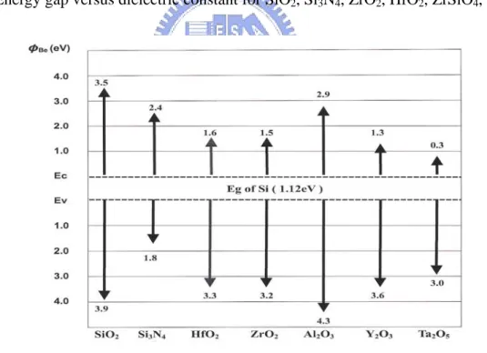
(21) However, a number of candidates, including TiO2 and Ta2O5, require an extra interfacial layer to block significant inter-diffusion and chemical reaction because of the instability of the materials deposited on Si [11, 12]. In addition, high-k material should have a large band-gap, which is inversely proportional to the dielectric constant in most high-k materials, as shown in Fig. 1-3 [13]. The offset of conduction and valance bands in contact with silicon substrate for several high-k gate dielectrics are also shown in Fig. 1-4. Although the leakage current is suppressed for high-k materials due to the thicker physical thickness at the same EOT, the narrower energy gap and smaller band offset will enhance Schottky emission of carriers. Moreover, the trap-assisted tunneling, Frenkel-Poole emission and the hopping effect are also severe compared to silicon dioxide. Thus, there are still several issues for high-k dielectrics before becoming promising candidates in the future, which are shown below: (1) Thermodynamic stability in direct contact with semiconductor substrate. (2) Higher energy band gap with more than 1 eV of conduction band offset to reduce carrier thermal emission. (3) Almost no interfacial layer. (4) Low leakage current ( JG<1 mA/cm2 @ VG-VFB = 1 V). (5) Low interface state density (Dit < 1011 /cm2 eV-1). (6) Hysteresis <20 mV. (7) Amorphous phase of gate dielectric. (8) Good gate compatibility. 3.
(22) (9) Stable process compatibility, especially for the dopant activation of the source/drain. (10) Less mobility degradation. Meanwhile, a higher carrier transport in MOSFETs is also considered through the increase of channel mobility. So far, for enhancing the channel mobility, a strained layer is of interest and has been investigated for a while. Pseudomorphic p-SiGe-channels grown on Si substrates or n-strained-Si on relaxed graded SiGe buffer layers obviously show lower in-plane effective mass for transport and reduce intervalley phonon scattering. Besides, as far as the raise of carrier mobility is concerned, a direct replacement of traditional Si substrate, such as Germanium (Ge) and Ⅲ-Ⅴcompounds, also has been studied a lot. Because of the lower hole and electron effective mass, the hole and electron mobility in Ge are 4x (~1900 cm2/V.s) and 2x (~3900 cm2/V.s), respectively, compared to Si (~450 cm2/V.s and ~1500 cm2/V.s). Naturally, some Ⅲ-Ⅴcompounds provide higher carrier mobility enhancement, but the suitable gate dielectrics is pursued when considering the issues discussed above.. 1-2. Motivation - Why Hafnium-family Gate Dielectric Deposited on Germanium Substrate ? Up to the present, hafnium oxide (HfO2) is the uppermost candidate among all potential. high-k dielectrics due to its relatively large permittivity, reasonably good band offset in contact with silicon substrate [14], and demonstrated compatibility with both poly-silicon [15] and metal gate electrodes [16]. Unfortunately, because of the low crystallization temperature 4.
(23) below 500°C for HfO2, and it become crystallized during the subsequent device processing, which in turn offer extra paths of carriers. In other words, the leakage current increases. The phenomenon of boron penetration in the HfO2 gate dielectric also results in deteriorating the device performance. In addition, the incorporation of Si and/or N into HfO2, i.e., formation of ternary HfON or quaternary HfSiON, have attracted considerable interest due to its several improved features addressing those issues facing binary HfO2, especially for the increase of crystallization temperature and the suppression of phase separation during CMOS processing [17]. However, dielectric constants are reduced in HfSiON due to the presence of silicon oxide bonds with apparently lower dielectric constant than HfO2. According to the report [18], HfSiON with optimized composition ratio remained amorphous state up to 1100°C whereas dielectric constant decreased to ~10. In terms of application, the HfSiON appears to be a very promising material for low power devices rather than for high speed devices due to their EOTs require further scaling-down (< 10 Å) in the near future. On the other hand, HfOxNy seems to be promising for further scaling-down of EOT since incorporated nitrogen strengthen the immunity against oxygen diffusion as well as boron penetration [19] without lowering the dielectric constant. Except the poor interface quality results from the presence of nitrogen, HfOxNy films are expected to have advantages for other essential properties compared to HfO2. HfOxNy has a merit in the thermal stability compared to surface-nitrided and top-nitrided HfO2 because nitrogen bonds exist in the bulk-dielectric as well as at the dielectric/Si interface. Although it crystallizes around ~800°C [20] which is 5.
(24) not high enough to maintain amorphous phase in the conventional self-aligned source/drain process, it provide higher scalability than HfSiON due to its higher dielectric constant. Therefore, it is worth further studying on the electrical and material characteristics of HfOxNy film. As mentioned above, Ge is another great potential semiconductor material because of its higher intrinsic electron and hole mobilities. Together with the lack of sufficiently stable native Ge oxide, this makes the integration of high-k gate dielectric on top of Ge substrate receive more and more attentions. In this article, we integrated the hafnium-based gate dielectrics,. i.e.,. HfO2,. HfOxNy. and. HfSiON,. on. Ge. substrate. to. study. the. metal-oxide-semiconductor characteristics. The differences in the electrical properties have been discussed in relation to material analysis.. 1-3 Organization of the Thesis In Chapter 2, we first developed the cleaning process of Ge substrate. Different diluted solutions were tested for Ge wafer cleaning. Various material analysis techniques, such as Atomic Force Microscopy (AFM), multi-wavelength Ellipsometry, Fourier Transform Infrared Spectrometer (FTIR) and X-ray Photoelectron Spectroscopy (XPS), were performed to observe the surface morphology and surface contamination of Ge substrate after the cleaning procedure. Due to the easily formation of native GeO2 oxide, some material and chemical properties of GeO2 were also described. In Chapter 3, with the optimized cleaning procedure of Ge wafer, the electrical and 6.
(25) material characteristics of MOCVD HfO2 films deposited on clean Ge substrate was discussed. First, the experimental procedure was described, and then the effect of gate electrode was studied. Different deposition conditions, such as deposition temperature, post deposition annealing (PDA) and hafnium precursor pre-deposition, were performed to investigate their effects on HfO2 dielectric properties on the top of Ge wafer. To characterize the material properties and microstructure of the deposited films, High Resolution Transmission Electron Microscopy (HRTEM) and Electron Dispersive Spectra (EDS) were employed. In Chapter 4, the impact of PDA on the electrical and physical characteristics of sputtered HfOxNy and HfSiON thin films on Ge wafer were systemically investigated. Besides, the reliability and charge trapping of Pt/HfOxNy/Ge MOS capacitor after constant current stressing (CCS) and constant voltage stressing (CVS) were also presented. Angle resolved XPS was used to analyze the ~50Å HfOxNy film and interfacial layer (IL) before and after PDA. Glancing angle X-Ray Diffraction (XRD) was taken to examine crystallinity in deposited HfOxNy film after thermal annealing. The correlation between electrical properties and microstructure were established. Finally, Chapter 5 gave the conclusion and suggestions of this thesis for the future works.. 7.
(26) (a). (b). Fig. 1-1 The equivalent oxide thickness versus generation nodes for (a) microprocessor, (b) low power.. ITRS 2003. Fig. 1-2 2003 International Technology Roadmap for Semiconductors. The color shade means the solution known and unknown for physical limit.. 8.
(27) Fig. 1-3 Energy gap versus dielectric constant for SiO2, Si3N4, ZrO2, HfO2, ZrSiO4, HfSiO4.. Fig. 1-4 Band alignment of typical high-k dielectric materials in contact with Si.. 9.
(28) Chapter 2 The Cleaning Process of Germanium Substrate. 2-1 Introduction In the fabrication process of industrial microelectronics, the wafers go through several wet chemical treatments, since it is essential to prepare a clean, defect-free and atomically smooth semiconductor surface for the purpose of studying the surface chemistry and film growth at each stage. Nevertheless, an inhomogeneous layer of amorphous oxide, like native oxide, always formed on the air-exposed surface owing to the presence of unsaturated dangling bonds. For example of the mainstream silicon devices, surfaces terminated by silicon hydride are gaining popularity for the growth of gate oxide, which is used in the fabrication of deep submicron ultra-large integrated circuits. Accordingly, several different methods for Ge surface cleaning have been reported. In the earlier stage, the most common method is ion sputtering with 500-1000 eV Ne+ or Ar+ followed by annealing. Although sputtering is effective in removing surface contamination, the ion-induced damage cannot be completely recovered by annealing alone [21]-[23]. Alternative methods involve wet chemical etching followed by the formation of a passivation layer, then thermal desorption of this layer in an ultrahigh vacuum (UHV) system to leave a clean surface. The most commonly passivation layer is GeO2, which can be prepared by the wet chemical methods [24]-[26], UV-ozone oxidation [27] or a combination of these two [28]. Regardless of how the oxide is formed, 10.
(29) scanning tunneling microscopy (STM) images of surfaces which are prepared by methods mentioned above show trace levels of the protrusions. They are thought to be associated with carbon contamination, which are the most common impurities on Ge surface. This is because not only the lattice mismatch between GeO2 and Ge but the solubility of oxide layer permits some contamination to reach the interface. An alternative method to prepare clean Ge surfaces is to deposit a Ge buffer layer. However, this method has not received as the same attention as either the wet chemical methods or sputter/annealing. For the best of the literatures, only the sulfur- [29] or chlorine-terminated [30] Ge surfaces have been demonstrated to produce an air-stable bulk-like Ge surface, although the applicability of these cleaning solutions for device manufacturing was not be verified yet. In this chapter, we searched some wet chemical treatments, which were tested in our fabrication process, and sought for the optimized cleaning procedures for Ge substrate. Moreover, since the oxidation of semiconductor surfaces are important from both basic and device fabrication technology points of view, thermal oxidation and desorption properties of germanium oxide were also investigated in depth on Ge substrates.. 2-2. Experimental Procedures Both n-type (Sb) and p-type (Ga) doped 4-inch Ge(100) wafers were used in the cleaning. experiments. The resistivity for n-type and p-type wafers were 8-12 and 25-29 Ω .cm, respectively. In this work, only wet chemical treatments were tested in part considering the 11.
(30) usability and feasibility of clean processes in the cleanroom. Firstly the samples were washed with deionized water (DIW) for 5 min. In order to observe the correlation between the surface roughness and cleaning procedures, the samples were subsequently soaked in different diluted solutions for 2 min, which are including NH4OH, HCl and HF, respectively. Various diluted concentrations were prepared to examine their effects. It should be noted that these three solutions are capable of stripping the oxide layer. After removing the native oxide, all samples were rinsed again in DIW for 5 min. The sequence of diluted solution etching and DIW rinse was repeated three times. Eventually, all the samples were dried by dry N2 blowing, and the surface morphology was characterized immediately by atomic force microscopy (AFM). Both X-ray Photoelectron Spectroscopy (XPS) and Fourier Transform Infrared Spectrometer (FTIR) were also employed to measure the surface state of resultant Ge surface. In addition, for evaluating the protective efficiency after the cleaning, the samples were exposed to 10K cleanroom air for periods of time up to two weeks. The formed GeOx thickness was measured by multiple wavelength ellipsometry. On the other hand, some Ge samples after the cleaning process were oxidized to grow the GeO2 oxide by rapid thermal annealing (RTA) system in an O2 ambient. The chamber pressure pumped down to 23 mTorr before the process and kept at 1 atm after the gas stability. Both the temperature and time dependences of GeO2 thickness were investigated. The relation between FTIR spectra and GeO2 thickness was also studied. Most important of all, the temperature dependence of GeO2 layer in an N2 or Ar ambient was investigated to inspect 12.
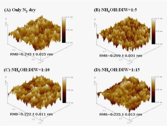
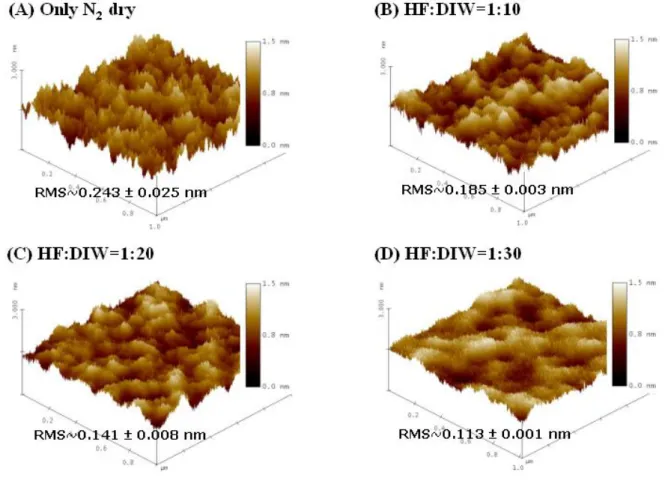
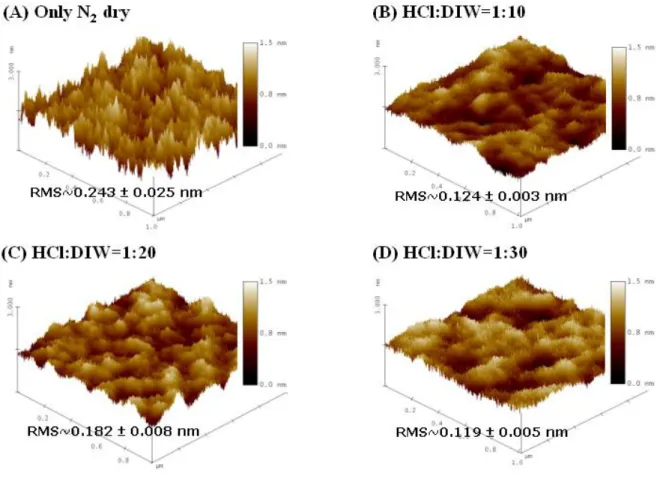
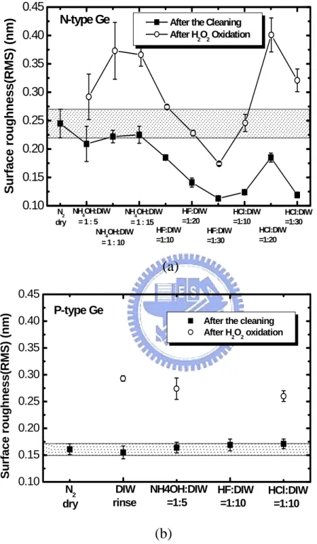
(31) thermal desorption properties. Also, the GeO2 oxide was served as the gate dielectric of MOS capacitors. The 1000 Å Pd was deposited by e-beam evaporation and defined as the capacitor gate electrode by shadow masks. The capacitance−voltage (C−V) and current−voltage (I−V) characteristics were measured by HP4284 LCR meter and Keithley 4200 semiconductor characterization system, respectively.. 2-3. Results and Discussion. 2-3-1 Surface morphology of cleaning Ge substrate Figure 2-1 shows the variation of surface roughness of n-type Ge surface after the cleaning of diluted NH4OH/DIW etching solution with various concentrations of 1:5, 1:10, and 1:15, respectively. The similar surface roughness was found after soaking in NH4OH/DIW solution. According to the report of J. S. Hovis et al. [28], the surface roughness of H2O2-oxidized Ge could be extremely lowered after ammonia etching for 300 sec. It is known that the H2O2 oxidation leads to the obvious increase of surface roughness, which is also consistent with our observation in Fig. 2-5. Hence, in our work, no further improvement after ammonia treatment may be attributed to the absence of H2O2 oxidation in cleaning procedure. However, the roughness of n-type Ge wafer was slightly reduced after the HF/DIW and HCl/DIW cleaning, as shown in Figs. 2-2 and 2-3, respectively. The flatter surface was obtained with decreasing the acid concentration. The optimized surface roughness 13.
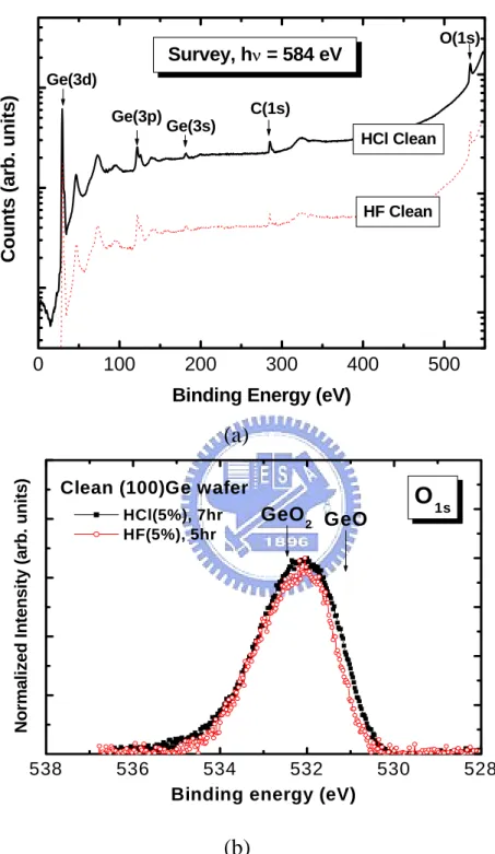
(32) is ~0.113 nm after the cyclical rinse of HF/DIW (1:30) and DIW. It was noteworthy that the HF/H2O (1:100) enables to form the hydrogen-terminated Si surface effectively rather than hydrogen-terminated Ge surface. With the ratio of acid concentration to DIW increasing from 1:30 to 1:10, the hydrophobic phenomenon gradually appeared. Unfortunately, this property still vanished again after the DIW rinse, implying that the lower bond strength of Ge-H surface bonding. On the other hand, as illustrated in Fig. 2-4, the surface morphology seemed to be unchangeable regardless of the clean procedures for p-type Ge wafer. Lower surface roughness is expected to occur if decreasing the concentration of etching solution. All the variation of surface roughness before and after the cleaning is summarized in Fig. 2-5. Noted that because the surface roughness is wafer by wafer, all samples in the experiments come from the same wafer in order to correctly observe the roughness difference. Figure 2-6 plots the detected thickness of GeOx layer on clean Ge substrate after being exposed to 10K cleanroom. Independent of the cleaning processes, the native oxide grew thicker with increasing the exposed time, indicating that the wafers should load into the vacuum chamber as soon as possible after being cleaned. The photoemission experiments were performed at the Synchrotron Radiation Research Center (SRRC) in Hsinchu, Taiwan. Monochromatic radiation was provided by a low-energy spherical grating monochromator (LSGM). Photoelectrons were collected with a 125 mm hemispherical analyzer (Omicron Vakuumphysik GmbH) in a ultrahigh vacuum (UHV) chamber with the base pressure better than 3x10-11 Torr. The binding energies were 14.
(33) referenced to the Au 4f7/2 position at 83.9 eV. After cyclical rinse of diluted acid solution and DIW, the typical XPS survey spectrum with binding energy range of 0-550 eV are displayed in Fig. 2-7(a). Both the C 1s and O 1s signals were detected on clean Ge surface after exposure time of ~6 hr to the air. This result revealed the residual C contamination at the top surface and/or the interface between GeOx and Ge substrate. Furthermore, the peak energies of GeO and GeO2 in O 1s spectrum have been reported to be ~530.8 and ~532.6 eV, respectively [31]. From the Fig. 2-7(b), a broad O 1s band, with the peak energy of ~532 eV, probably corresponded to the combination of these two species. Reasonably, the peak fitting of Ge 3d spectra showed the presence of mainly three components which were elemental Ge, GeO, and GeO2, as also plotted in Fig. 2-8. With respect to pure Ge peak (Ge0+), the higher binding energy is due to GeO, i.e., Gex+ (0<X<4), in a non-bridged configuration, while the highest binding energy component is mainly due to GeO2, i.e., Ge4+ oxidized state, in the form of Ge-O-Ge. All photoelectron peaks were fitted with mixed Lorentzian-Gaussian line shapes after subtraction of the inelastic background intensity. The Ge 3d peak at 29.5 eV is a combination of resolved 3d3/2 and 3d5/2 peaks, which can be decomposed using a spin-orbit splitting of 0.6 eV [32] with an integrated intensity ratio of 2:3 [33]. The fitting results of Ge 3d core-level photoemission spectra are listed in Fig. 2-9(a). Through the comparison of GeO and GeO2 on Ge surface, it showed that the GeOx was the dominant component at initial stage and transformed to the GeO2 with increasing exposure time [34]. Here, the thickness of thin GeOx layer was estimated by using the method 15.
(34) developed for the Si/SiO2 system [35]. The oxide thickness can be expressed as a function of the ratio of Ge 3d integrated areas corresponding to oxide and substrate, namely IGeOx and IGe, respectively. The relation between these parameters is described by the following equation. d. G e O. X. = λ. G e O. X. (s. in α. )ln. ⎛ I G ⎜⎜ I ⎝. e O G e. ∞ G e ∞ G e O. I. X. I. X. ⎞ + 1 ⎟ ⎟ ⎠. (2.1). λ G eO is inelastic mean free path (IMFP) while α is the photoelectron take-off angle. The 2. employed value of I G∞ e / I G∞ e O 2 was 1.30 [36] and the take-off angle was 27o in our work. According to universal curve of IMFP [37]-[39], the photon energy taken in our experiments was 190 eV and corresponded to ~6.5 Å escape depth. The estimated oxide thicknesses for HCl (exposure time = 7 hr), HF (exposure time = 5 hr) and HF (exposure time = 7 hr) are ~2.42, ~2.47 and ~2.56 Å, respectively, which is consistent with ellipsometry measurement.. 2-3-2 Oxidation and desorption of GeO2 on Ge substrate In Fig. 2-10, we investigated temperature and time dependences of the oxide thickness grown by rapid thermal annealing in an O2 ambient. The oxidation rate was linear at initial stage, and for prolonging processing time, the oxidation rate decreased and seemed to evolve towards a parabolic regime, similar to the observations by V. Craciun et al., [36] and Y. Wang et al., [40]. This is in contrast with the logarithmic behavior observed for the lower temperature, 400°C. The more oxidation data should be gathered, including both for the initial and prolonged oxidation time, to clarify these two regimes. From the FTIR spectrum of GeO2 in Fig. 2-11(a), the peaks at 865 and 970 cm-1 coincided to the Ge-O stretching mode, while the broad band between 510 and 590 cm-1 was consistent to the Ge-O bending mode [36, 40]. 16.
(35) As the oxide thickness increased, not only the integrated intensity but also main peak intensity at 865 cm-1 increased linearly. As displayed in Fig. 2-12(a), a ~90 Å oxide was almost dissolved in DIW due to its water-soluble property, and could be completely stripped by diluted HF dip. In addition, Fig.2-12(b) presents the eventual GeO2 thickness after H2O2 oxidation with and without DIW rinse. We observed that the time-independence H2O2 oxidation implied the growth of inhomogeneous GeO2 layer. Due to different oxidation degree on Ge surface, the subsequent annealing desorption will result in the unsmooth surface. Thus, in view of surface uniform, we suggested that the passivation layer oxidized at lower temperature might be considered as a better method with respect to H2O2 oxidation. Besides, H2O2 oxidation with DIW rinse finally, only residual thin oxide was observed, in agreement with the FTIR spectra above. Figures 2-13 and 2-14 show the annealing of GeO2 layer in an Ar or N2 ambient as function of the temperature and the time. It was found that the GeO2 oxide layer shrank at 500°C annealing, while that was stable at 400°C annealing. The desorption rate of GeO2 oxide in an Ar and N2 ambient were almost the same at 500°C. K. Prabhakaran et al., have demonstrated that the GeO2 species transformed to GeO and finally desorb from the Ge surface upon ~425°C [41]. We further compared our FTIR spectra of GeO2 before and after thermal annealing, as illustrated in Fig. 2-15, the closely identical peak intensities were obtained after 400°C annealing, while the diminished peak intensities were observed after 500°C and 600°C annealing. Interestingly, a narrowing of the full width at half maximum 17.
(36) (FWHM) of GeO2 spectrum was only exhibited after 600°C annealing. Due to this unusual feature, we examined again the FWHM of as-oxidized GeO2 as functions of oxidation temperature and thickness, which is shown in Fig. 2-16. By normalizing the peak intensity, the FHWM was found to be almost the same for all oxidation temperatures and thicknesses. Hence, the possible mechanism for FHWM shrinkage is unclear and further investigation is still required. Besides, the C-V and I-V characteristics of Pd/GeO2/Ge MOS capacitor are demonstrated in Fig. 2-17. No frequency dispersion, hump and hysteresis were observed in C-V curves. The equivalent oxide thickness (EOT) evaluated at Vg = 1.5 V is ~110 Å. The dielectric constant is ~3.2 if assuming the physical thickness of ~90 Å. The corresponding gate leakage current density was 6.3 x 10⁻⁹ A/cm2 @ Vg = 1 V. In our work, thermally growth of GeO2 on Ge was performed at 500°C, and the capacitance characteristics were excellent. V. Craciun et al. found that the electrical properties of the GeO2 grown at 350°C were rather poor. The improved C-V and I-V characteristics were observed for the films grown at higher oxidation temperatures, i.e., 450°C [36]. In addition, the inversion capacitance of our C-V curves revealed a significant dependence on the measuring frequency. This fact is partly explained by the fast minority carrier generation in Ge because of its smaller bandgap [42]. It is believed that the bulky defects within the forbidden energy-gap also enhance the generation rate due to the reduced minority carrier lifetime.. 18.
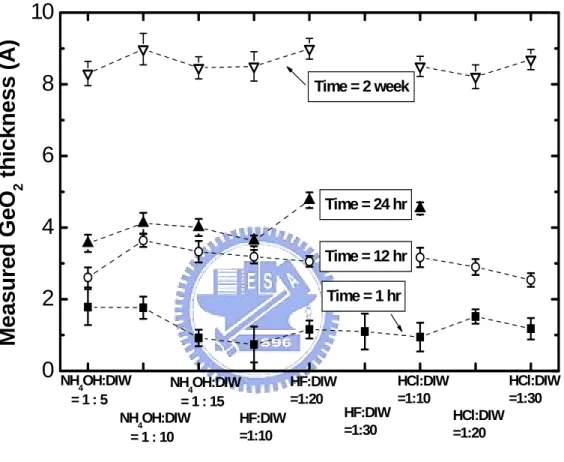
(37) 2-4. Summary In the cleaning procedures, the flatter surface was found with decreasing the acid. concentration, whereas the hydrophobic phenomenon was also vanished. The optimized surface roughness was ~0.113 nm after the cyclical rinse of HF/DIW (1:30) and DIW. From the ellipsometry measurement and XPS examination, it showed that the growth of native oxide as the exposure time increased, and carbon contamination was also detected. The native oxide was estimated about 2-3 Å for exposed time up to 12 hr. The oxidation behavior of Ge substrate showed two regimes, i,e., linear oxidation rate was at initial stage, and the saturated oxidation rate was at prolonged stage. Thermal desorption of GeO2 films also was observed after 500°C annealing in Ar and N2 ambient. Together with the easily oxidized properties of Ge, these experimental findings suggest that post processing temperature chosen shall be lower than 500°C, and 400°C is considered in case of GeO2 existence.. 19.
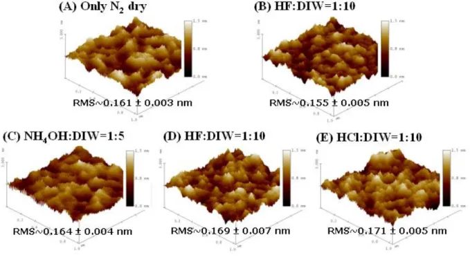
(38) Fig. 2-1 AFM characterization of n-type Ge substrate after different diluted NH4OH cleaning. The scale height is 1.5 nm.. 20.
(39) Fig. 2-2 AFM characterization of n-type Ge substrate after different diluted HF cleaning. The scale height is 1.5 nm.. 21.
(40) Fig. 2-3 AFM characterization of n-type Ge substrate after different diluted HCl cleaning. The scale height is 1.5 nm.. 22.
(41) Fig. 2-4 AFM characterization of p-type Ge substrate after different diluted solution cleaning. The scale height is 1.5 nm.. 23.
(42) Surface roughness(RMS) (nm). 0.45 N-type Ge. After the Cleaning After H2O2 Oxidation. 0.40 0.35 0.30 0.25 0.20 0.15 0.10. HF:DIW NH4OH:DIW N2 NH4OH:DIW HCl:DIW HCl:DIW =1:20 =1:10 =1:30 = 1 : 15 dry = 1 : 5 HCl:DIW HF:DIW HF:DIW NH4OH:DIW =1:20 =1:10 =1:30 = 1 : 10. (a). Surface roughness(RMS) (nm). 0.45 0.40. P-type Ge After the cleaning After H2O2 oxidation. 0.35 0.30 0.25 0.20 0.15 0.10. N2 dry. DIW rinse. NH4OH:DIW HF:DIW =1:5 =1:10. HCl:DIW =1:10. (b) Fig. 2-5 The surface roughness of (a) n-type and (b) p-type 4-inch Ge substrate after different diluted solution cleaning.. 24.
(43) Measured GeO2 thickness (A). 10 8. Time = 2 week. 6 Time = 24 hr. 4 Time = 12 hr. 2. Time = 1 hr. 0 NH OH:DIW. HCl:DIW HCl:DIW HF:DIW NH4OH:DIW =1:30 =1:10 =1:20 =1:5 = 1 : 15 HF:DIW HCl:DIW NH4OH:DIW HF:DIW =1:30 =1:20 =1:10 = 1 : 10 4. Fig. 2-6 The measured native oxide thickness formed on clean Ge substrate after various exposed time in 10K cleanroom.. 25.
(44) O(1s). Survey, hν = 584 eV Counts (arb. units). Ge(3d) Ge(3p). C(1s) Ge(3s). HCl Clean. HF Clean. 0. 100. 200. 300. 400. 500. Binding Energy (eV). Normalized Intensity (arb. units). (a) Clean (100)Ge wafer. 538. 536. O 1s. GeO 2 GeO. HCl(5%), 7hr HF(5%), 5hr. 534 532 Binding energy (eV). 530. 528. (b) Fig. 2-7 (a) XPS survey spectra over the binding energy range 0-550 eV, and (b) XPS O 1s core level spectra after different diluted acid solution cleaning.. 26.
(45) Intensity (arb. units). Clean (100)Ge Ge HCl (5%) cleaning 3d5/2 3d 3/2 Exposured to air for 7 hr. GeO2 3d5/2. GeO 3d 3d3/2 5/2. 3d3/2. 34. 32 30 Binding Energy (eV). 28. Clean (100)Ge Ge HF (5%) cleaning 3d5/2 3d 3/2 Exposured to air for 5 hr. Intensity (arb. units). Intensity (arb. units). (a). GeO GeO2 3d 3d3/2 5/2. 34. 3d5/2. 3d3/2. 32 30 Binding Energy (eV). 28. Clean (100)Ge Ge HF (5%) cleaning 3d 3d3/2 5/2 Exposured to air for 9 hr. GeO GeO2 3d5/2. 3d3/2. 34. 3d5/2 3d3/2. 32 30 Binding Energy (eV). 28. (c). (b). Fig. 2-8 High-resolution XPS spectra of the Ge 3d core level after different diluted acid solution cleaning. (a) exposure time =7 hr after (5%)HCl cleaning. (b) exposure time =5 hr after (5%)HF cleaning. (c) exposure time =9 hr after (5%)HF cleaning. It should be noted that the cleaning procedure is a cyclical rinse of DI wafer and diluted acid solution.. 27.
(46) (a) Intensity Ratio = GeOx / Ge (%). 60. 60. GeOx GeOx. 50. 50. GeO2 GeO2. 40. 40. 30. HCl(5%) 7hr. HF(5%) 5hr. HF(5%) 9hr. Intensity Ratio = GeO2 / Ge (%). 70. 70. 30. (b) Fig. 2-9 (a) The fitting results of XPS spectra of Ge 3d core level after the cleaning. (b) The analysis results of XPS spectra of Ge 3d core level after the cleaning.. 28.
(47) Measured GeO2 thickness (A). 200 160 120 Rapid thermal oxidation o O2 ambient, 500 C, 1atm. 80 40 0. 10 20 30 Oxidation time (min.). 40. Measured GeO2 thickness (A). (a) 100. o. Oxidation Temp.= 500 C o Oxidation Temp.= 400 C o Oxidation Temp.= 350 C. 80. O2 ambient, 1 atm. 60 40 20 0. 0. 1. 2 3 Oxidation time (min.). 4. (b) Fig. 2-10 (a) The GeO2 thickness formed by rapid thermal annealing in an O2 ambient. (b) The GeO2 thickness as functions of the temperatures and times.. 29.
(48) Absorbance (arb. units). Ge - O stretching. O 2 ambient oxidation o Temperature = 500 C Pressure = 1 atm. T OX T OX T OX T OX T OX T OX. Ge - O stretching. ~ 10A ~ 15A ~ 30A ~ 45A ~ 80A ~100A. Ge - O bending. Thickness. 1200. 1000 800 -1 Wavenumber (cm ). 600. Integrated Ge-O stretching intensity -1 Peak height at 865 cm. -1. Peak intensity at 865 cm (arb. units). Integrated spectrum intensity (arb. units). (a). 20. 40 60 80 100 Measured GeO 2 thickness (A). 120. (b) Fig. 2-11 (a) The FTIR spectra of different GeO2 thickness formed by rapid thermal annealing. (b) The correlation between the FTIR spectra and the GeO2 thickness.. 30.
(49) Rapid thermal oxidation. Absorbance (arb. units). Pressure = 1 atm o Temp. = 500 C Time = 3 min Thickness ~ 90 A. Ge - O stretching. GeO 2 DI rinse, 5 min HF dip, 1 min. Ge - O stretching Ge - O bending. 1200. 1000 800 -1 Wavenumber (cm ). 600. Measured GeO2 thickness (A). (a) 50. H 2O 2 oxidation w/o DIW final dip H 2O 2 oxidation with DIW final dip. 40 30 20 10 0. 1. 2 3 4 H 2O2 oxidation time (min.). 5. (b) Fig. 2-12 (a) The FTIR spectra of the GeO2 after diluted HF dip or DI water rinse. (b) The GeO2 thickness formed by H2O2 oxidation with and w/o final DI water rinse.. 31.
(50) Measured GeO2 thickness (A). 120. o. As-oxidized 0.5min, 500 C o As-oxidized 1min, 500 C o As-oxidized 2min, 500 C o As-oxidized 3min, 500 C o As-oxidized 4min, 500 C. o. 500 C, Ar ambient. 100 80 60 40 20 0. native oxide thickness. 0. 5 10 15 Ar desorption time (min.). 20. Measured GeO2 thickness (A). (a) 110. o. 400 C, Ar ambient. 100 o. As-oxidized 3.5min, 400 C o As-oxidized 4min, 400 C o As-oxidized 3min, 500 C. 90. 25 20 15. 0. 5 10 Ar desorption time (min.). 15. (b) Fig. 2-13 (a) The variation of GeO2 thickness after 500℃ thermal annealing in an Ar ambient. (b) The variation of GeO2 thickness after 400℃ thermal annealing in an Ar ambient.. 32.
(51) Measured GeO2 thickness (A). 100. o. 500 C, N2 ambient. o. As-oxidized 1min, 500 C o As-oxidized 2min, 500 C o As-oxidized 3min, 500 C o As-oxidized 4min, 500 C. 80 60 40 20 0. 0. 5 10 15 N2 desorption time (min.). 20. Measured GeO2 thickness (A). (a) 110. o. 400 C, N2 ambient. 100 o. As-oxidized 3.5min, 400 C o As-oxidized 4min, 400 C o As-oxidized 3min, 500 C. 90 30 20 0. 5 10 N2 desorption time (min.). 15. (b) Fig. 2-14 (a) The variation of GeO2 thickness after 500℃ thermal annealing in an N2 ambient. (b) The variation of GeO2 thickness after 400℃ thermal annealing in an N2 ambient.. 33.
(52) Absorbance (arb. units). Rapid thermal oxidation Pressure = 1 atm o Temp. = 500 C Time = 3 min Thickness ~ 100 A. Ge - O stretching. No Annealing o Ar, 400 C, 5 min o Ar, 500 C, 5 min o Ar, 600 C, 5 min. Ge - O stretching Ge - O bending. 1200. 1000. 800. 600 -1. Wavenumber (cm ). (a). Absorbance (arb. units). Rapid thermal oxidation Pressure = 1 atm o Temp. = 500 C Time = 3 min Thickness ~ 110 A. Ge - O stretching. No Annealing o N2, 400 C, 5 min o. N2, 500 C, 5 min o. N2, 600 C, 5 min. Ge - O stretching Ge - O bending. 1200. 1000. 800. 600 -1. Wavenumber (cm ). (b) Fig. 2-15 (a) The FTIR spectra of GeO2 thickness after different thermal desorption in an Ar ambient. (b) The FTIR spectra of GeO2 thickness after different thermal desorption in an N2 ambient.. 34.
(53) Absorbance (arb. units). O2 ambient oxidation. 1.0. Ge - O stretching. Pressure = 1 atm. o. Toxidized = 400 C o. Toxidized = 500 C o. All measured spectra of the different thickness have been normlized to peak-intensity. Toxidized = 600 C. Ge - O stretching. 0.5. Ge - O bending. 0.0. 1200. 1000 800 -1 Wavenumber (cm ). 600. (a) Ge - O stretching. Absorbance (arb. units). O2 ambient oxidation. 1.0. o. Temperature = 500 C Pressure = 1 atm All measured spectra of the different thickness -1 are normlized to 861cm. 0.5. 0.0. Ge - O stretching. 1200. 1000 800 -1 Wavenumber (cm ). TOX ~ 10A TOX ~ 15A TOX ~ 30A TOX ~ 45A TOX ~ 80A TOX ~100A. Ge - O bending. 600. (b) Fig. 2-16 (a) Comparison of the FWHM of GeO2 as a function of the oxidation temperature. (b) Comparison of the FWHM of GeO2 as a function of the oxide thickness.. 35.
(54) 2. Gate Capacitance density (µF/cm ). Pd/GeO2/Ge. 0.3. 0.2 o. 500 C, O2 ambient, 3min 1MHz (acc-to-inv) 1MHz (inv-to-acc) 100kHz (acc-to-inv) 100kHz (inv-to-acc) 10kHz (acc-to-inv) 10kHz (inv-to-acc). 0.1. 0.0 -1.5. -1.0. -0.5. 0.0 0.5 Vg(volts). 1.0. 1.5. 1E-3. 2. 1E-3. Gate leakage current density (A/cm ). (a) Gate leakage current (A). 1E-4. Pd/GeO2/Ge. 1E-5. leakage current. 1E-4. leakage current density. 1E-5 1E-6. 1E-6. -9. 2. Jleak@1V ~ 6.3x10 A/cm. 1E-7. 1E-7. 1E-8. 1E-8. 1E-9. 1E-9. 1E-10. 1E-10. 1E-11. 1E-11. 1E-12. 1E-12. 1E-13. 1E-13 1E-14. 1E-14 -1. 0. 1. Vg(volts). (b) Fig. 2-17 (a) The C-V characteristics of the Pd/GeO2/n-Ge MOS capacitor. (a) The gate leakage current versus gate voltage of the Pd/GeO2/n-Ge MOS capacitor.. 36.
(55)
數據

+7
相關文件
You are given the wavelength and total energy of a light pulse and asked to find the number of photons it
Reading Task 6: Genre Structure and Language Features. • Now let’s look at how language features (e.g. sentence patterns) are connected to the structure
In BHJ solar cells using P3HT:PCBM, adjustment of surface energy and work function of ITO may lead to a tuneable morphology for the active layer and hole injection barrier
(a) The magnitude of the gravitational force exerted by the planet on an object of mass m at its surface is given by F = GmM / R 2 , where M is the mass of the planet and R is
3: Calculated ratio of dynamic structure factor S(k, ω) to static structure factor S(k) for "-Ge at T = 1250K for several values of k, plotted as a function of ω, calculated
Cumulative emissions of CO2 largely determine global mean surface warming by the late 21 st century and beyond.. Cumulative emissions of CO2 largely determine global mean surface
To define surface integrals of vector fields, we need to rule out nonorientable surfaces such as the Möbius strip shown in Figure
For ex- ample, if every element in the image has the same colour, we expect the colour constancy sampler to pro- duce a very wide spread of samples for the surface
