多層壁奈米碳管複合材料電磁屏蔽之研究
142
0
0
全文
(2)
(3)
(4)
(5) 摘要 本論文係多層壁奈米碳管 (MWCNT) - 塑膠複合材料之電磁屏蔽效應 (SE) 及其在光電傳送接收模組電磁干擾 (EMI) 的防治及電磁耐受性 (EMS) 應用之研 究。實驗結果顯示以液晶高分子聚合物 (LCP) 為基材之多層壁奈米碳管複合材 料,其電磁屏蔽效應在頻率 1 GHz 到 3 GHz 範圍內可達到 38 dB 至 45 dB。而 多層壁奈米碳管複合材料的電磁屏蔽能力也表現在以此複合材料進行封裝的光電 傳送接收模組的電磁耐受性上。其電磁耐受性的效果是操作在 2.5 Gbps 傳輸速度 下藉由比較有、無電磁屏蔽封裝之光電傳送接收模組量測到的信號眼圖及誤碼率 差異來呈現。結果顯示以較高重量百分比多層壁奈米碳管複合材料封裝而成的光 電傳送接收模組具有較高的電磁屏蔽效應,並有較佳的電磁耐受性,較大的眼圖 遮蔽幅度(mask margin),及較少的光功率補償 (power penalty)。 另外使用一種高分子塑膠材料-聚醘亞胺 (PI) 複合經離子液體 (IL) 分散的多 層壁奈米碳管,其可以在多層壁奈米碳管相對較低重量百分比下達到相當程度的 電磁屏蔽效應。實驗結果顯示經由離子液體分散的多層壁奈米碳管-聚醘亞胺複合 材料在頻率 1 GHz 到 3 GHz 的範圍內可達到 40 dB 至 46 dB 的電磁屏蔽效 應。相較之下,沒有使用分散製程製造的複合材料須使用較高重量百分比的多層 壁奈米碳管才可達到此電磁屏蔽效應。 為了深入了解多層壁奈米碳管分子間的作用力,本研究對多層壁奈米碳管的分 散機制作定性地分析。多層壁奈米碳管的聚集是由於碳管間的凡得瓦力(van der Waals forces)吸引所致,而 IL 可用來分散多層壁奈米碳管。這主要是由於離子液 體中的陽離子與碳管表面 π 電子間的作用力大於多層壁奈米碳管間微弱的凡得 瓦力所致。從拉曼位移頻譜的分析中可以確認使用離子液體分散並不改變原有多 層壁奈米碳管複合材料之特性,屬於物理分散而非化學分散。進一步使用經離子 液體分散的多層壁奈米碳管-聚醘亞胺複合材料來封裝的光電傳送接收模組,結果 顯示具有高的電磁屏蔽效應和電磁耐受性,適用於作為低成本、高性能光電傳送 接收模組之封裝材料,並可應用在都會網路及光纖到家 (FTTH) 的光通訊系統上。.
(6) ABSTRACT. The shielding effectiveness (SE) of the novel multiwall carbon nanotube (MWCNT) plastic composites is studied for the purpose of the electromagnetic interference (EMI) protection and the electromagnetic susceptibility (EMS) improvement in the application of the optical transmitter and receiver modules. The experimental results showed that the liquid crystal polymer (LCP) based MWCNT composites can exhibit a high SE of 38 dB ~ 45 dB within the frequency range of 1 GHz ~ 3 GHz. The shielding capability was demonstrated by examining the electromagnetic susceptibility performance of the optical transmitter and receiver modules, which were packaged by the MWCNT-LCP composites. The EMS performance was evaluated by eye diagram and bit-error-rate test in a 2.5 Gbps lightwave transmission system. The results showed that the MWCNT-LCP composite packaged modules with more weight percentage of the MWCNTs can exhibit a higher SE, and hence showed effective EMS performance, a better mask margin, and a lower power penalty. A novel polyimide (PI) plastic consisting of finely ionic liquid (IL) dispersed MWCNTs was also demonstrated to have high SE under a lower MWCNT loading. The experimental results showed that the IL dispersed MWCNT-PI composite can exhibit a high SE of 40 dB ~ 46 dB within the frequency range of 1 GHz ~ 3 GHz. By comparison, the composite fabricated by non-dispersed process required a higher loading of MWCNTs than the dispersed one. To understand the detailed intermolecular forces among MWCNTs, the dispersion mechanism of the MWCNTs is studied qualitatively. The aggregation of MWCNTs is from van der Waals forces among MWCNTs, and it can be dispersed by using IL dispersant. This is due to the predominant cation-π interaction of the IL induced intermolecular forces is greater than the weak van der Waals forces among MWCNTs..
(7) From Raman spectrometer analyses, the IL dispersion was proved to be a physical interaction. Furthermore, the IL-dispersed MWCNT-PI composite was used to package optical module and demonstrated an excellent EMS performance. This study indicates that. the. IL-dispersed. MWCNTs. is. suitable. for. packaging. low-cost. and. high-performance optical transceiver modules used in the fiber to the home (FTTH) lightwave transmission systems..
(8) ACKNOWLEDGEMENTS. I would like to express my sincerely appreciation to my adviser Dr. Wood-Hi Cheng for his instructions and inspirations during my study, not only on the research but also on the way of working. With his guidance, I explored the amazing and unknown field of science, and opened another window of life. I would like to give my special thanks to Dr. Jiang-Jen Lin, Dr. Wern- Shiarng Jou, Dr. Chao-Yung Yeh, and Dr. Tzong-Lin Wu. With their precious discussions and insightful suggestions in my study, the research results can be published smoothly. I would also like to express my greatest gratitude to my co-workers of this excellent and high-performance team. They are Jin-Chen Chiu, Ming-Ching Lin, Jhe-Wei Lin, Yi-Fen Lan, Cheng-Wei Lin, Chih-Feng Hsu, and Chih-Soon Huang. With their kind assistance, discussions, encouragement, and efficient cooperation, the research program can be advanced steadily. I would also like to say thanks to all the staffs of the Optoelectronic Packaging Laboratory in NSYSU-EO, and the support from the program of Promoting Academic Excellence of University, ROC. Finally, I very appreciate my parents and my brother for their considerations and encouragements. Especially, I would like to express my deep appreciations to my wife Pi-Yu, my son Kwan-Yu, and my daughter Fang-Yu for their tolerances, considerations, encouragements, and patience during my study period..
(9) TABLE OF CONTENTS ABSTRACT ACKNOWLEDGEMENTS TABLE OF CONTENTS………………………………………………………………...i LIST OF FIGURES……………………………………………………………………...v LIST OF TABLES………………………………………………………………………xi. CHAPTER 1 INTRODUCTION………………………………………………………1 1.1 Background………………………………………………………………1 1.2 Motivation………………………………………………………………..2 1.3 Objective…………………………………………………………………3 1.4 Organization…….………………………………………………………..6 References..….…………………………………………………………….....6. CHAPTER 2 ELECTROMAGNETIC SHIELDING THEORY…………………..10 2.1 Mathematic Model of Shielding Effectiveness…………………………11 2.2 Shielding Effectiveness in Far Field……………………………………14 2.3 Shielding Effectiveness in Near Field…………………………………. 19 2.4 Shielding Effectiveness Model for Mixing Materials…………………..21 2.5 Shielding Effectiveness of Stacked Films………………………………25 References….....…………………………………………………………….27. CHAPTER 3 FABRICATION OF MULTIWALL CARBON NANOTUBE COMPOSITES………………………………………………………...29 3.1 Carbon Nanotube ………………………………………………………30 3.1.1 Single Wall Carbon Nanotube……………………………………31 3.1.2 Multiwall Carbon Nanotube……………………………………...35 3.2 Liquid Crystal Polymer…………………………………………………37 3.3 Polyimide……………………………………………………………….39 3.4 Carbon Nanotube Fabrication…………………………………………..40 3.4.1 Chemical Vapor Deposit Method………………………………...41. i.
(10) 3.4.2 Arc-Discharge Deposit Method…..………………………………43 3.4.3 Laser Ablation Method……………..…………………………….46 3.5 Multiwall Carbon Nanotube Composite Fabrication…..……………….47 3.5.1 Thermal Compression……………………………..……………...47 3.5.2 Film Coating……………………………………….……………..48 References…..…....……………………………….…………..……………49. CHAPTER 4 MEASUREMENT AND PACKAGE OF CARBON NANOTUBE LIQUID CRYSTAL POLYMER COMPOSITES…………………..51 4.1 Microstructure………………………………………………………….52 4.2 Electrical Conductivity………………………………………………....53 4.2.1 Four-point-probe Method………………………………………...54 4.2.2 Measurement Result……………………………………………...56 4.3 Electro-Magnetic Interference Shielding Effectiveness…………….….57 4.3.1 Far Field…………………………………………………………..57 4.3.1.1 Experiment Setup…………………………………………..57 4.3.1.2 Equivalent Electrical Circuit Model……………………….58 4.3.1.3 Measurement Result………………………………………..60 4.3.2 Package…………………………………………………………...63 4.3.3 Near Field………………………………………………………....64 4.3.3.1 Experiment Setup…………………………………………..64 4.3.3.2 Regulation………………………………………………….65 4.3.3.3 Measurement Result………………………………………..67 4.3.4 Summary………………………………………………………….74 4.4 Electro-Magnetic Susceptibility Measurement…………………………75 4.4.1 Introduction………………………………………………………..75 4.4.2 Experiment Setup………………………………………………….76 4.4.3 Mask Margin………………………………………………….…...77 4.4.4 Power Penalty……………………………………………………..78 4.4.5 Summary…………………………………………………………..81 References.……………..……………………………………….…………..81. ii.
(11) CHAPTER 5 DISPERSION OF CARBON NANOTUBES………………………..84 5.1 Introduction……………………………………………………………..84 5.1.1 Aggregation of Carbon Nanotube…………………………………85 5.1.2 Dispersion Model……………………………………………….…87 5.2 Dispersion Measurement…………………………………….………....92 5.2.1 Raman Spectroscopy Investigation………………………………..92 5.2.2 Uniformity Investigation by UV-vis Spectrometer………………..93 5.2.3 Percolation Phenomenon of Electrical Conductivity……………...94 5.3 Summary………………………………………………………………..95 References..…………………………………………..……………………..96. CHAPTER 6 MEASUREMENT AND PACKAGE OF DISPERSED CARBON NANOTUBE POLYIMIDE COMPOSITES…………………………99 6.1 Uniformity of Dispersion……………………………………………...100 6.2 Microstructure…………………………………………………………102 6.3 Electrical Conductivity………………………………………………..104 6.4 Electro-Magnetic Interference Shielding Effectiveness……………....105 6.4.1 Far Field………………………………………………………....105 6.4.2 Package………………………………………………………….106 6.4.3 Near Field………………………………………………………..107 6.5 Electro-Magnetic Susceptibility Measurement………………………..108 6.5.1 Experiment Setup………………………………………………..108 6.5.2 Mask Margin…………………………………………………….109 6.5.3 Power Penalty…………………………………………………...111 6.6 Summary………………………………………………………………112 References………..………………………………………………………..113. CHAPTER 7 CONCLUSION………………………………………………………115 7.1 Conclusion...…………………………………………………………..115 7.2 Discussion.…………………………………………………………….117. iii.
(12) APPENDICES…………………………………………………………………………119 LIST OF PUBLICATIONS…………………………………………………………..121 BIOGRAPHY OF AUTHOR…………………………………………………………123. iv.
(13) LIST OF FIGURES Figure 1.1 FCC regulation for the received radiative electrical field limit of Class A and Class B…….………………………………………………………………………………4. Figure 2.1 Frequency spectrum from AM radio to Gamma rays………………………...11. Figure 2.2 A uniform plane wave is normal incident to a material……………………...12. Figure 2.3 Reflection and transmission of an incident wave to a material………………13. Figure 2.4 The electric field Ei from air is incident into a material with the characteristic impedance η, Eb is the electric field that transmits inside the material, and Et is the electric field that transmits through the material………………………………………...15. Figure 2.5 Numeric calculation results for reflection loss, absorption loss, multi-reflection loss, and the total shielding effectiveness under far field condition…………………….19 Figure 2.6 Spherical particles with permittivity ε i spread inside the host material ε e …22. Figure 2.7 Reflection and transmission of the EM wave between the air and the composite boundaries…………………………………………………………………….23. Figure 2.8 An air gap of ta between two thin films with thickness t……………………..25 Figure 3.1 Four different carbon structures: diamond, C60, graphite, and CNT. (Cited from the “Carbon Nanotube Activity Guide”, MRSEC, created by Prof. Richard Smalley of Rice University)……………………………………………………………………….31. Figure 3.2 Carbon atoms are connected in hexagons……………………………………32. v.
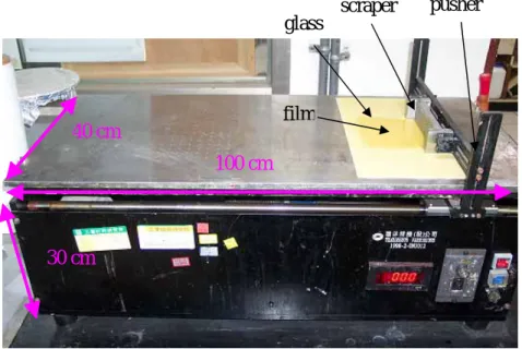
(14) Figure 3.3 Two 2P orbits form the πbond………………………………………………32. Figure 3.4 (a) Structure of the carbon nanotube in different rolling direction s [6], (b) rolling direction of a graphene sheet (cited from the “Carbon Nanotube Activity Guide”, MRSEC)…………………………………………………………………………………33. Figure 3.5 Chiral vector OA is expressed as Ch=na1+ma2, (n,m)=(4,2)…………………34 Figure 3.6 The structure of a multiwall carbon nanotube……………………………….36. Figure 3.7 The separation between two adjacent layers of a MWCNT is around 0.34 nm………………………………………………………………………………………..36. Figure 3.8 Molecular distribution after solidification of (a) LCP and (b) semi-crystalline plastic…….………………………………………………………………………………38. Figure 3.9 Chemical expression of an imide monomer………………………………….39. Figure 3.10 Schematic drawing of a CVD instrument…………………………………...41. Figure 3.11 Carbon nanotube growth mechanisms of CVD method (a) tip-growth and (b) base-growth………………………………………………………...…………………….42. Figure 3.12 Schematic drawing for arc-discharge deposit method………………………43. Figure 3.13 (a) The SEM photo of CNTs (b) the TEM photo of CNT…………………..45. Figure 3.14 Schematic drawing of laser ablation method………………………………..46. Figure 3.15 Photo of a thermal compression molding machine…………………………47. vi.
(15) Figure 3.16 Photo of the machine for scraping the MWCNT-PAA thin film…………...48. Figure 4.1 SEM photos of (a) MWCNTs embedded in LCPs and (b) MWCNTs distribution in composite…………………………………………………………………52. Figure 4.2 Energy states of metal, semiconductor, and graphite………………………..53. Figure 4.3 Schematic of four-point-probe method……………………………………....54. Figure 4.4 Electrical conductivity as a function of mass fraction of MWCNT-LCP composite………………………………………………………………………………...56. Figure 4.5 (a) Measurement setup for the shielding effectiveness of the plastic composites based on the ASTM D4935 method, and (b) a cross section of the coaxial-type transmission-line holder………………………………………………………………….58 Figure 4.6 Equivalent circuit of the SE measurement by the flanged coaxial transmission line………………………………………………………………………………………..58. Figure 4.7 (a) Far-field measurement of 50 wt% MWCNT-LCP composite. (b) Relations of SE and frequency for different weight percentages of CNTs filled CNT-LCP composites………………………………………………………………………………..62. Figure 4.8 (a) MWCNT-LCP package, (b) monopole type antenna, (c) optical transmitter, (d) optical receiver……………………………………………………………………….63. Figure 4.9 An SE measurement setup for near-field monopole-type source in a fully anechoic EMC chamber………………………………………………………………….64. Figure 4.10 Limits for radiated emission of Class A and Class B in both FCC and CISPR 22 standard in a distance of 10 meters…………………………………………………...66. vii.
(16) Figure 4.11 (a) Near-field shielding effectiveness results and (b) received radiations of monotype antenna enclosed in a 50% weight percentage MWCNT-LCP box………….69. Figure 4.12 (a) Near-field shielding effectiveness results and (b) received radiations of 2.5Gbps optical transmitter………………………………………………………………71. Figure 4.13 (a) Near-field shielding effectiveness results and (b) received radiations of 2.5Gbps optical receiver…………………………………………………………………73. Figure 4.14 The EMS measurement setup……………………………………………….76. Figure 4.15 Eye diagrams of the packaged module in (a) 20 wt% (b) 30 wt% (c) 50 wt% MWCNT-LCP composites under radiation interference. The arrows indicate the worse jitters surrounding at X region…………………………………………………………...77. Figure 4.16 The relationship between mask margin and MWCNT weight percentage at the amplitude of monopole type antenna of 0.75 Vpp…………….…………………….78. Figure 4.17 The BER versus the received optical power for three different cases, unpackaged module without radiated interference (case A), unpackaged module with radiated interference (case B), and packaged module with radiated interference (case C)…………………………………………………………………………………………79. Figure 4.18 The relationship between power penalty and CNT weight percentage at the amplitude of monopole type antenna of 1Vp-p………………………………………….80. Figure 5.1 The chemical expression of HDMIC ionic liquid dispersant………………...87. Figure 5.2 (a) Schematic diagram of aggregated MWCNTs, (b) ionic liquid (IL), and (c) aggregated MWCNTs with IL in NMP solvent………………………………………….88. viii.
(17) Figure 5.3 (a) Schematic diagram of MWCNTs dispersed by IL, (b) well-dispersion MWCNTs by IL………………………………………………………………………….89 Figure 5.4 Raman spectroscopy shows peaks of IL dispersed MWCNT-PI at 1580 cm-1 and 1350 cm-1, which are essentially identical to the non-dispersed MWCNT-PI………92. Figure 5.5 UV-vis spectrometer absorption of various weight ratios of MWCNT-IL hybrid dispersed in NMP solvent at wavelength of 550 nm……………………………..93. Figure 5.6 The relationship between electrical conductivity of MWCNT-PI composite and MWCNT weight percentage in the composite, it indicates the lower percolation thresholds of IL (HDMIC) dispersed than without IL dispersed………………………...95. Figure 6.1 (a) MWCNTs (ADM), (b) MWCNTs (CVD)………………………………100. Figure 6.2 UV-vis spectrometer absorption of various weight ratios of MWCNT-IL hybrid dispersed in NMP solvent at wavelength of 550 nm……………………………102. Figure 6.3. SEM photo of MWCNT-PI composite……………………………………..102. Figure 6.4 SEM photos of the IL dispersed 30 wt% MWCNT-PI composite. (a) magnification x1000 (b) magnification x 2000 (c) magnification x 5000 (d) magnification x 10000………………………………………………………………………………….103 Figure 6.5 Relation between MWCNT weight percentage and electrical conductivity of (a) IL dispersed MWCNT-PI composite and (b) MWCNT-LCP composite………………104. Figure 6.6 SE of dispersed 30 wt% MWCNT-PI, 50 wt% and 30 wt% MWCNTLCP……………………………………………………………………………………..105. Figure 6.7 The MWCNT-PI package…………………………………………………...106. ix.
(18) Figure 6.8 (a) Received radiations and (b) Near-field SE of monotype antenna enclosed in a 30 wt% MWCNT-PI box…………………………………………………………….107. Figure 6.9 Setup for receiver performance measurement………………………………108. Figure 6.10 Eye-diagrams of 2.5 Gbps optical receiver (a) without shield and (b) with shield……………………………………………………………………………………109. Figure 6.11 Mask margins of with shield and without shield optical receiver under different interference voltage amplitudes of a monopole type antenna………………...110. Figure 6.12 Mask margins of with shield and without shield optical transmitter under different interference voltage amplitudes of a monopole type antenna………………...111. Figure 6.13 The BER versus the received optical power for three different cases. Case A (unpackaged module with radiated interference), Case B (packaged module with radiated interference), and Case C (unpackaged module without radiated interference)……….112. x.
(19) LIST OF TABLES Table 3.1 Comparison between CNT and other materials……………………………….30. Table 3.2 Process characteristic comparison of CVD, ADM, and laser ablation……...40. Table 3.3 The advantage and disadvantage comparison of CVD, ADM, and laser ablation…………………………………………………………………………………..41. Table 4.1 Limits for radiated emission of FCC Class B devices………………………...66 Table 5.1 Binding energies of van der Waals force, cation- π interaction, alkyl-alkyl interaction, and alkyl-polyimide interaction……………………………………………..91. xi.
(20) CHAPTER 1 INTRODUCTION 1.1 Background The trend of high-speed electronics is low voltage and low power, the electromagnetic interference (EMI) and electromagnetic susceptibility (EMS) or electromagnetic (EM) immunity of the optical transceiver modules to the EMI become the major concerns to constrain the unintended EM emissions from the electronic apparatus within the regulation limitation, and meanwhile to maintain a good signal quality of over gigabit transmission rate [1-3]. The design of electronic apparatuses takes EMI and EMS into account is called the electromagnetic compatibility (EMC) design. Basically, a well EMC designed electronic apparatus is able to minimize the unintended interference. The unintended interference mainly comes from radiation emission and conduction emission [4]. Although a lot of EMC designing hints are mentioned and described in some relevant textbooks and literatures [4-5], to completely eliminate the EMI at the circuit design level is still very difficult at all. For reducing the influence of the radiation emission, a package with EM shielding capability is usually adopted, which is a more practical and essential approach, especially while applied in the real commercial products. In this study, the fabrication of the novel EM shielding materials, the shielding effectiveness (SE) of these novel EM shielding materials, and their packaging applications are the main subjects of this thesis. As for the elimination of conduction emission, that is mainly from the accessory parts such as signal cables and power wires, which is not the study focus in this thesis. However, for reducing the influence of conduction emission, the cable shield and ground must have an overall consideration in system level. In most applications the electronic apparatuses are not isolated, the power wires, ground wires, and signal cables used to connect with external plugs, sockets, and other instruments, are necessary. So the conduction emission is possible to enter or exit the apparatus via these conductive paths. While designing a system, this kind of interference must be treated well, and usually an optimized grounding design is the key to overcome the interference from conduction emission.. 1.
(21) To improve the EMI and EMS performance of the high-speed transmission electronic apparatuses, the high EM shielding packaging or housing is desirable, such as the packaging of the optical transmitter and receiver modules in this study. The optical transceiver module comprises the optical transmitter and optical receiver is commonly used for optical fiber communication, and widely applied from the intercontinental longhaul undersea optical fiber communication, the metropolitan networking, to the so-called last-mile fiber to the home (FTTH) optical fiber communication. Besides, some high performance computers and specific processors need the optical fiber transmission to expedite the data transmission flow. Conventionally, metals are the major materials for packaging, the metal armored package can offer strong mechanic protection for the inside electronic parts, and also can provide the best SE. There are some popular packaging designs for optical transceivers in various applications, such as Butterfly, DIL (dual-inline), and TO-can (transistor outline). Each design has its application preference. In practice, the Butterfly package is usually used for high transmission speed (10 Gbps and above) and applied in long-haul optical fiber communication. It is because of the short wire connections between the chip pads and the lead pins are essential to prevent the signal loss and signal reflection in the electrical paths, especially while operating in a high transmission speed. TO-can package is usually used in the short distant data transmission, and the speed is relative lower, such as 155 Mbps. TO-can itself is a metallic package, however the final package for 155 Mbps optical transceiver module with TO-cans is usually plastic but with metal foils underneath due to the low cost and light weight concern. Recently, there is high speed TO-can design released for 10 Gbps after overcoming the cooling and process issue [3].. 1.2 Motivation. It is well known that metallic package can provide an excellent SE. However, the characteristics of low cost and easy manufacturing have promoted the plastic composite package as the most suitable material for fabricating the optical transceiver modules applied in the fiber to the home (FTTH) applications [3,6-9].. 2.
(22) Plastics alone are inherently transparent to the EM radiation and provide no shielding against the radiation emissions. To give EM shielding capability for the plastic packaging, electrical conductive properties must be added into the plastic hosts for the adequate EM shielding. The currently available techniques for providing EMI shielding include electro-plating, electroless-plating, conductive sprays, zinc-arc spraying, conductive painting, conductive fillers, and other metallization processes. Among these methods, the most potential one for EM shielding is to compound plastics with discontinuous electronic conductive fillers such as metal particles, metal flakes, stainless fiber, graphitized carbon particles, graphitized carbon fibers, metal-coated glass, and carbon fibers [9-11]. Recently, several types of plastic composite package for the optical transceiver modules have been demonstrated with effective EM shielding ability. These plastic composites are the nylon and liquid crystal polymer (LCP) reinforced with carbon fibers [12-13], the woven continuation fiber (WCCF) [3,9,14]. Due to the fact of the remarkable electrical and mechanical properties of the carbon nanotubes (CNTs) [15-16], the CNTs have been the focus of considerable researches and developments for use in nanoscale electronic and optoelectronic applications such as integrated circuit (IC) interconnections [17], and optical emission devices [18].. 1.3 Objective. In this study, the multiwall carbon nanotubes (MWCNTs) are considered as the electrical conductive fillers because of their known properties of high electrical conductivity, nanoscale diameter, high aspect ratio, and possibly strengthened mechanical properties [15-16]. The aspect ratio of the MWCNTs is around 200 ~ 500 in this study, some reported lab-made and commercial products even higher than 1000, which offers the intensive interconnection in the MWCNT-plastic networking and results in a high EM shielding ability.. 3.
(23) Figure 1.1 FCC regulation for the received radiative electrical field limit of Class A and Class B [4]. To comply with the Federal Communications Commission (FCC) EMI regulation (refer to Figure 1.1), maintaining both high EMI shielding and EMS performance of the electronic apparatuses are required. In this study, the novel liquid crystal polymer (LCP) based MWCNT composites with high SE and effective EMS performance used in packaging a 2.5 Gbps plastic transmitter and receiver modules are proposed. The results demonstrated that the plastic transmitter and receiver modules with more weight percentages of the MWCNTs exhibit higher SE, and hence show excellent EMS performance, a better mask margin, and a lower power penalty. This indicates that the polymer-based MWCNT composites with their high SE are suitable for packaging low cost and high performance EMS optical transceiver modules used in FTTH lightwave transmission systems [19-20]. However, the high aspect ratio and low ionic character make MWCNTs not easily dispersed within the plastic hosts. The lack of dispersing ability in the polymer matrices is caused by internal van der Waals force among the MWCNTs and their consequent aggregation [21-26]. Without a fine dispersion, the MWCNTs may form local clusters and poor homogeneity in the MWCNT plastic composites. As a consequence, the adequate weight percentage of the added MWCNTs is required to achieve a good electrical conductivity and a comparable SE. For developing a cost effective material, a fine dispersion of MWCNTs in the polymer matrices is essential.. 4.
(24) The physical mechanism of MWCNTs dispersion is investigated and modeled in this study. To understand the dispersion mechanism is useful for the process improvement and also for cost saving. The MWCNTs need purification and dispersion before application. Otherwise they are impure and aggregated as clusters in the host matrices. The aggregation phenomenon of MWCNTs is negative for making a homogeneous mixture due to the predominant electrical conductive MWCNTs networking is difficult to be constructed inside the host matrices. The MWCNT as guest material, its content has to be increased in order to build the effective networking paths. However if the mixture is uniform and homogeneous then the percolation threshold can be achieved under a lower volume fraction. That means the effective networking can be built under lower guest concentration if the mixture is homogeneous and uniform. For the purpose of uniform dispersion, the ionic liquid (IL) dispersant is adopted. The complex intermolecular interaction forces induced by the addition of IL have to be taken into account. This is a complex micro system in the molecular scale. Some experimental measurements were done to help the understanding via comparing the macro parameters such as electrical conductivity, uniformity index, and SE. And some measurements were done in the micro or nano scale such as observing the metallographies by scanning electrical microscope (SEM) and transmission electrical microscope (TEM), and even measuring the absorption spectrum by the Raman spectrometer. In this study, we also presented the EM shielding performance of a plastic composite by employing polyimide (PI)-based dispersed MWCNTs. The MWCNT-PI films were prepared by using a physical dispersed method to disperse MWCNTs into PI resin. The MWCNT-PI composites were then formed by stacking several thin films. The resultant package of the composites with 30 wt% MWCNTs can exhibit high SE of 40 dB ~46 dB in the far field measurement within the frequency range from 1GHz to 3 GHz. In addition, the package housing fabricated by the dispersed MWCNT composites showed an enhanced EMS performance, an improved mask margin, and a lower power penalty for a 2.5 Gbps lightwave transmission system. The ionic liquid (IL) dispersed MWCNT composites are proven to be suitable for packaging low-cost and high-performance optical transceiver modules for use in the FTTH lightwave transmission systems.. 5.
(25) 1.4 Organization. This thesis comprises several chapters. The electromagnetic shielding theory described in chapter 2 includes the introduction of the shielding effectiveness under far field and near field. Chapter 3 mentioned about the shielding material fabrication, including the introduction of nanotube properties, properties of engineering plastic matrices - liquid crystal polymer and polyimide, the fabrication methods of carbon nanotubes, and the fabrication methods of carbon nanotube plastic composites. Chapter 4 demonstrated the EM shielding performance of the MWCNT-LCP composite and its application in packaging. Chapter 5 focused on the MWCNT dispersion, including the dispersion mechanism investigation. Chapter 6 demonstrated the shielding performance of the dispersed MWCNT-PI composite and its application in packaging. The summary of this study is finally concluded in chapter 7.. References. [1] J. T. DiBene, and J. L. Knighten, “Effects of device variations on the EMI potential of high speed digital integrated circuits”, IEEE Electromagn. Compat., pp. 208-212, Aug. 1997. [2] D. M. Hockanson, X. Ye, J. L. Drewniak, T. H. Hubing, T. P. V. Doren, and R. E. DuBroff, “FDTD and Experimental Investigation of EMI from Stacked-Card PCB Configurations”, IEEE Trans. Electromagn. Compat., vol. 43, no. 1, pp. 1-9, Feb. 2001. [3] T. L. Wu, M. C. Lin, C. W. Lin, T. T. Shih, and W. H. Cheng, “High electromagnetic susceptibility performance plastic package for 10 Gbit/s optical transceiver modules”, Electron. Lett., vol. 41, no. 8, pp. 494–495, Apr. 2005. [4] C. R. Paul, “Introduction to Electromagnetic Compatibility”, A Wiley-interscience Publication, 1992. [5]. H. W. Ott “Noise Reduction Techniques in Electronic Systems”, A Wileyinterscience Publication, 1988.. 6.
(26) [6]. K. Tatsuno, K. Yoshida, T. Kato, T. Hirataka, T. Miura, K. Fukuda, T. Ishikawa, M. Shimaoka, and T. Ishii, “High-performance and low cost plastic optical modules for access network system applications”, J. Lightwave Technol., vol. 17, no.7, pp. 1211–1216, Jul. 1999.. [7] M. Fukuda, F. Ichikawa, Y. Shuto, H. Sato, Y. Yamada, K. Kato, S.Tohno, H. Toba, T. Sugie, J. Yoshida, K. Suzuki, O. Suzuji, and S.Kondo, “Plastic module of laser diode and photodiode mounted on planar lightwave circuit for access network”, J. Lightwave Technol., vol.17, no. 7, pp. 1585–1590, Jul. 1999. [8]. T. L. Wu, W. S. Jou, S. G. Dai, and W. H. Cheng, “Effective electromagnetic shielding of plastic packaging in low-cost optical transceiver modules”, J. Lightwave Technol., vol. 21, no. 6, pp. 1536–1543, Jun. 2003.. [9]. W. H. Cheng, W. C. Hung, C. H. Lee, G. L. Hwang, W. S. Jou, and T. L. Wu, “Low cost and low electromagnetic interference packaging of optical transceiver modules”, J. Lightwave Technol., vol. 22, no. 9, pp. 2177–2183, Sept. 2004.. [10] P. B. Jana, A. K. Mallick, and K. De, “Effects of sample thickness and fiber aspect ratio on EMI shielding effectiveness of carbon fiber filled polychloroprene composites in the X-band frequency range”, IEEE Trans. Electromagn. Compat., vol. 34, no.11, pp. 478–492, Nov. 1992. [11] P. F. Wilson, M. T. Ma, and J.W. Adams, “Technique, for measuring the electromagnetic shielding effectiveness of materials. I. Far-field source simulation”, IEEE Trans. Electromagn. Compat., vol. 3, no. 8, pp. 239–247, Aug. 1988. [12] W. S. Jou, T. L. Wu, S. K. Chiu, and W. H. Cheng, “Electromagnetic shielding of nylon-66 composites applied to laser modules”, IEEE/TMS J. Electro. Material, vol. 30, no. 10, pp. 1287–1293, Oct. 2001. [13] W. S. Jou, T. L. Wu, S. K. Chiu, and W. H. Cheng, “The influence of fiber orientation on electromagnetic shielding in liquid crystal polymers”, IEEE/TMS J. Electro. Material, vol. 31, no. 3, pp. 178–184, Mar. 2002. [14] T. L. Wu, W. S. Jou, W. C. Hung, C. H. Lee, C.W. Lin, and W. H. Cheng, “High electromagnetic shielding of plastic package for 2.5 Gbps optical transceiver modules”, IEEE Trans. Adv. Packag., vol. 28, no. 1, pp. 89-95, Feb. 2005.. 7.
(27) [15] E. D. Minot, Y. Yaish, V. Sazonova, J. Y. Park, M. Brink, and P. L. McEuen, “Turning carbon nanotube band gaps with strain”, Phys. Rev. Lett., vol. 90, no. 15, pp. 154601–154604, Apr. 2003. [16] K. B. K. Teo, etc, “Carbon nanotube technology for solid state and vacuum electronics”, IEE Proc.-Circuits Devices Syst., vol. 151, no. 5,pp. 443-451, Oct. 2004. [17] J. Li, Q. Ye, A. Cassell, H. T. Ng, R. Stevens, J. Han, and M. Meyyappan, “Bottomup approach for carbon nanotube interconnects”, Appl. Phys. Lett., vol. 82, no. 15, pp. 2491–2493, Apr. 2003. [18] J. A. Misewich, R. Martel, P. Avouris, J. C. Tsang, S. Heinze, and J. Tersoff, “Electrically induced optical emission from a carbon nanotube FET”, Science, vol. 300, pp. 783–786, May 2003. [19] C. M. Chang, J. C. Chiu, W. S. Jou, T. L. Wu, and W. H. Cheng, “New package scheme of a 2.5Gb/s plastic transceiver module employing multiwall nanotubes for low electromagnetic interference”, IEEE J. Sel. Topics Quantum Electron., vol. 12, no. 5, pp. 1025-1031, Sept/Oct. 2006. [20] C. M. Chang, M. C. Lin, J. C. Chiu, W. S. Jou, and W. H. Cheng, “Highperformance electromagnetic susceptibility of plastic transceiver modules using carbon nanotubes”, IEEE J. Sel. Topics Quantum Electron., vol. 12, no. 6, pp. 10911096, Nov/Dec. 2006. [21] M. F. Islam, E. Rojas, D. M. Bergey, A. T. Johnson, and A. G. Yodh,”High Weight Fraction Surfactant Solubilization of Single-Wall Carbon Nanotubes in Water”, Nano Lett., 3, pp. 269–273, 2003. [22] V. C. Moore, M. S. Strano, E. H. Haroz, R. H. Hauge, R. E. Smalley, J. Schmidt, and Y. Talmon, ”Individually Suspended Single-Walled Carbon Nanotubes in Various Surfactants”, Nano Lett., 3, pp. 1379–1382, 2003. [23] O. Matarredona, H. Rhoads, Z. Li, J. H. Harwell, L. Balzano, and D. E. Resasco, ”Dispersion of Single-Walled Carbon Nanotubes in Aqueous Solutions of the Anionic Surfactant NaDDBS”, J. Phys. Chem. B, 107, pp. 13357–13367, 2003. [24] V. A. Sinani, M. K. Gheith, A. A. Yaroslavov, A. A. Rakhnyanskaya, K. Sun, A. A. Mamedov, J. P. Wicksted, N. A. Kotov, “Aqueous dispersions of single-wall and. 8.
(28) multiwall carbon nanotubes with designed amphiphilic polycations”, Journal of the American Chemical Society, 127, pp. 3463-3472, 2005. [25] Y. Kang and T. A. Taton, “Micelle-Encapsulated Carbon Nanotubes: A Route to Nanotube Composites”, J. Am. Chem. Soc., 125, pp. 5650 – 5651, 2003. [26] C. Y. Li, L. Li, W. Cai, S. L. Kodjie and K. K. Tenneti, “Nano-Hybrid Shish-kebab: Polymer decorated carbon Nanotubes”, Adv. Mater. 17, pp.1198-1202, 2005.. 9.
(29) CHAPTER 2 ELECTROMAGNETIC SHIELDING THEORY Electronic circuits need packaging to get an adequate mechanical protection to avoid the possible damage during manipulation and assembly, such as the soldering and mounting upon the system module boards. Packaging is necessary especially when delivering the final commercial products, such as televisions, radios, and computers, to the end users. Usually, the electronic products need adequate metal packaging to enclose the whole electronic circuits. The first reason is due to the metal can offer an excellent mechanic protection to avoid the risky damage from external forces such as collision and pressure. The second reason is to protect the enclosed electronic circuits from being damaged by a direct electrical static discharge (ESD), where the metallic package can offer a discharge path outside the enclosed electronic circuits. The third reason is to protect the end users from being hurt by the electrical shocks. And the last and most important reason is to offer an excellent electromagnetic shielding capability for the EMC concern. For EMC concern, the packaging of the electronic devices is requested to maintain an adequate electromagnetic shielding capability to avoid the unintended electromagnetic radiation from the enclosed electronic circuits leaking to the ambient environment. Because these unintended radiations could influence the ambient electrical facilities, such as wireless communication and radio broadcasting, even possibly injury human health. It is the so-called EMI concern. In fact, there are a few governmental organizations responsible to define the rules and constraints for EMI such as the famous FFC regulations in USA and the FTZ/VDE in Germany. The packages are also used to protect the enclosed electronic circuits from the external interference emission, that means to reduce the influence from the neighboring external radiation sources such as the strong radiations from the radio stations, mobile base stations, and TV stations. It is the socalled electromagnetic susceptibility (EMS) concern. For this, the packaged electronic devices are tested to understand their EMS performance. In general, the interference emission sources are from two major parts, one is the radiated emission (30 MHz~12 GHz) and another is the conducted emission (several. 10.
(30) KHz~30 MHz) [1]. The radiated emission is in the form of electromagnetic wave, which transmits the electric and magnetic fields in the air, such as the intended radiation electromagnetic wave from the radio broadcasting antenna and the unintended radiation electromagnetic wave from the high-speed transceivers. As for the conducted emission, it is the noise from the poor EMC designed inter-connections such as electrical cables and power wires. And the noise is possible to influence the electronic circuits seriously. While mentioning about the electromagnetic shielding, it is usually relevant to the radiated emission only. The conducted emission is another subject especially for the noise prevention in system level. Figure 2.1 shows the frequency spectrum, which covers from the AM radio band (~106 Hz) to the Gamma ray band (~1018 Hz) [2]. The so-called radio frequency (RF) focuses on the range from 3 Hz to 300 GHz [3]. And as for the microwave frequency, it is part of the RF range, and it focuses in the frequency range from 30 MHz to 300 GHz [4].. Figure 2.1 Frequency spectrum from AM radio to Gamma rays [2].. 2.1 Mathematical Model of Shielding Effectiveness. The electromagnetic shielding capability of a material is called shielding effectiveness (SE). Fundamentally it is the insertion loss of the shielding material, and it is defined as the ratio of incident power to the transmitted power. Usually the ratio is expressed in decibel unit as. 11.
(31) SE = 10 log10. Pi Pt. (2-1). where Pi is the incident power to the material, and Pt is the transmitted power which penetrates through the material. Figure 2.2 illustrates the EM wave reflection and transmission upon a material. A normal uniform planar wave is incident to the material from the left side. The material is with the thickness of t, and with the electrical conductivity of σ, the permittivity of ε, and the permeability of µ.. t Ei. Et. Hi. σ,µ,ε. Ht. Er Hr. Figure 2.2 A uniform plane wave is normal incident to a material.. The uniform electromagnetic planar wave with the electric field Ei and the magnetic field Hi is incident into the material from the left side. Part of the incident electromagnetic wave is reflected in the opposite direction with field Er and field Hr. However, still part of the incident wave is transmitted through the material to the right side with fields Et and Ht. The electric field shielding effectiveness of the material can be expressed as. 12.
(32) SE = 20 log10. Ei Et. (2-2). And the magnetic field shielding effectiveness of the material can be expressed as. SE = 20 log10. Hi Ht. (2-3). If the media in the left of the material is identical with the right, then the equations (2-2) and (2-3) are exactly equal. Because the intrinsic impedance of the media is the ratio of the electric field to the magnetic field. If the media is the air then the impedance of E/H is a constant of 377 Ω.. Figure 2.3 Reflection and transmission of an incident wave to a material.. Theoretically the shielding effectiveness of a material is contributed from three main portions. They are the reflection loss, the absorption loss, and the multi-reflection loss. As shown in Figure 2.3, the incident wave from left of the material is reflected partially, and the other portion continuously penetrates into the material. Then the penetrated wave will be transmitted inside the material and attenuated due to the absorption of the material. Once the remaining transmitted wave arrived at the right interface, the second reflection. 13.
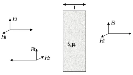
(33) is occurred and the second reflected wave will transmit in the opposite direction, toward left. And the rest wave continuously penetrates the right interface, then exit to the right media. The second reflected wave transmitted toward left is attenuated until arriving the left interface. Then the penetration and reflection will occur again, this kind of phenomenon will repeatedly happen again and again. So the incident wave is declined by the reflection and the absorption. In case the material thickness is much greater than the skin depth then the multi reflection can be ignored. Because the attenuation increases as the transmission distance increases, the wave is attenuated to 1/e at skin depth, if the material thickness is longer than skin depth then there is just few succeeding reflection can be sustained. So the total shielding effectiveness can be expressed as. SE dB = RdB + AdB + M dB. (2-4). where RdB is the reflection loss, AdB is the absorption loss, and MdB is the multi-reflection loss. The electromagnetic shielding effectiveness of the material depends on the distance between radiation source and the shielding material. While the radiation source is quite far from the shielding material, the shielding effectiveness is called as far field SE, it will be described in section 2.2. As for the short distance case, it is called as near field SE and will be described in section 2.3.. 2.2 Shielding Effectiveness in Far Field. When the incident radiation source of the material is very far from the shielding material (greater than λ. 2π. ), then the incident field of the material can be considered as a. uniform planar wave. That radiation source is called as far field source. Here we consider. 14.
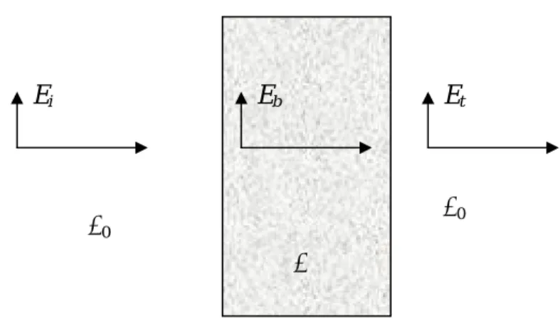
(34) the approximate solution that assumes the thickness of material is much greater than the skin depth under the operation frequency.. Ei. Eb. Et. η0. η0 η. Figure 2.4 The electric field Ei from air is incident into a material with the characteristic impedance η, Eb is the electric field that transmits inside the material, and Et is the electric field that transmits through the material.. As shown in Figure 2.4, the incident uniform planar wave with electric field Ei is incident into the material from the air in left side. Partial wave transmits into the material with the electric field Eb, so the coefficient of transmission in the left interface is Eb/Ei. Then the wave with field Eb will continuously goes through the right material interface and transmits to the air as field Et, so the coefficient of transmission in the right interface is denoted as Et/Eb. Here the shielding effectiveness of the material from reflection can be expressed as Et/Ei, which can be further calculated as [5]. 2η 0 4η0 η Et E E 2η = t b = = Ei Eb Ei η 0 + η η0 + η (η0 + η)2. (2-5). 15.
(35) where η0 is the wave impedance of air, and η is the characteristic impedance of the shield material.. In case the material is a good conductor, then η << η 0. Substitute formula (2-5) into formula (2-2), then [5]. RdB = 20 log10. where. η=. (η0 + η)2 Ei η = 20 log10 ≅ 20 log10 0 Et 4η 0 η 4η jϖµ ≅ σ + jϖε. jϖµ σ. , η0 =. (2-6). µ0 ε0. So RdB can be expressed as [5]. ⎛1 σ RdB = 20 log10 ⎜⎜ ⎝ 4 ϖµ r ε 0. ⎞ ⎟ ⎟ ⎠. (2-7). where µ r is the relative permeability ( µ = µ 0 µ r ), µ 0 is the permeability of air, ε 0 is the permittivity of air, σ is the electrical conductivity, then RdB can be further expressed as [5-6] ⎛ σ RdB = 168 + 10 log10 ⎜⎜ r ⎝ µr f. ⎞ ⎟⎟ ⎠. (2-8). where ϖ = 2πf , σ r = σ / σ Cu is the relative conductivity of the material, it is related to the electrical conductivity of the copper , the electrical conductivity of copper is σ Cu = 5.8 × 10 7 S. m. .. 16.
(36) So far the attenuation of the electromagnetic wave in the material during wave propagation is not taken into account, the Eb amplitude is assumed not attenuated inside the material.. However, the attenuation is really happened inside the shielding material due to the absorption loss, the amplitude of the EM wave is declined during wave traveling, and it can be mathematically expressed as [5-6]. AdB = 131.4t fµ r σ r. (2-9). As for multi-reflection loss, it can be mathematically expressed as [5-6]. 2. M dB. ⎛ η − η ⎞ − 2 t / δ − j 2 βt ⎟⎟ e = 20 log10 1 − ⎜⎜ 0 e ⎝η0 + η ⎠. (2-10). ≅ 20 log10 1 − e −2t / δ e − j 2t / δ where t is the thickness of the shielding material, and δ is the skip depth under the operation frequency, β is the propagation constant.. It can be ignored if the thickness of the shielding material is greater than the skin depth under the operation frequency and a good conductor. The transmitted EM fields will be dramatically attenuated during a long-distance propagation inside the shielding material. But when the shielding material is not thick enough, and thinner than then skin depth, then the multi-reflection loss will be negative.. 17.
(37) The multi-reflection phenomenon is especially easy to happen for the magnetic field, since most incident magnetic fields are penetrated through the entry interface of the shielding material and most penetrated magnetic fields are reflected from the exit interface of the shielding material. But as for the electrical field, the multi-reflection is usually not a serious problem because most of the incident electrical fields are reflected from the entry interface of the shielding material, and just few penetrated electrical fields reflected from the exit interface. There are not many electrical fields left for multireflection in the shielding material, especially when the shielding material is a good electrical conductive material. The less multi-reflection phenomenon of the electrical fields can be understood from the formula Eb = 2η Ei / (η0 + η), where the shield is assumed as a good electrical conductive material, so the electrical conductivity of the material η is with a low impedance and less than η 0 . So basically the electrical field Eb that penetrated through the entry interface is small, there is only few electrical field can be retained for multi-reflection. As for the magnetic field, the behavior is reversed. Because according to the formula Hb = 2η0 Hi / (η0 + η), the penetrated magnetic fields H b are remarkable. So the multireflection is a real problem for magnetic field. The influence is more important in the low frequency (such as several KHz) for the magnetic field dominant radiation since the overall shielding effectiveness is low. However, once the frequency gets higher (such as several GHz), the negative contribution from the multi-reflection can be reduced. That’s due to the ratio between material thickness and skin depth became larger as the frequency increases.. In summary, the total far field SE is the summation of the equations (2-8), (2-9), and (2-10). Figure 2.5 plots the numeric calculations for each contribution factor and their sum. This example assumed a material under far field measurement is with thickness of 0.85 mm, electrical conductivity of 6 S/cm, and frequency range within 1 GHz ~ 3 GHz. In Figure 2.5, the reflection loss decreases as the frequency increases, the absorption loss increases as the frequency increases, and the multi-reflection loss slightly decreases as the frequency increases. However, the multi-reflection term is very small, it is about 18.
(38) 0.517 dB ~ 0.016 dB. That is due to the skin depth is smaller than the material thickness of 0.85 mm, the skin depth is about 0.649 mm ~ 0.375 mm within the frequency range of 1 GHz ~ 3 GHz.. 60. Reflection Aborption Multi-reflection Total SE. 50. SE (dB). 40 30 20 10 0 1. 1.5. 2. 2.5. 3. GHz. Figure 2.5 Numeric calculation results for reflection loss, absorption loss, multireflection loss, and the total shielding effectiveness under far field condition.. 2.3 Shielding Effectiveness in Near Field. When the distance between the radiation source and the shielding material is less than λ. 2π. , it is the near field. The uniform planar wave assumption used in the far field. cannot sustain in the near field. Because the wave front in the near field is not planar but curved, so the wave front is not parallel to the surface of the shielding material. The wave 19.
(39) impedance of the near field is not like that of the far field. The wave impedance is a constant in the far field, but the wave impedance of the near field varies with the distance between radiation source and the shielding material. It is not like the constant wave impedance of η 0 =. µ0 = 377Ω in the far field. ε0. The wave impedance. E of the near field depends on the distance and the dominant H. field. In case it’s an electrical radiation source, that means the electrical field dominates the magnetic field, then it will demonstrate high wave impedance. But the wave impedance decreases as the distance increases in the near field, it can be express as [6]. η0 =. 1 2πfεr. (2-11). Then we substitute equation (2-11) into equation (2-6) to result in the following expression of equation (2-12) [5-6]. It is the near field shielding effectiveness of the reflection loss contribution under the electrical field dominated condition.. ⎛ σr ⎞ ⎟ Re ,dB = 322 + 10 log10 ⎜⎜ 3 2 ⎟ f r µ ⎝ r ⎠. (2-12). In case it’s a magnetic radiation source, then the wave impedance will be lower than 377 Ω . And the wave impedance increases as the distance increases, it can be expressed as [6]. η 0 = 2πfµr. (2-13). Substituting equation (2-13) into equation (2-6) to result in expression (2-14) [5-6].. 20.
(40) Rm ,dB. ⎛ fr 2 σ r = 14.57 + 10 log10 ⎜⎜ ⎝ µr. ⎞ ⎟ ⎟ ⎠. (2-14). As for the absorption loss contribution to the total shielding effectiveness in the near field, it is as same as equation (2-9). Both the electrical field and magnetic field, the absorption loss term is same.. 2.4 Shielding Effectiveness Model for Mixing Materials. A composite comprises the guest materials and the host material. In this study the guest material is the electrical conductive MWCNT, and the host material is the insulated engineering plastic such as LCP and PI. The electromagnetic shielding effectiveness of the plastic composite can be measured experimentally, and it also can be theoretically calculated according to the ratio of the incident electromagnetic wave to the transmitted electromagnetic wave that passes through the composite. Within the calculation there is an important parameter, the effective relative permittivity ε eff of the mixture composite, has to be known. The effective relative permittivity ε eff of the mixture composite can be approximately calculated from the mixing formula, such as the Maxwell Garnett formula. To characterize the electromagnetic properties of the composite, the electromagnetic parameters of guests and host must be known firstly. And the electromagnetic mixing formula is used to homogenize the mixture via an approximation approach to get the effective macroscopic parameters, such as the effective relative permittivity.. Using Maxwell Garnett mixing formula to calculate the effective relative permittivity of the mixture composite as expressed [7]. ε eff = ε e + 3 fε e. εi − εe ε i + 2ε e − f (ε i − ε e ). (2-15). 21.
(41) where ε e is the relative permittivity of host material (environment), ε i is the relative permittivity of spherical guest material (inclusion), f is the volume fraction of the inclusion within the mixture. The mixture of guest material and host material is shown in Figure 2.6.. εi. εe. Figure 2.6 Spherical particles with permittivity ε i spread inside the host material ε e .. As for the ellipsoidal inclusions, the Maxwell Garnett prediction can be adjusted and expressed as [7]. ε eff = ε e + ε e. f 3 1−. εi − εe j = x , y ,z ε e + N j (ε i − ε e ) N j (ε i − ε e ) f. ∑. 3. ∑. j = x , y ,z. (2-16). ε e + N j (ε i − ε e ). where N j is the depolarization factor of the ellipsoids that randomly oriented in the mixture.. 22.
(42) If the inclusions are electrical conductive (metallic) particles, their frequency characteristic in terms of relative permittivity is [7-8]. ε i (ω ) = ε ′ − jε ′′ = ε ′ − j. σ ωε 0. (2-17). where ε′ and ε′′ are the real part and the imaginary part of the complex relative permittivity of inclusion, σ is the electrical conductivity of the inclusion.. So far the effective relative permittivity of the mixture composite can be calculated approximately by the Maxwell Garnett formula. Then we can use this parameter to apply in the transmission coefficient calculation. And the over transmission coefficient of the composite can be converted to the shielding effectiveness easily via the logarithm process, since the decibel unit is the general expression for the SE.. Composite Air. Air. E incidence E transmission E reflection. Z0. Z0. Zm. z=l. z=0. Figure 2.7 Reflection and transmission of the EM wave between the air and the composite boundaries.. 23.
(43) Figure 2.7 shows the reflection and transmission of the EM wave in a composite material. The overall transmission coefficient can be expressed as [8]. T=. T1T2 e − γ ml 1 + R1 R2 e − 2 γ ml. (2-18). where T1 ,T2 are the transmission coefficients at the boundary z = 0 and at the boundary z = l , respectively. R1 and R2 stand for the reflection coefficients at the boundary z = 0. and at the boundary z = l , respectively. γ m is the complex propagation constant in the layer thickness of l . The R1 , R2 ,T1 ,T2 are further shown in the following expressions [8].. R1 =. Zm − Z0 Z −Z m , R2 = 0 Zm + Z0 Z0 + Zm. T1 =. 2Z m 2Z 0 , T2 = Z0 + Zm Zm + Z0. (2-19). and (2-20). where Z m , Z 0 are the characteristic impedance of the mixture composite and the air, respectively. They are expressed as [8]. Z0 =. µ0 µr , Zm = Z0 ε eff ε0. (2-21). And the propagation constant can be expressed as [8]. ′ γ m = jω µ 0 ε 0 ε ′eff − jε ′eff. (2-22). 24.
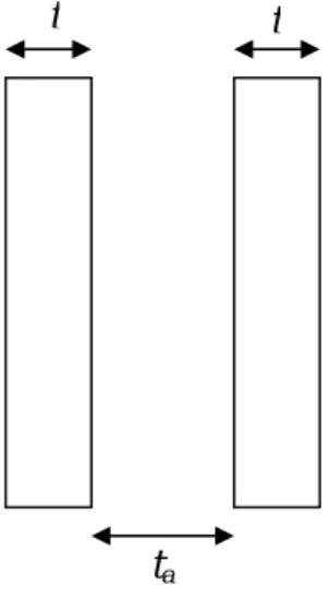
(44) So the shield effectiveness can be calculated as [8] SE = −20 log 10 ( T. ). (2-23). Substitute equations (2-19), (2-20), (2-21), and (2-22) into (2-18) to get overall transmission coefficient T. Then the SE of the composite can be calculated by converting the T into dB expression from equation (2-23).. 2.5 Shielding Effectiveness of Stacked Films. For increasing the shielding effectiveness, several electrical conductive thin films can be stacked layer by layer. Then the shielding effectiveness difference between the stacked thin films and a thick film (with the same thickness of stacked thin films) is discussed [910]. Firstly, to consider the simplest case, which two thin films with thickness t stacked together, but between these two thin films there is a ta air gap as shown in Figure 2.8.. t. t. ta Figure 2.8 An air gap of ta between two thin films with thickness t.. In Figure 2.8, the reflection loss, absorption loss, and multi-reflection loss can be expressed as [10]. 25.
數據
![Figure 1.1 FCC regulation for the received radiative electrical field limit of Class A and Class B [4]](https://thumb-ap.123doks.com/thumbv2/9libinfo/8894642.256457/23.892.210.697.168.428/figure-regulation-received-radiative-electrical-field-class-class.webp)
![Figure 2.1 Frequency spectrum from AM radio to Gamma rays [2].](https://thumb-ap.123doks.com/thumbv2/9libinfo/8894642.256457/30.892.199.717.558.768/figure-frequency-spectrum-radio-gamma-rays.webp)
+7

![Figure 3.7 The separation between two adjacent layers of a MWCNT is around 0.34 nm [8]](https://thumb-ap.123doks.com/thumbv2/9libinfo/8894642.256457/55.892.300.561.733.1018/figure-separation-adjacent-layers-mwcnt-nm.webp)

相關文件
volume suppressed mass: (TeV) 2 /M P ∼ 10 −4 eV → mm range can be experimentally tested for any number of extra dimensions - Light U(1) gauge bosons: no derivative couplings. =>
For pedagogical purposes, let us start consideration from a simple one-dimensional (1D) system, where electrons are confined to a chain parallel to the x axis. As it is well known
The observed small neutrino masses strongly suggest the presence of super heavy Majorana neutrinos N. Out-of-thermal equilibrium processes may be easily realized around the
Define instead the imaginary.. potential, magnetic field, lattice…) Dirac-BdG Hamiltonian:. with small, and matrix
incapable to extract any quantities from QCD, nor to tackle the most interesting physics, namely, the spontaneously chiral symmetry breaking and the color confinement..
(1) Determine a hypersurface on which matching condition is given.. (2) Determine a
• Formation of massive primordial stars as origin of objects in the early universe. • Supernova explosions might be visible to the most
The difference resulted from the co- existence of two kinds of words in Buddhist scriptures a foreign words in which di- syllabic words are dominant, and most of them are the
