國
立
交
通
大
學
電子工程學系電子研究所
碩 士 論 文
銅鎳奈米複合材料電遷移現象之研究
The Electromigration Study of Cu-Ni
Nanocomposite Stripes
研 究 生:朱家瑋
指導教授:鄭裕庭 教授
銅鎳奈米複合材料電遷移現象之研究
The Electromigration Study of Cu-Ni Nanocomposite Stripes
研 究 生:朱家瑋 Student:Cha-Wei Chu 指導教授:鄭裕庭 Advisor:Yu-Ting Cheng
國 立 交 通 大 學
電子工程學系電子研究所
碩 士 論 文
A ThesisSubmitted to Department of Electronics Engineering & Institute of Electronics College of Electrical Engineering and Computer Engineering
National Chiao Tung University in partial Fulfillment of the Requirements
for the Degree of Master
in
Electronics Engineering January 2011
Hsinchu, Taiwan, Republic of China
i
銅鎳奈米複合材料電遷移現象之研究
學生:朱家瑋 指導教授:鄭裕庭 教授 國立交通大學電子工程學系暨電子研究所碩士班摘 要
應用於低功率電磁式微致動元件上製程最佳化之銅鎳奈米複合材料, 本論文使用 Blech 結構並為了防止測試時材料嚴重氧化現象發生而於其上 覆蓋一層 1 微米厚的二氧化矽來探討其電遷移現象。在溫度 275 o C 測試電 流密度 1.19×10⁶ A/cm2 條件之下,銅鎳奈米複合材料的原子漂移速度為每小 時 565 奈米,臨界長度為 14 微米,臨界值為 1714 A/cm,原子擴散之活化 能為 0.39 電子伏特。而純銅對照組在相同測試條件下相對應的值分別為每 小時 88 奈米,20 微米,2365 A/cm,1.09 電子伏特。銅鎳奈米複合材料展 現出比較嚴重的電遷移現象歸因於在電鍍製備此材料時,其表面呈現的粗 糙輪廓導致於此材料與其上之保護氧化層接面處產生了裂縫。此裂縫會加 強複合材料中銅原子的表面擴散因而惡化其電遷移現象。ii
The Electromigration Study of Cu-Ni Nanocomposite
Stripes
Student:Cha-Wei Chu Advisors:Yu-Ting Cheng
Department of Electronics Engineering & Institute of Electronics National Chiao Tung University
Abstract
The thesis investigates the electromigration behavior of Cu-Ni nanocomposite with an optimal composition for low- power electromagnetic microactuator fabrication. Blech stripes covered with a 1μm-thick PECVD oxide were designed and utilized for the behavior characterization. The drift velocity, critical length, critical product, and activation energy of the Cu-Ni nanocomposite, which are 565nm/hr, 14μm, 1714 A/cm, and 0.39eV respectively, have been measured at 275 C and with a stress current density of 1.19×10⁶ A/cm2. The activation energy of the Cu-Ni nanocomposite is about 0.39eV in the temperature range of 275-305 C. In comparison with the values of Cu which are 88nm/hr, 20μm, 2365 A/cm, and 1.09eV, respectively, the poor electromigration behavior of the nanocomposite can be attributed to an as-plated rough surface morphology which will result in void formation in the interface between itself and the passivation oxide. The voids would ease the surface diffusion of Cu atoms in the composite and aggravate the electromigration phenomenon.
iii
誌 謝
漫長的碩士生涯終於要劃下句點,其中包括了前無古人可能也後無來 者的四次實驗室尾牙,和下下下屆的學弟同處在實驗室這些紀錄,道盡了 當初進 MIL 所料想不到的景況。 謝謝我的 advisor 鄭裕庭教授對我的包容和給予我磨練的環境,也讓 我深刻體驗到進入社會後會面臨到的現實,在這不算短的過程中我的心智 成長了不少。感謝材料所陳智老師在論文上給我的建議和幫助,也謝謝其 下實驗室的張元蔚學長,林漢文學長,蕭翔耀學長和其他成員對於我的幫 助和常常打擾的包含。也感謝機械所徐文祥老師實驗室的各位在博愛奈米 中心的製程機台維護上所盡的心力,讓我的論文能夠完成,還有所使用過 儀器的相關人員謝謝你們的幫助。 實驗室最資深的子元學長,你對於實驗嚴謹的態度令我佩服,謝謝你 坐鎮實驗室成為我們這些學弟研究上諮詢的對象,講到尋求問題的解答當 然不能忘了昌博,雖然你私下的爆料更是精彩…你們兩位是實驗室的支柱, 希望你們能順利的畢業。同屆的欣富和倫豪,雖然你們已經畢業很久了, 但我們不只是實驗室的同學,而是一生的朋友(即使倫豪都不找我…)。奎 樞、冠名、耿宇學弟們,謝謝你們這麼好相處讓我在實驗室多待的日子裡 有伴而不會太難熬,希望你們畢業的當兵順利並找到好工作(光頭當兵時不 要太腦殘,李茶當兵時要克制自己的慾望…科科),還沒畢業的能快點閃人, 早日脫離苦海。 最後要感謝我的父母在經濟上的支持和體諒我的處境,做為兒子感到 很抱歉和幸運,還有最了解我,在一起時完全能敞開放鬆自己—我的女友 映竹,有妳陪我渡過低潮與難關真好。惟獨祂是我的磐石,我的拯救;祂 是我的高臺,我必不動搖。iv
Contents
摘要 i Abstract ii 誌謝 iii Contents iv Figure Captions v Table Captions vContents
Chapter 1 Introduction
1
1.1 Previous Work 1 1.2 Motivation 2 1.3 Fundamentals of Electromigration 2Chapter 2 Experiment
5
2.1 Process Optimization of Cu-Ni Nanocomposite 5 2.2 Fabrication and Test the EM Blech Specimens 7
Chapter 3 Results
10
3.1 Process Optimization of Cu-Ni Nanocomposite 10 3.2 Critical Length and Critical Product of the Cu-Ni Nanocomposite 14 3.3 Activation Energy of the Cu-Ni Nanocomposite 17
Chapter 4 Discussion
20
4.1 Thermal Issue 20 4.2 Surface Roughness Issue 23
Chapter 5 Conclusion and Future Work
28
References
29
v
Figure Captions
Chapter 2
Fig. 2-1 The process flow chart of Cu-Ni nanocomposite film deposition 6 Fig. 2-2 The process flow chart of Blech specimen fabrication 8 Fig. 2-3 Top-view SEM image of the fabricated Cu-Ni nanocomposite Blech
specimen 9
Chapter 3
Fig. 3-1 The DC resistivity of the Cu-Ni nanocomposites 11 Fig. 3-2 The SQUID results of the Cu-Ni nanocomposites 12 Fig. 3-3 The estimated power saving ratio for nanocomposite process
optimization 14 Fig. 3-4 (a) and (b) Top-view SEM images before electromigration
(c) and (d) After electromigration 16 Fig. 3-5 Chart of average EM drift velocity versus reciprocal stripe length 17 Fig. 3-6 Plot of the ln(vT/j) as a function of reciprocal temperature 19
Chapter 4
Fig. 4-1 (a) Top-view schematic diagram of the main part of the Blech specimen (b) The temperature distribution diagram of thermal simulation for pure
Cu
(c) for the Cu-Ni nanocomposite 21 Fig. 4-2 (a) Cross-sectional FIB image of the Cu-Ni nanocomposite after
electromigration at the cathode end
(b) near the depletion edge 23 Fig. 4-3 (a) Cross-sectional FIB image of the as-fabricated pure Cu specimen
(b) the as-fabricated Cu-Ni nanocomposite specimen
(c) and (d) Enlarged FIB images 25 Fig. 4-4 (a) AFM surface morphology measurement of the pure Cu film
(b) the Cu-Ni nanocomposite film 26
Table Captions
Chapter 3
1
Chapter 1 Introduction
1.1 Previous Work
Previously, we had reported a Cu-Ni nanocomposite for low power magnetic microactuation [1]. Via the incorporation of Ni ferromagnetic nanoparticles into Cu matrix, the physical characteristic of the Cu can be modified from diamagnetism to ferromagnetism. While ~50nm Ni nanopowders were added in the alkaline noncyanide copper plating solution to form a colloidal bath for the synthesis of Cu-Ni nanocomposite film, a magnetic microactuator made of the nanocomposite film can have about 9% performance improvement in terms of actuation enlargement compared with that made of pure copper. On the other hand, experimental results have shown that the concentration of embedded Ni nanoparticles in Cu matrix depended on the width of line structure as well as the concentration of Ni powders in electroplating bath [2]. Line structures designed with different widths, 10, 50, 200 and 500μm respectively, have been electroplated with the Cu-Ni nanocomposite in Cu based plating bath added with three different concentrations of 100nm Ni nanopowders, which are 2, 5 and 8.5 g/L respectively. DC resistivity and superconducting quantum interference device magnetometer measurements indicated that the 200μm line width plated in the bath of 2 g/L Ni powders was estimated to be about 9% power saving, the best process parameter of power consumption reduction with 100nm Ni nanoparticles [2].
2
1.2 Motivation
Reliability problems are becoming increasingly important as microelectromechanical systems (MEMS) devices shrink in size and become more complex. One way to understand MEMS reliability is to know the failure modes of these microdevices [3]. Electromigration is the common failure mechanism of electric-related failure modes in MEMS devices, for examples, electromigration in the micro four-point probe metal layer [4], electromigration of heater in thermal inkjet printhead [5], electromigration effect in high power RF MEMS switch [6] and electromigration damages to an electro-thermal micro gripper [7] etc. For our previously designed magnetic microactuator, the inductive metal coil with dimensions of 200μm in width and 5μm in thickness carrying the operating current of 250mA would have current density 2.5×10⁴ A/cm2, a value electromigration might occur. Void and extrusion formation due to electromigration effect can cause the metal coil open or short, a serious reliability problem for magnetic microactuation.
1.3 Fundamentals of Electromigration
The enhanced atomic displacement and the accumulated effect of mass transport under the influence of electric field (mainly a high-density electric current) are called electromigration [8]. A diffusing atom (ion) under electric field is applied by the force, proposed by Huntington and Grone [9],
(1)
3
considered as the nominal valence of the diffusing ion in the metal when the dynamic screening effect is ignored; it stands for the field effect and Zel*eE is
called the direct force. Zwd* is the charge number responsible for the
momentum exchange effect and Zwd*eE is called the electron wind force. For
electromigration in good conductor, the electron wind force is much greater than the direct force. Z* is the effective charge number of electromigration. Blech and Herring had proposed that electromigration in a short segment tends to induce back stress [10] [11]. Back stress is figured out as the back flow of atoms opposite to the atomic flow induced by electromigration due to the vacancy concentration gradient in a stressed solid caused by electromigration. So this mechanical force can be taken as the gradient of chemical potential in a stressed solid,
(2)
where σ is hydrostatic stress in the metal and Ω is atomic volume. Thus, combining the influences of electrical and mechanical forces the atomic flux is as follow,
(3)
where Jem is atomic flux in units of atoms/m2-sec, C is the number of atoms per
unit volume and D/kT is atomic mobility.
The first term of Eq. (3) indicates the atomic flux caused by back stress (the sign “ ” represents the direction of the flux opposite to that by electromigration)
4
and it depends on the length of the stripe; the shorter the strip, the greater the back flow. At a certain length defined as the “critical length”, the gradient in the first term is large enough to balance the electromigration term so no electromigration damage occurs. In Eq. (3), if we set Jem = 0, we obtain the
expression for the critical length as
(4)
Since the resistivity of the metal can be regarded as a constant at a constant temperature, we have further the jΔx value, recognized as the “critical product”, by moving the current density j from the right-hand to the left-hand side of the equation (E = ρj, ρ is resistivity and j is current density),
(5)
The critical product is negative-correlated to the operating temperature, as indicated in Eq. (5). Additionally, for a certain length of line segment, the value acquired by dividing critical product by the line length is called the “threshold current density”, which means the maximum current density can be conducted in the metal line without electromigration effect. In other words, if we can design a device structure to have a product of jΔx less than the critical product, we will have no electromigration.
5
Chapter 2 Experiment
2.1 Process Optimization of Cu-Ni Nanocomposite
At first, basing on the process optimization with 100nm Ni nanoparticle size incorporated in Cu matrix [2], we investigate the size effect of optimization using 50nm Ni nanoparticles according to the process parameters before mentioned. The 0.6μm wet oxide was thermal grown on the silicon substrate and then a sandwich layer of Ti (10nm) /Cu (120nm) /Ti (5nm) was sputtered as the seed layer for electroplating. Patterns for DC resistivity and superconducting quantum interference device (SQUID) measurements separately with line width, 10, 50, 200 and 500μm respectively were photolithographed on the seed layer and then the Cu-Ni nanocomposite film was electroplated in the alkaline noncyanide based Ni colloidal copper plating solutions with three concentrations of 50nm Ni powders in it, 2, 5 and 8.5 g/L respectively. During electroplating, the bath was under ultrasonication and mechanical stirred at 120 rpm kept at 40
o
C for well-dispersed Ni nanoparticles engulfed in Cu matrix. The process flow of Cu-Ni nanocomposite film deposition is depicted in Fig. 2-1.
6
(a) (b)
(c) (d)
Fig. 2-1 The process flow chart of Cu-Ni nanocomposite film deposition. (a) 0.6μm thermal oxidation.
(b) Ti (10nm) /Cu (120nm) /Ti (5nm) seed layer sputtered. (c) Define patterns with AZ10XT PR lithography.
7
2.2 Fabrication and Test the EM Blech Specimens
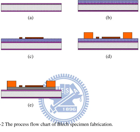
Two kinds of Blech specimens were fabricated, one being the Cu-Ni nanocomposite and the other being pure Cu. A 600nm-thick SiO2 insulating
layer was thermal grown on the silicon wafer and then a sandwich layer of Ti (2μm) /Cu (120nm) /Ti (5nm) was deposited by e-gun evaporation. The 2μm-thick Ti layer is served as the base conducting line of Blech structure and the Cu layer is the seed layer for electroplating. The 5nm-thick Ti layer needed in the nanocomposite case is for adhesion with the photoresist AZ10XT which is demanded for following electroplating in the alkaline copper plating solution. Afterward the test stripe regions were patterned photolithographically and then the ~1μm-thick Cu-Ni nanocomposite stripes and pure Cu stripes for two kinds of specimens respectively were electroplated. The test stripe patterns were designed in width of optimization with two different lengths which are 30 and 1000μm. Then the 5μm-thick Cu pads were patterned and electroplated for probing. Thus, the Cu and 2μm-thick Ti layers were photolithographically etched to form the Cu-Ni nanocomposite or pure Cu stripes on Ti base line, the Blech structure. Additionally we used surface roughness & profile meter ET-4000 to measure the accurate values of thickness of the test stripes for following accuracy of stress current density. Then, the Ni weight percentage in Cu matrix of the nanocomposite stripes was quantified to be 2.03% by inductively coupled plasma mass spectrometer (ICP-MS). Finally, a 1μm-thick SiO2 film was formed by plasma-enhanced CVD passivating the stripes from
oxidation during testing and we photolithographically opened the pads for probing. Fig. 2-2 depicts the process flow of electromigration Blech specimen fabrication and Fig. 2-3 shows the top-view scanning electron microscopy (SEM)
8
image of the fabricated Cu-Ni nanocomposite Blech specimen.
(a) (b)
(c) (d)
(e)
Fig. 2-2 The process flow chart of Blech specimen fabrication. (a) 0.6μm thermal grown wet oxide for insulation.
(b) Deposit Ti (2μm) /Cu (120nm) /Ti (5nm for Cu-Ni nanocomposite case) by E-gun evaporation.
(c) PR pattern test stripe region (AZ4620 for pure Cu sample and AZ10XT for Cu-Ni sample), electroplating test stripe.
(d) Electroplating Cu pads for about 5μm.
(e) Use PR JSR110N as mask, etching down Cu and Ti layer till oxide. Remove JSR110N, etching Cu seed layer
9
Fig. 2-3 Top-view SEM image of the fabricated Cu-Ni nanocomposite Blech specimen.
Electromigration test was done on an integral hot plate with the desired temperature and conducting the stress current by probing. Most of the current drifted into the test stripes because of the much larger resistance of the Ti base line than the test stripes. Percentage of the stress current detoured into the test stripes was estimated to decide the stress current density in the stripes. Optical microscope, scanning electron microscope (SEM) and focused ion beam (FIB) were utilized to observe the electromigration phenomena as well as measure the average depletion length and hence get the average drift velocity of the metal atoms.
10
Chapter 3 Results
3.1 Process Optimization of Cu-Ni Nanocomposite
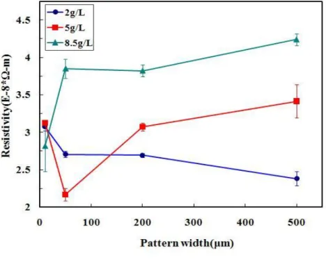
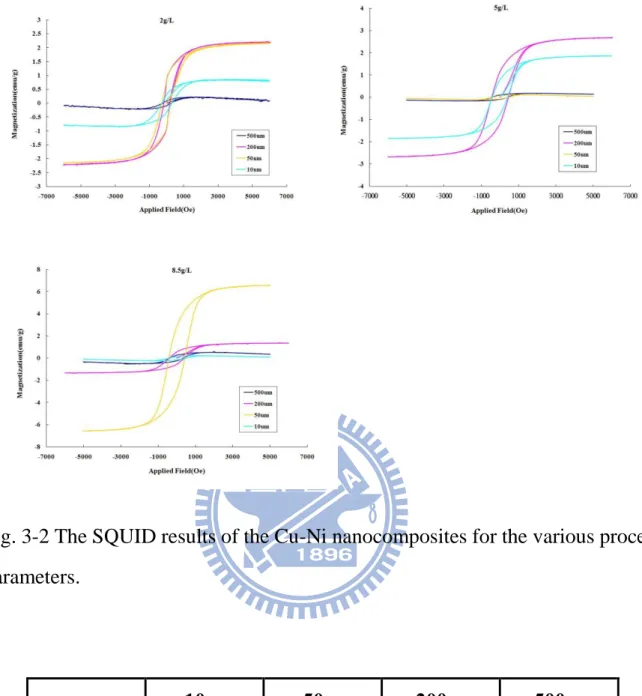
Fig. 3-1 shows the DC resistivity with respect to the aforementioned process parameters measured on a four-point probe station. Line width of 50μm plated in the bath with 5 g/L Ni powder concentration exhibits the best conductivity among other parameters. Fig. 3-2 shows the superconducting quantum interference device (SQUID) measurements of Cu-Ni nanocomposites with these parameters. Relative permeability of the composites μr,composite can
be obtained from the hysteresis loop by calculating the largest slope before the curve becomes saturated as follow,
(6)
where M and H are magnetization of the material and applied magnetic field respectively in the same unit. The calculated μr,composite values of the varied
11
Fig. 3-1 The DC resistivity of the Cu-Ni nanocomposites with respect to different process conditions. The resistivity of conventional pure Cu was also measured to be 1.88×10⁻⁸ Ω-m for comparison.
As previously proposed [1], the ratio in terms of power consumption
between the magnetic microactuators using pure Cu and nanocomposite coils respectively for the same output force,
(7)
where Pcomposite and Pc are the power consumptions of the magnetic
microactuators using nanocomposite and pure Cu coils respectively, and km and
kc are the electrical conductivities of the Cu matrix and composite films
12
Fig. 3-2 The SQUID results of the Cu-Ni nanocomposites for the various process parameters.
10μm 50μm 200μm 500μm
2g/L 1.132 1.318 1.323 1.037
5g/L 1.275 1.026 1.393 1.031
8.5g/L 1.046 1.435 1.198 1.091
13
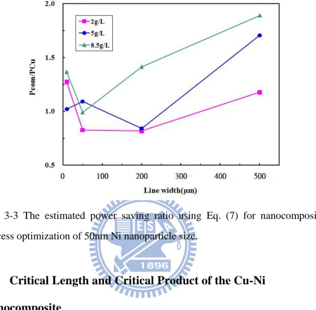
Substituting the data of DC resistivities and the calculated μr,composite values
into Eq. (7) with the μr,Cu being 0.999 conventionally, we have the power saving
ratios in terms of four different line widths with three different concentrations of 50nm Ni powders in the plating bath as depicted in Fig. 3-3. Previous work of 100nm Ni nanoparticles embedded in Cu matrix proposed an estimated 9% power consumption reduction with 200μm line width electroplated in the bath of 2 g/L Ni powder concentration [2]. For 50nm Ni nanoparticle size, Fig. 3-3 shows that 50, 200 and 200μm line width plated in the bath of 2, 2 and 5 g/L Ni powders respectively are estimated to be about 17% power saving, greater than the optimized process using 100nm Ni nanopowder. Thus, we used the process conditions, of which the 50μm line width and the 2 g/L concentration of 50nm Ni nanopowders in plating bath were chosen, to fabricate the electromigration testing Blech specimens. The reason not choosing line width of 200μm is that the huge current (~2 Ampere) needed to cause electromigration phenomena would burn the test structure because of joule heating.
14
Fig. 3-3 The estimated power saving ratio using Eq. (7) for nanocomposite process optimization of 50nm Ni nanoparticle size.
3.2 Critical Length and Critical Product of the Cu-Ni
Nanocomposite
Fig. 3-4(a) and (b) show the SEM images of the pure Cu and Cu-Ni
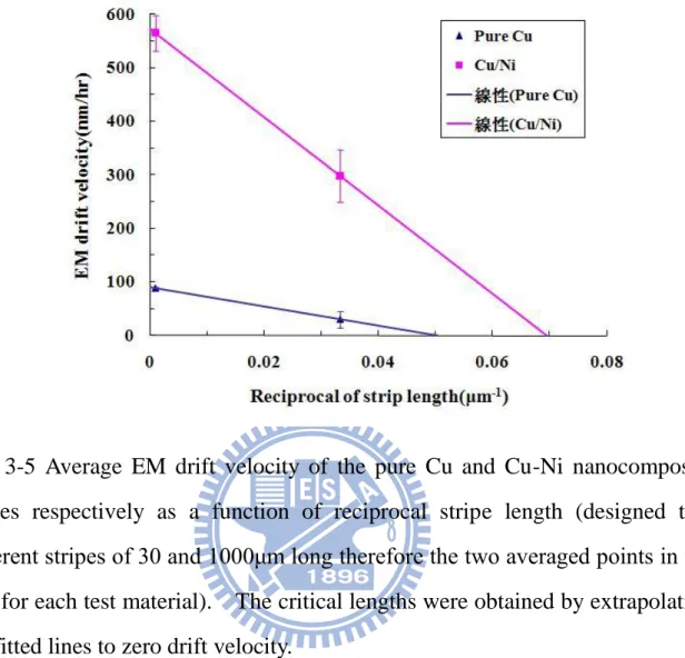
nanocomposite 1000μm-long stripes respectively at the cathode end before electromigration test. Fig. 3-4(c) and (d) show, after current stressing by 1.19×10⁶ A/cm2 at 275 C for 312 h, the corresponding SEM images to Fig. 3-4(a) and (b), respectively. Fig. 3-5 displays the average drift velocity of the Cu-Ni nanocomposite and pure Cu stripes respectively as a function of reciprocal of stripe length with stress current density 1.19×10⁶ A/cm2 at 275 C. As in the figure, the electromigration drift velocity decreases with increase of reciprocal stripe length, i.e. decrease of stripe length, the obvious effect of back
15
stress. The critical lengths were obtained to be about 20 and 14μm for pure Cu and Cu-Ni nanocomposite stripes respectively by extrapolating the fitting lines to the zero drift velocity and taking reciprocal of the x-axis interceptions. The shorter critical length of the Cu-Ni nanocomposite stripe means the more easily electromigration-induced depletion and extrusion for the same stripe length. By multiplying the acquired critical lengths with the stress current density, we obtained the critical product of about 2365 and 1714 A/cm at 275 C for the pure Cu and nanocomposite stripes respectively. Through the value of critical product, we can estimate the threshold current density, when the length of line segment was designed to be 1000μm at temperature condition 275 C, to be about 2.37×10⁴ and 1.71×10⁴ A/cm2 for pure Cu and composite respectively. These values represent the maximum current densities that the pure Cu and Cu-Ni nanocomposite can carry without electromigration damage at the above conditions.
16
(a) (b)
(c) (d)
Fig. 3-4 (a) and (b) are top-view SEM images at the cathode side of the 1000μm-long stripes of the pure Cu and the Cu-Ni nanocomposite Blech specimens respectively before current stressing. (c) and (d) are SEM images after current stressing by 1.19×10⁶ A/cm2 at 275 C for 312 h with respect to (a) and (b). The depletion edge is shown in (c) but is out of the image region in (d). The SEM images were taken after removing the SiO2 layer of passivation.
17
Fig. 3-5 Average EM drift velocity of the pure Cu and Cu-Ni nanocomposite stripes respectively as a function of reciprocal stripe length (designed two different stripes of 30 and 1000μm long therefore the two averaged points in the plot for each test material). The critical lengths were obtained by extrapolating the fitted lines to zero drift velocity.
3.3 Activation Energy of the Cu-Ni Nanocomposite
The average drift velocity of the metal atoms due to electromigration, as given by Huntington and Grone [9], is
(8)
where J is the atom flux, C is the density of metal ions, D is the diffusivity, D/kT is the mobility, k is Boltzmann’s constant, T is the absolute temperature, Z*e is
18
the effective charge of the ions, j is the electrical current density, ρ is the metal resistivity, D0 is the prefactor of diffusivity and Ea is the activation energy of
diffusion.
Equation (8) can be rewritten as
(9)
Therefore, by measuring the drift velocity as a function of reciprocal temperature, we can determine the activation energy Ea of the diffusion process
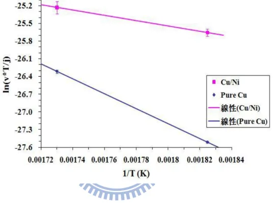
in electromigration. Fig. 3-6 shows the plot of ln(vT/j) as a function of the reciprocal temperature. The activation energies (Ea) can be determined from
multiplying the slopes of the fitted lines by minus of Boltzmann constant, i.e. “-”k, and their values are about 1.09 and 0.39 eV for pure Cu and Cu-Ni nanocomposite respectively in the temperature range of 275-305 C. The lower activation energy of diffusion is found for the Cu-Ni nanocomposite.
19
Fig. 3-6 Plot of the ln(vT/j) as a function of reciprocal temperature. Here the temperatures of 275 C and 305 C were chosen. The activation energies of pure Cu and Cu-Ni nanocomposite are 1.09 and 0.39 eV respectively, which were obtained from the slopes of the fitted lines.
20
Chapter 4 Discussion
4.1 Thermal Issue
Because of the larger resistivity of the Cu-Ni nanocomposite than pure Cu, the joule heat produced by the composite should be more than by pure Cu once power the stripes. There would be a doubt whether the practical temperatures are nearly the same in the Cu-Ni nanocomposite and pure Cu when current stressing. If they are far different, the comparison of the electromigration behaviors between the nanocomposite and pure Cu would be meaningless.
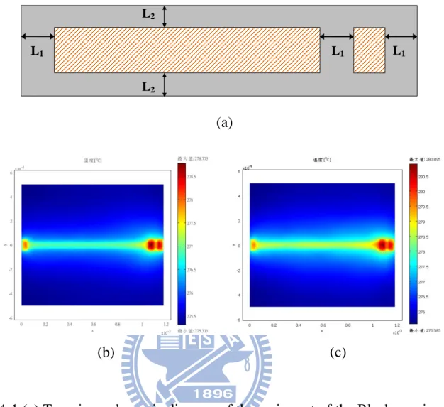
Fig. 4-1(a) shows the designed dimensions for the main part of the Blech specimen with test stripes of two different lengths on the Ti base line. Fig. 4-1(b) and (c) show the temperature distributions during electromigration test using heat transfer module of COMSOL Multiphysics simulation for pure Cu and Cu-Ni nanocomposite Blech specimens respectively. These two simulation structures were designed the Ti conducting baselines being directly on the silicon substrate, ignoring the 0.6μm-thick SiO2 layer between them. In
practice, this oxide layer would degrade thermal conducting by much lower value of thermal conductivity, and therefore make the simulations inaccurate. Thus, we estimate the Joule heat produced by the Blech specimens during current stressing per unit time and see if this oxide layer could conduct it according to the simulated temperatures in Fig. 4-1(b) and (c).
21
(a)
(b) (c)
Fig. 4-1 (a) Top-view schematic diagram of the main part of the Blech specimen indicates the designed dimensions. The test stripes represented by the oblique-line regions, of 30 and 1000μm long and 50μm wide, are on the Ti base line, where L1 = 50μm and L2 = 25μm.
(b) The temperature distribution diagram of thermal simulation for the main part of the Blech specimen of 0.7μm-thick pure Cu stripes on the silicon substrate with the bottom temperature of 275 C in the air, when the stress current is 0.5 Ampere. The resistivity of pure Cu is set 1.88×10⁻⁸ Ω-m.
(c) The temperature distribution diagram of thermal simulation with the same structure dimensions and thermal conditions as (b), except for the Cu-Ni nanocomposite stripes of 0.82μm thick and stress current being 0.64 Ampere. The resistivity of the Cu-Ni nanocomposite is set 2.71×10⁻⁸ Ω-m.
L1 L1 L1
L2
22
For the pure Cu Blech specimen, the total resistance of the two stripes on the Ti baseline is calculated by substituting the resistivities of pure Cu and Ti for 1.88 and 43×10-8 Ω-m respectively, the thicknesses of pure Cu stripe and Ti baseline for 0.7 and 2μm respectively and the structure dimensions depicted in Fig. 4-1(a). Then the power is gotten by multiplying the total resistance by square of the 0.5 Ampere stress current, as a result, to be ~191 mWatt. The equation of thermal conducting is as follow,
(10)
where dQ/dt is heat conducted per unit time, k is thermal conductivity of the mediate material, A is surface area conducting heat and ΔT/L is the temperature gradient between the two surfaces of the material. We set the k value of SiO2
to be 1.4 in units of W/m-K, the A value from Fig. 4-1(a) to be 0.118 mm2, ΔT from Fig. 4-1(b) to be 4 K and L to be 0.6μm. Thus the conducting heat rate in these conditions was calculated to be ~1.101 Watt, much greater than the Joule heating power produced by the current-carrying metal lines. In the same way, for the Cu-Ni nanocomposite Blech specimen in Fig. 4-1(c), the Joule heating power produced by the current-stressing structure is estimated to be ~345 mWatt, and the rate of heat conducting through the SiO2 layer is calculated using Eq. (10)
with ΔT = 6K as depicted in the right-hand temperature bar in Fig. 4-1(c), to be ~1.652 Watt. This argument proved that the simulated temperatures in Fig. 4-1(b) and (c) are close to the practical testing situation and the maximal temperatures of the two specimens under testing are about 2 C different, an insignificant influence on electromigration phenomena.
23
4.2 Surface Roughness Issue
(a) (b)
Fig. 4-2 (a) Cross-sectional FIB image of the Cu-Ni nanocomposite 1000μm-long-stripe cathode end after electromigration test. (b) Cross-sectional FIB image of the same stripe as (a) near the depletion edge, where the upper SiO2 layer, middle Cu-Ni nanocomposite film and bottom Ti
baseline were indicated in the image.
Fig. 4-2(a) and (b) show the cross-sectional focus ion beam (FIB) images
of the Cu-Ni nanocomposite 1000μm-long stripe after electromigration test at the cathode end and near the depletion edge respectively. The Cu-Ni nanocomposite film started voiding from the interface with the upper SiO2 layer
as indicated in the Fig. 4-2(b). Fig. 4-3(a) and (b) show the cross-sectional FIB images of the as-fabricated pure Cu and Cu-Ni nanocomposite Blech specimens respectively and Fig. 4-3(c) and (d) show higher magnification of FIB images corresponding to Fig. 4-3(a) and (b) respectively. We can see from Fig. 4-3(a) and (c) that the pure Cu film contacts smoothly with the upper SiO2 layer but
24
from Fig. 4-3(b) and (d) there are voids at the interface between the Cu-Ni nanocomposite film and the oxide layer.
The reason why these voids emerged at the interface in the nanocomposite case would be the result of the rougher surface of the Cu-Ni nanocomposite film. Fig. 4-4(a) and (b) show the surface morphology of the pure Cu and Cu-Ni nanocomposite film respectively measured by atomic force microscopy (AFM). The average surface roughness (Ra) of the pure Cu and composite are about 24 and 87nm respectively by AFM analysis. The larger Ra value of the nanocomposite film is supposed to be caused from the electroplating process, which was done under ultrasonication.
25
(a) (b)
(c) (d)
Fig. 4-3 (a) and (b) Cross-sectional FIB images of the pure Cu and the Cu-Ni nanocomposite Blech specimens respectively. (c) and (d) Enlarged images of (a) and (b) respectively. The specimens cut by FIB are before electromigration testing.
26
(a) (b)
Fig. 4-4 (a) and (b) AFM surface morphology measurements of the pure Cu and Cu-Ni nanocomposite film respectively.
C. L. Liu et al. have proposed the embedded atom method (EAM) for calculating the activation energy of surface diffusion on {100} surface of copper to be 0.38 eV [12]. Experimental study proposed by M. Breeman and D. O. Boerma for this same plane using low-energy ion scattering (LEIS) gave the value of 0.39 ± 0.06 eV [13]. Here the measured activation energy of diffusion of the Cu-Ni nanocomposite stripe capped by oxide passivation is ~0.39 eV, lying in the range of values obtained theoretically and experimentally for surface diffusion on copper. This result suggests that surface diffusion is the primary damage mechanism for electromigration in the Cu-Ni nanocomposite stripe. B. H. Jo and R. W. Vook have reported that under free surface and ultra-high vacuum conditions, the copper films exhibited surface diffusion mechanism on electromigration test [14], suggesting that in this study the voids at the interface between the Cu-Ni nanocomposite stripes and the oxide layer made the composite film a similar situation. For comparison, the measured activation energy of pure Cu is ~1.09 eV, indicating grain-boundary diffusion mechanism
27
under electromigration according to the values acquired for grain-boundary diffusion in copper.
28
Chapter 5 Conclusion and Future Work
The electroplated Cu-Ni nanocomposite film for low power magnetic microactuation application has been optimized with the process conditions which are 50μm-wide line pattern with the copper plating solution of 2 g/L 50nm-Ni-nanopowder concentration for accomplishing a power saving ratio of ~17%. Based on the optimized process parameters, the Cu-Ni nanocomposite Blech specimen, as well as the pure Cu one, are designed and fabricated to investigate the electromigration behaviors. The degraded activation energy of the composite in comparison with that of Cu is supposed to be resulted by the void formation at the interface between the composite film and the oxide cover. The imperfect interface is caused by the surface roughness (Ra) increase of the Cu-Ni nanocomposite film surface with respect to the pure Cu one. Owing to the large value of Ra for the composite originated from the electroplating process, the future work would be continuing on the surface morphology improvement of the Cu-Ni nanocomposite film for better electromigration resistance.
29
References
[1] Y. W. Huang, T. Y. Chao, C. C. Chen and Y. T. Cheng, APPLIED PHYSICS LETTERS 90, 244105 (2007).
[2] Y. C. Chen, W. T. Liu, T. Y. Chao and Y. T. Cheng, 15th International Conference on Solid-State Sensors, Actuators and Microsystems, Transducers 2009, Page 25-8.
[3] Yuanbo Li and Zhibin Jiang, Handbook of Performability Engineering, 58, 953-966 (2008).
[4] Thor Ansbaek, Dirch H. Petersen, Ole Hansen, Jakob B. Larsen, Torben M. Hansen and Peter Boggild, Microelectronic Engineering 86, 987-990 (2009). [5] J. H. Lin, K. Kuk, S. J. Shin, S. S. Baek, Y. J. Kim, J. W. Shin and Y. S. Oh,
Microelectronics Reliability 45, 473-478 (2005).
[6] K. Grenier, D. Dubuc, B. Ducarouge, V. Conedera, D. Bourrier, E. Ongareau, P. Derderian and R. Plana, 18th IEEE International Conference on MEMS, MEMS 2005 MIAMI: TECHNICAL DIGEST, 155-158 (2005).
[7] A. Deutschinger, U. Schmid, M. Schneider, W. Brenner, H. Wanzenböck, B. Volland, Tzv. Ivanov and I. W. Rangelow, Microsystem Technology 16, 1901-1908 (2010).
[8] K. N. Tu, Journal of Applied Physics, Vol. 94, No. 9 (2003).
[9] H. B. Huntington and A. R. Grone, Journal of Physics and Chemistry of Solids 20, 76 (1961).
[10] I. A. Blech, Journal of Applied Physics 47, 1203 (1976).
[11] I. A. Blech and C. Herring, APPLIED PHYSICS LETTERS 29, 131 (1976). [12] C. L. Liu, J. M. Cohen, J. B. Adams and A. F. Voter, Surface Science 253,
30
[13] M. Breeman and D. O. Boerma, Surface Science 269/270, 224-228 (1992). [14] B. H. Jo and R. W. Vook, Thin Solid Films 262, 129-134 (1995).
31