國立交通大學
加速器光源科技與應用學程 (材料組)
博士論文
鉍鐵氧化物薄膜之製備及特性研究
Physical characteristics and fabrication of BiFeO
3ferroelectric
thin films
研究生 : 劉晏廷
指導教授 : 陳三元 博士
共同指導教授 : 李信義 博士
鉍鐵氧化物薄膜之製備及特性研究
Physical characteristics and fabrication of BiFeO
3ferroelectric
thin
films
研究生 : 劉晏廷 指導教授 : 陳三元 博士 共同指導教授 : 李信義 博士 國立交通大學 加速器光源科技與應用學程 (材料組) 博士論文 A DissertationCollege of Engineering, National Chiao Tung University, Submitted to the Graduate Faculty
Of the
National Chiao Tung University
of Graduate Program for Science and Technology of Accelerator Light Source by
Yen-Ting Liu
In partial fulfillment of the Requirements For the Degree of
DOCTOR OF PHILOSOPHY June 2014
鉍鐵氧化物薄膜之製備及特性研究
研究生:劉晏廷 指導教授:陳三元 博士 李信義 博士 國立交通大學加速器光源科技與應用博士學位學程(材料組) 摘要 本論文在研究多鐵性鐵酸鉍(鉍鐵氧化物)材料之晶體結構與鐵電特 性。首先我們利用射頻磁控濺鍍系統成長單層之鐵酸鉍薄膜於鍍有鎳酸鑭 (導電材料)緩衝層之矽 (001) 單晶基板上。由高解析之X光繞射量測分析 得知,其薄膜沿著(001)面擁有高度優選指向之方向性。在成長溫度範圍為 400-600 o C,隨著成長的溫度提高其結晶性也跟著變佳。根據X光反射率的 擬合分析結果顯示,鐵酸鉍薄膜的密度較塊材小了些許。其殘留極化值隨 著成長溫度的提高而提升,此與X光繞射分析之結果相互印證,由此得知 鐵電特性與結晶性及電子密度有著正相關性。此實驗結果我們得知:鐵酸 鉍薄膜的鐵電特性大小的主要貢獻來自於其薄膜結晶性。 根據第一個研究主題結果顯示:對於鐵電薄膜材料而言,其薄膜的結 晶性是一項相當重要的議題;為了提升鐵酸鉍薄膜之鐵電特性,成長具有 磊晶品質的薄膜為一適當的研究方向。因此第二個研究主題是利用射頻磁 控濺鍍系統,成長具有對稱性結構鐵酸鉍/鎳酸鑭之人工超晶格磊晶薄膜於 鈮摻雜鈦酸鍶的單晶基板上。超晶格薄膜包含了 6-30 個週期,其單一層厚度為 1.7-8.5 奈米,而總膜厚則固定在 100 奈米,其成長溫度範圍為 560-810 o C,實驗結果顯示此超晶格結構之薄膜具備了令人滿意的結晶結構及應變效 應。此種鐵電材料與導電材料所形成之超晶格,可做為探討在單一超晶格 結構內,應變對於鐵酸鉍薄膜層之鐵電特性的影響。利用高解析之X光繞 射實驗,顯示除了主要的繞射峰兩側外皆有顯著的衛星峰;以及由X光反 射率曲線之 Kiessig 干涉條紋中可明顯分辨出超晶格之特徵峰,證實此濺 鍍薄膜確實具有超晶格結構。此薄膜的層狀結構亦由X光反射率、飛行時 間二次離子質譜儀及高解析穿透式電子顯微鏡分析得到確認,而且所有的 實驗皆得到一致性結果。在所有的成長溫度及不同疊層厚度下,超晶格薄 膜在其鈦酸鍶(002)布拉格繞射峰周圍皆有顯著的主繞射峰與衛星峰,代表 著於鈦酸鍶基板上可形成高品質之鐵酸鉍/鎳酸鑭人工超晶格結構。由高解 析之X光繞射量測結果得知無論是提高沈積溫度或是減少疊層厚度,皆會 提升其超晶格薄膜之結晶性,並沿著 c 軸方向有著拉伸應力以及沿著試片 表面有著壓縮應變的存在。 超晶格薄膜之殘留極化值顯示出與單層鐵酸鉍薄膜具有相同的趨勢; 其極化值隨著沈積溫度的增加而增加,在溫度 660 o C 時達到最大值。在量 測頻率為 0.5 及 1 千赫茲時,遲滯曲線顯現出極大的漏電流存在;極化值 隨著量測頻率的增加而減少。 因射頻磁控濺鍍系統有著先天上的物理極限,因此在最後的研究主題
裡我們利用原子層沈積系統,成長厚度小於 10 奈米,具有高度(001)優選 指向之超薄鐵酸鉍薄膜於鎳酸鑭緩衝層之矽(001)基板上,同時我們也利用 射頻磁控濺鍍系統成長相同厚度之樣品作為對照。結合了氣流中斷及鉍與 鐵前驅物之交替式反應,使原子層沈積系統為一優越成長三元化合物之方 法。根據X光繞射分析,在沈積溫度低於 550°C 時所生成的相只有鐵酸鉍。 藉由同步輻射X光繞射異常精細結構光譜,透過鐵酸鉍(001)繞射訊號可以 確認其鍵結之價數。利用X光光電子能譜術可得到其薄膜之成分比,結果 顯示利用原子層沈積法所成長之鐵酸鉍成分計量比射頻磁控濺鍍法來的正 確,並符合繞射異常精細結構之結果。利用高解析穿透視電子顯微鏡影像 鑒別薄膜之層狀結構與表面形貌,由原子層沈積法所成長之薄膜呈現相當 程度的覆蓋範圍,且較射頻磁控濺鍍系統來的一致性。因此利用原子層沈 積法所成長出之鐵酸鉍薄膜具有絕佳的低漏電特性,與射頻磁控濺鍍系統 相比大幅的改善了一千倍之多,使得這種方法更適合用於製造鐵電隨機存 取記憶體元件。由遲滯曲線可得知最大的殘留極化值為 2
Pr
= 2.0μC cm−2 。Physical characteristics and fabrication of BiFeO
3ferroelectric
thin films
Student: Yen-Ting Liu Advisor: Dr. San-Yuan Chen
Dr. Hsin-Yi Lee
Graduate Program for Science and Technology of Accelerator Light
Source National Chiao Tung University
ABSTRACTTo study the crystal structure and ferroelectric properties of multiferroic material BiFeO3 (BFO), we first investigated the BFO thin film as a single layer
grown on a Si (001) substrate coated with LaNiO3 (LNO) with a RF magnetron
sputtering (RF-sputtering) system. The measurements of high-resolution X-ray diffraction (HRXRD) showed a highly orientated crystal structure along (001) direction. The crystal quality increases with increasing deposition temperature in a range of 400-600 oC; according to the fitted results of X-ray reflectivity (XRR),
the densities of BFO thin films were slightly less than their bulk values. Increasing the deposition temperature increases the remnant polarization, and is consistent with the results of XRD, indicating that the ferroelectric property has a positive relation with the crystal quality and electron density. The results indicate that the crystal quality dominates the ferroelectric property of BFO thin films.
According to the first theme, the crystal quality is an important issue of a ferroelectric material; an epitaxial thin film is a proper direction to improve the ferroelectric property of a BFO thin film. The second theme is about an artificial superlattice of multiferroic BFO and conductive LNO grown epitaxially, with a
RF-sputtering system, on a single-crystal substrate of (001) Nb-doped SrTiO3
(STO) in a range 560-810 oC. The superlattice structure contains the features of
a satisfactory crystal structure and the strain effect in a single thin-film structure. The superlattice contained 6-30 periods of symmetric BFO/LNO bi-layers with each layer of thickness 1.7-8.5 nm. The total thickness of the films was fixed at ~100 nm. A ferroelectric and conductive superlattice material serves for an investigation of the strain dependence of the ferroelectric properties of BFO layers in a superlattice structure. The formation of the superlattice structure is confirmed from the appearance of satellite peaks on both sides of the main peak from the HRXRD pattern. The appearance of superlattice peaks separated by Kiessig fringes in the XRR curve. The layer structure is confirmed with XRR, a time-of-flight secondary-ion mass spectrometer (TOF-SIMS), and a high-resolution transmission electron microscope (HRTEM). All results are consistent with one another. The clearly discernible main peak and satellite peaks on both sides of the substrate peak around the (002) STO Bragg peak indicate the high-quality BFO/LNO artificial superlattice structure formed on a STO substrate at all deposition temperatures and with various thicknesses of sublayer. HRXRD measurements showed that these superlattice films become subject to greater tensile stress along the c-axis and compressive strain in the in-plane direction, and possess increased crystalline quality with both increasing temperature of deposition and decreasing thickness of the sublayer.
The remanent polarization of the superlattice showed the same behavior as the single-layer BFO thin film; the polarization increases with increasing deposition and approaches a maximum at 660 oC. The hysteresis loops showed a
large current leakage at frequencies 0.5 and 1 kHz; the polarization decreases with increasing measuring frequency.
Because of the physical limitation of RF-sputtering, the final theme is about highly (001)-oriented ultrathin BiFeO3 films of total thickness less than 10
nm deposited on Si (001) substrates via deposition of atomic layers (ALD) with a LaNiO3 buffer. A radio-frequency (RF)-sputtered sample of the same thickness
was prepared for comparison. The ALD, combined with interrupted flow and an exchange reaction between Bi and Fe precursors, provides a superior method to grow ternary compounds. According to X-ray diffraction, upon deposition at a temperature less than 550 °C, the only phase in the film is BiFeO3. Anomalous
fine structure from synchrotron X-ray diffraction certifies the valence bonding through the (001) diffraction signal. The stoichiometric ratio of BiFeO3 obtained
from X-ray photoelectron spectra indicates that ALD has a proportion much improved over the RF preparation, in agreement with the diffraction anomalous fine structure. The use of high-resolution transmission electron and atomic-force microscopes shows that the layer structure and morphology from ALD presented a satisfactory coverage, more conformal than that with the RF method. The BiFeO3 thin film deposited with ALD shows improved leakage at least 1000
times with respect to the RF preparation, making this method suitable for the fabrication of ferroelectric random-access memory devices. From the hysteresis loop, the largest remanent polarization is 2Pr = 2.0 μC cm−2.
致謝
首先我要感謝國家同步輻射研究中心 李信義博士,同時也是我的指導 教授。我在大學三年級時就已進入李博士的實驗室做專題研究,在當時受 到李博士的照顧也學到了許多。雖然沒有應屆考上研究所但李博士依然鼓 勵我再接再厲,隔年順利考上國立交通大學加速器光源科技與應用學程, 也進入李博士的實驗室做研究。李博士花費極大的心力在我身上,細心的 指導我,教導我實驗的方法、論文的寫作以及做人的態度,真的很感謝李 博士,沒有他就沒有我。也要感謝 陳三元博士,在這段時間大力的支持我、 指導我,讓我能順利完成我的博士論文。也要感謝 杜繼舜博士、黃嘉宏博 士、周振嘉博士以及林志明博士使得本論文的內容更加地圓融與充實,同 時也給我許多新的啟發。 此外要感謝 古慶順博士,在我的碩博士生涯給予我許多幫助與指導在 他身上學到研究的態度與新的思維,並且時常給予我適時幫助在我低潮時 給予我鼓勵與方向,讓我有動力繼續向前。也要感謝 劉恆睿博士與邱上睿 博士,在我剛進研究所時對一切都還很陌生,帶領我踏入這個未知的環境 讓我有所依靠,在此衷心的感謝。還要感謝實驗室的所有學弟妹的幫忙, 最後要感謝我的家人,在我求學階段一直以來對我的照顧與關心,讓我無 後顧之憂的專注於課業與研究上,謝謝您們。Contents 摘要……….. .i Abstract………...….iv 致謝………..………...vii Table Captions……….xi Figure Captions…………..………..……..xii Chapter 1 Introduction………....……….1
Chapter 2 Literature review……….……….6
2.1 Multiferroic material……….…………..……..……6
2.1.1 Ferroelectric properties………...6
2.1.2 Ferroelectric hysteresis loop and polarization switching………...8
2.2 Structure and physical properties of BiFeO3 (BFO)………11
2.2.1 Crystal structure of BFO………..……11
2.2.2 Physical properties of BFO………..12
2.3 Structure and physical properties of LaNiO3 (LNO)………….……..14
2.4 Structure and physical properties of SrTiO3 (STO)………16
Chapter 3 Experiments……….……..…………18
3.1 Deposition systems………...………18
3.1.1 High-vacuum RF Magnetron Sputtering System (HV RF-sputtering)………18
3.1.2 Ultrahigh-vacuum RF- Magnetron Sputtering System (UHV RF-sputtering)………..…..20
3.1.3 Atomic Layer Deposition (ALD)……….23
3.2 Characterization of structure……….26
Contents (continued)
3.2.2 Synchrotron Radiation X-ray Scattering (SRXRS)………..28
3.2.3 Atomic Force Microscope (AFM)...…….………34
3.2.4 High Resolution Transmission Electron Microscope (HRTEM)….36 3.3 Characterization of properties………...………37
3.3.1 Diffraction Anomalous Fine Structure (DAFS)..……….37
3.3.2 Time-of-Flight Secondary-ion Mass Spectrometer (TOF-SIMS)…38 3.3.3 X-ray Photoelectron Spectra (XPS)……….39
3.3.4 Ferroelectric Test System (FTS).……….40
3.3.5 Positive up and negative down (PUND).……….43
Chapter 4 Results and Discussion…..………44
4.1 Structure and physical properties of the single-layer BFO thin film..44
4.1.1 Crystal structure of the BFO thin film………..…………44
4.1.2 Electrical properties of the BFO thin film…….………...……53
4.2 Epitaxial growth and effect of strain on the BFO/LNO superlattice..56
4.2.1 Structure of the BFO/LNO superlattice………...………….56
4.2.2 Electrical properties of BFO/LNO superlattice……….…...75
4.3 Sublayer thickness and leakage effect of the BFO/LNO superlattice……….……….………..78
4.3.1 Crystal structure of the BFO/LNO superlattice with varied sublayer thickness………..………78
4.3.2 Electrical properties of the BFO/LNO superlattice with various sublayer thicknesses..……….……….85
4.4 Growth of ultra-thin undoubted BFO films by atomic layer deposition…..………..91
Contents (continued)
4.4.2 Leakage property of the ultra-thin BFO films………...99
4.4.3 Cross-sectional image and surface morphology of ultra-thin BFO films………...……101
4.4.4 Ferroelectric property of ultra-thin BFO films……….……..105
Chapter 5 Conclusions……….…….111
Table Captions
Table 3.1 The growth conditions of BFO/LNO superlattice : deposition temperature and sublayer thickness..………...21 Table 4.1.1 Parameters from best-fitted results of reflectivity curves of BFO
films deposited on the LNO-coated Si substrate at various temperatures..………..………...……….50 Table 4.2.1 Parameters obtained from best-fit results of reflectivity curves of
BFO/LNO superlattice films deposited on the Nb-doped STO substrate with varied deposition temperature………...……72 Table 4.3.1 Thickness parameters of the BFO/LNO superlattice obtained from
the results of X-ray diffraction, X-ray reflectivity and SIMS…….80 Table 4.4.1 Parameters obtained from best-fit results of XPS spectra of BFO thin
films deposited on the LNO-coated Si substrate by (a) ALD and (b) RF-sputtering………..…….………...…...….98
Figure Captions
Figure 2.1 Illustration of the changes in a ferroelectric material which transforms from a paraelectric cubic into ferroelectric tetragonal phase with
temperature.……….8
Figure 2.2 Ferroelectric (P –E) hysteresis loop. Circles with arrows represent the polarization states………..………....10
Figure 2.3 Crystal structures of BiFeO3; (A) tetragonal (B) unit cells…….…...11
Figure 2.4 (a) Crystallographic and (b)magnetic structure of BFO……….…...12
Figure 2.5 Polarization of BiFeO3: bulk single crystal (top) and epitaxial thin film (bottom)……….13
Figure 2.6 Structure of LNO crystal………....15
Figure 2.7 Structure of STO crystal………17
Figure 3.1 High vacuum RF-sputtering………...…………19
Figure 3.2 BFO/LNO superlattices………...………...22
Figure 3.3 Ultra high vacuum RF-sputtering………..……22
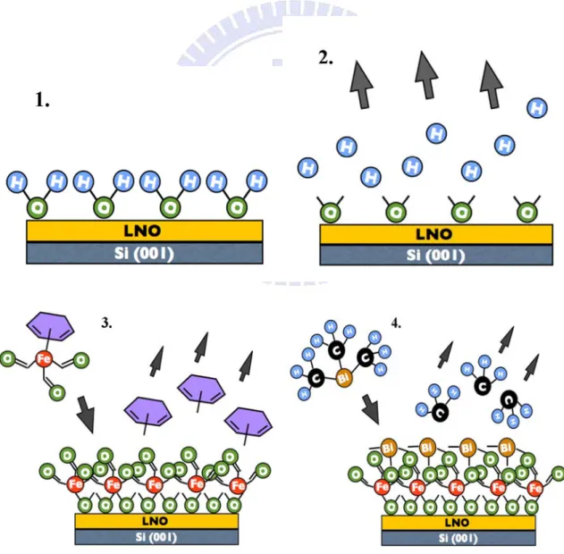
Figure 3.4 ALD deposition process of BFO thin film for one cycle.…………..24
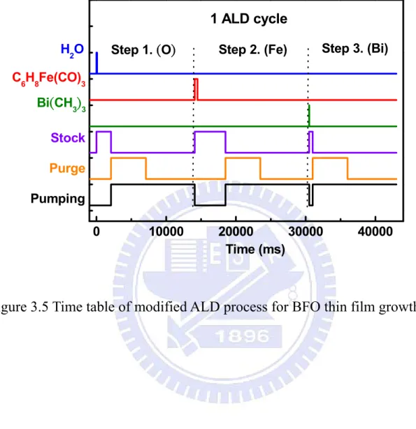
Figure 3.5 Time table of modified ALD process for BFO thin film growth…...25
Figure 3.6 X-ray diffraction and X-ray reflectivity……….27
Figure 3.7 Synchrotron Radiation………...29
Figure 3.8 Taiwan Light Source (TLS at NSRRC)………...30
Figure 3.9 Insertion device….………...……..33
Figure 3.10 NSRRC BL17b1 eight circle diffractometer………...33
Figure 3.11 Sketch diagram of AFM apparatus………..…35
Figure 3.12 TEM………..…...36
Figure 3.14 Excitation signal for a triangular voltage hysteresis measurement..41
Figure 3.15 Waveform of the leakage current measurement………..…42
Figure 3.16 Typical excitation of PUND measurement……...………..……….43
Figure 4.1.1 XRD “θ–2θ” scan of BFO films deposited on a LNO-coated Si substrate at various temperatures. The inset shows the width of the
BFO (002) rocking curve (ω scan)………...45 Figure 4.1.2 In-plane grazing-incidence XRD pattern of BFO films deposited on
a Si substrate at various temperatures……….46 Figure 4.1.3 X-ray reflectivity curve (open circle) of BFO films deposited on a
Si substrate at various temperatures and their best-fitted data (solid line) as a function of momentum transfer. The inset shows an expanded view of the best-fitted curve (solid line) and experimental data (open circles) of a BFO film deposited at 500 °C………..………...………..48 Figure 4.1.4 AFM images of single-layer BFO deposited on the LNO coated si
substrate at substrate temperatures/°C: (a) 300, (b) 400, (c) 500 and (d) 600……….49 Figure 4.1.5 Rocking-curve measurement of the BFO film deposited at 500 °C.
The arrows indicate two diffuse scattering peaks on the shoulder. The inset shows a comparison of intensity curves between specular and diffuse X-ray scattering...52 Figure 4.1.6 P–E hysteresis loops of BFO films (thickness 60 nm) deposited on
the LNO-coated Si substrate at various temperatures…...…...54 Figure 4.1.7 J-E curve of single-layer BFO thin films deposited at 300 – 700
°C………...…....55 Figure 4.2.1 Intensity distribution of the (002) radial scan of the BFO/LNO
superlattice film deposited at various substrate temperatures. The inset shows an expanded view of the superlattice film deposited at 660 °C……….…………..……….…...57 Figure 4.2.2 X-ray intensity of the radial scans along the (200) in-plane Bragg
peak of BFO/LNO superlattice films deposited at various substrate temperatures. An arrow marks the position of the superlattice main peak……….……...……58 Figure 4.2.3 Azimuthally scan (Φ scan) of the surface peak and the substrate Bragg peak for a superlattice film deposited at 660 °C……...…..60 Figure 4.2.4 Intensity distribution of the (111) radial scan of the BFO/LNO superlattice film deposited at 660 °C………..……...…….60 Figure 4.2.5 HRTEM cross-sectional images of the BFO/LNO superlattice on
the (001) SrTiO3 substrate deposited at 660 °C; (a) large scale
image, and (b) image of the interface regions between individual layers and between film and substrate………...……...61,62 Figure 4.2.6 DAFS result of the (002) superlattice diffraction peak and the extra
peak as shown in figure 4.2.1 (marked *) for film deposited at 710 °C (a) Ni K-edge, and (b) La L1-edge………...………64 Figure 4.2.7 In-plane compressive strain and out-of plane tensile strain of the
BFO layer as a function of deposition temperature…….…...….67 Figure 4.2.8 Rocking curves of the in-plane (200) main peak of BFO/LNO
superlattice films deposited at various temperatures...……...…..68 Figure 4.2.9 Reflectivity curves of BFO/LNO superlattice films deposited at
as a function of momentum transfer………70 Figure 4.2.10 AFM images of BFO/LNO superlattice films deposited at
substrate temperatures/°C: (a) 560, (b) 610, (c) 660, (d) 710, (e) 760, and (f) 810………....……..…...74 Figure 4.2.11 P-E hysteresis loops of BFO/LNO superlattice deposited at
various substrate temperature…………..……..…………...….76 Figure 4.2.12 J-E curve of BFO/LNO superlattice films deposited at 560 – 710
°C………..………...77 Figure 4.3.1 Intensity distribution of the (002) radial scan for the BFO/LNO superlattice with varied thickness of sublayer and periods. The inset shows the best fits (solid line) for the experimental XRD patterns for BFO/LNO superlattices at thicknesses 3.6 and 8.5 nm…………...…………..……….……….…..79 Figure 4.3.2 SIMS depth profile of the (BFO8.5/LNO8.5)6 superlattice film…....81
Figure 4.3.3 X-ray intensity of a set of radial scans along the (200) in-plane Bragg line of BFO/LNO superlattice films deposited for varied periods. An arrow marks the position of the superlattice main peak. The inset shows an azimuthal scan (Φ scan) of the surface peak and the substrate Bragg peak for a (BFO1.7/LNO1.7)30 superlattice
film………...83 Figure 4.3.4 Strain dependent and J–E curve of BFO/LNO superlattice films
with varied sublayer thickness (a) in-plane strain and out-of-plan strain, and (b) the J–E curve……….………86 Figure 4.3.5 P–E hysteresis loops of a BFO/LNO superlattice at thicknesses 1.7,
3.6 and 8.5 nm of sublayers and single-layer BFO thin film (thickness 60 nm)………..………..…..88
Figure 4.3.6 Polarization measurements for all sublayer thicknesses and a single- layer BFO (a) polarization value (2Pr) at varied frequencies from P–E hysteresis loops, and (b) the remanent polarization obtained from the PUPD test………...……….90 Figure 4.4.1 ALD growth rate as a function of substrate temperature for BFO
thin films deposited on the LNO-coated Si substrate………92 Figure 4.4.2 Surface normal radial XRD spectra of BFO thin film deposited at
various substrate temperatures……….……….94 Figure 4.4.3 DAFS results of BFO thin film deposited at 500 oC (a) Fe3+ K-edge,
and (b) Bi3+ L
3-edge………..…..…..………96
Figure 4.4.4 XPS spectra of BFO thin film by (a)-(c) ALD (d)-(f)
RF-sputtering………..………..98
Figure 4.4.5 J-E curves of the BFO thin films with different substrate temperatures………..…100 Figure 4.4.6 Cross-section view of HRTEM for BFO thin films grown on LNO
buffer layer by (a) ALD (b) RF-sputtering………..102 Figure 4.4.7 AFM images of BFO thin films grown by (a) ALD and (b)
RF-sputtering……….……….………104 Figure 4.4.8 P-E hysteresis loops of BFO thin film deposited in the range of
substrate temperature 480-550 oC…...…………...……….106
Figure 4.4.9 The relationship among crystal structure, leakage current, and
polarization at various deposition temperatures of ALD……...107
Figure 4.4.10 Normalized polarization as a function of film thickness grown by RF-sputtering, PLD, CVD, Sol-gel, and ALD this work………110
Chapter 1
Introduction
Multiferroic materials with a structure of perovskite type, in which ferroelectric and magnetism coexist, have attracted much attention, due to the physical properties that they offer prospective applications in devices taking advantage of two coupled parameters based on a local lattice distortion and electron spin [1-4]. Multiferroic oxide thin films are hence intensively investigated because of their scientific importance and technological promise for applications as non-volatile memories, such as ferroelectric random-access memories (FRAM), magneto-resistive random-access memories (MRAM) etc [4-8]. Among various multiferroic oxide materials, BFO has attracted much attention because of its high Curie temperature, TC = 1043 K, and high Néel
temperature, TN = ~647 K [9,10]. BFO possesses a large polarization and a low
crystallization temperature; both properties are desirable for highly dense FRAM. A randomly oriented ferroelectric capacitor tends to increase the variation of polarization bit to bit. As the material is free of lead, it becomes a worthy candidate for practical industrial applications. Ferroelectric thin films promise diverse applications in microelectronics and data-storage devices, such as sensors, transistors, and nonvolatile memories [11]. Considerable efforts have been focused on the deposition of BFO thin films with the most desirable film texture and electrical behavior for several technologically demanding applications, including RF magnetron sputtering, pulse-laser deposition (PLD), sol–gel synthesis, and chemical vapor deposition (CVD) [4,12-14]. PLD has been used to grow epitaxial superlattice films of complicated oxide materials. An advantage of this method is easily to control stoichiometry and crystal
structure etc. For this reason epitaxial superlattice films of complicated oxides are typically prepared by PLD at high temperature [15,16]. RF magnetron sputtering is also an important method to grow epitaxial perovskite oxide thin-film materials because of the great reproducibility of the chemical composition and the facile control of the process [17-19]. RF magnetron sputtering has the advantages of large throughput at low cost and a large uniform region of deposition; both properties match well the requirements of industrial applications. A randomly oriented ferroelectric capacitor tends to increase the variation of polarization. To decrease this variation, epitaxial films might be the best option [20]. Epitaxial superlattice thin films have demonstrated perfect ferroelectric properties that have advantages in scaling for highly dense ferroelectric memory devices [17].
Integrated circuits (IC) constitute an application in which improved materials are critically required. FRAM are electroceramics at the current state of the art in commercial electro devices, but many other IC designs might benefit from electroceramics in the future. To fulfill the requirements of the semiconductor industry and to introduce the multiferroic material into this field for FRAM in a new generation [3], growing a thin layer onto a wafer scale and conformal coverage with decreasing leakage properties for devices are urgent need. The improved method to process thin films, such as ALD, is an application for this purpose.
In this dissertation, the first part describes the fundamental properties of BFO thin films; BFO thin films were deposited on a LaNiO3-coated Si substrate
with a RF magnetron sputtering system. X-ray reflectivity and diffraction were used to characterize the microstructure of the crystal quality, buried interface, and surface morphology of BFO thin films. We used LNO because it is a
metallic material that can serve both as the bottom electrode in fabricating integrated ferroelectric capacitors on Si and an effective interface for the growth of highly oriented ferroelectric thin films [21- 24].
The second part is to explore how the substrate-induced strain affects the ferroelectric behavior of ferroelectric thin films. Epitaxial strains can greatly enhance the ferroelectric polarization and the Curie temperature of thin films relative to their bulk counterparts [25]. We fabricated BFO/LNO superlattice films on Nb-doped SrTiO3 (STO) substrate with an ultrahigh-vacuum RF
magnetron sputtering system to improve the crystal quality and electrical properties; Nb-doped STO can serve as the bottom electrode. The crystalline phases, interfacial structure, and morphology of thin films are important because they have strong impacts on physical properties and applications. As there exists little information on the microstructure and morphology of the interfacial structure of multiferroic superlattice thin films, the investigation of superlattice structure on a microscopic scale becomes highly significant for applications involving the dense memory in multiferroic materials [26].
Whereas X-ray diffraction at grazing incidence is a valuable analytical tool to characterize epitaxial thin films, X-ray reflectivity has been demonstrated to be a powerful tool to determine the thin film structure of the interfaces and surface morphology layer by layer. We used LNO (lattice parameter 0.3861 nm of pseudocubic unit cell) because it has a crystallographic compatibility for the heteroepitaxial growth of a BFO (lattice parameter 0.3962 nm of rhombohedral unit cell) layer; a lattice parameter smaller than that of BFO introduces a strain through a lattice mismatch at the interface [27-30]. In this superlattice system, the ferroelectric properties of the superlattice films result mainly from the ferroelectric layers, i.e., BFO, because of the conductive property of the LNO
material. For a ferroelectric and conductive superlattice thin film, those materials can therefore serve for an investigation of the strain dependence of ferroelectric properties of BFO layers in superlattice structures.
In the final part, the leakage current is a major problem in BFO thin films; to improve the leakage issue of the BFO thin films, ALD was first introduced to grow of BFO thin films. ALD is a self-limiting process to grow thin films that possess several practical advantages including accurate and simple control of the film thickness, larger grown area and larger batch capability, effective conformality, and reproducibility [31]. The convectional ALD process is highly suitable for the growth of binary compounds; only a few reports were published about ternary compounds with ALD [32-34], among which BFO is absent. The most straightforward approach for ALD of multicomponent oxides is to use separate binary cycles of deposition and to adjust the composition with a variation of the cycle ratio [35]. All cation precursors must be compatible, i.e. volatile, thermally stable and reactive at the same process temperature. These requirements yield a fairly narrow window of the process, which is just below the decomposition temperature of the least stable precursor. The bilayer structure of two binary compounds that are not true ternary compounds is due to poor valence binding between two cation atoms when the bilayer ratio is large [35]. For the purpose of preparing the ternary BFO, we implemented an ultra-rapid ALD diaphragm valve installed between the reactor and the vacuum pump in a novel ALD process, with interruption of the flow rate. To retain a precursor in the reactor chamber, the valve was closed first for a small interval before a precursor was introduced into the reactor [36]. The main influences of this step are to enhance the precursor density in the reactor and to extend the duration of the reaction at the sample surface, which provides a satisfactory condition to
grow thin films.
In this work, we report for the first time the highly (001)-oriented BFO thin films grown with the ALD on a Si (100) substrate with LNO buffer layer and the deposition temperatures are in a range of 480 - 550 oC, which shows satisfactory results for the crystal structures and ferroelectric properties.
Chapter 2
Literature review
2.1 Multiferroic materialMultiferroics or magnetoelectrics, have more than two switchable states such as polarization, magnetization and strain [37,38]. Multiferroics show multifunctional materials of an appealing class that exhibit several ferroic orders as ferroelectricity and antiferromagnetism at the same time [3]. The coexistence of several order parameters drives new physical phenomena and provide possibilities for novel device functions [39].
A multiferroic that is ferromagnetic and ferroelectric has demonstrated large linear magnetoelectric effects. As a result of the ferroelectric and ferromagnetic materials that typically possess large permittivity and permeability respectively, αij is bounded by the geometric mean of the
diagonalized tensors εii and μjj such that:
jj ii
ij
2 0 0 [40]
Both magnetization and polarization are indicated to encode information independently in a single multiferroic. A four-state memory has been demonstrated [41], but in reality it is agreed that the two order parameters are coupled [42,43]. Coupling could in theory allow data to be written electrically and read magnetically. It would take advantage of the best field of FRAM and magnetic data storage; this condition is attractive [3].
2.1.1 Ferroelectric properties
Ferroelectrics are polar materials that are provided with two equilibrium orientations of the spontaneous polarization vector in the absence of an external electric field, and in which the spontaneous polarization vector can be switched
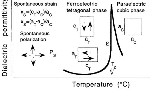
between those orientations with an electric field [44-46]. Most ferroelectric materials experience a phase transition of crystal structure from a high-temperature nonferroelectric phase into a low-temperature ferroelectric phase (Fgure 2.1). The paraelectric phase might be piezoelectric or non-piezoelectric and is rarely polar [44]. The symmetry of the ferroelectric phase is invariably less than the symmetry of the paraelectric phase. The temperature of the phase transition is called the Curie point (TC). Above the
Curie point the dielectric permittivity decreases with increasing temperature according to the Curie–Weiss law
0 0 0 T T C T T C
in which C is the Curie constant and T0 (T0 ≦ TC) is the Curie–Weiss
temperature.
Only a transition temperature into the first ferroelectric phase is called the Curie point. The transition into a ferroelectric phase generally leads to strong anomalies in the dielectric, elastic, thermal, and other properties [44], and is accompanied with changes in the dimensions of the unit cell [47].
Figure 2.1 Illustration of the changes in a ferroelectric material which transforms from a paraelectric cubic into ferroelectric tetragonal phase with temperature. The arrows show possible directions of the spontaneous polarizations (in two dimensions). The unit cells are represented by a square for the cubic phase and rectangle for the tetragonal phase [47].
2.1.2 Ferroelectric hysteresis loop and polarization switching
The most important characteristic of ferroelectric materials is the polarization switching with an electric field. One outcome of the domain-wall switching in ferroelectric materials is the occurrence of a ferroelectric hysteresis loop (Figure 2.2) [47]. This hysteresis loop can be observed experimentally with a Sawyer - Tower circuit [48]. With small values of an AC electric field, the polarization increases linearly with the field amplitude, according to relation
j ij
i E
This condition corresponds to segment AB in Figure 2.2. In this area, the field is insufficiently strong to switch domains with the unfavorable direction of polarization. With increasing field, the polarization of domains with an unfavorable direction of polarization begins to switch in the direction of the field; the measured charge density (segment BC) increases rapidly. The polarization response in this region is strongly nonlinear and the equation is no longer effective. In case all domains are aligned (point C), the ferroelectricity again becomes linear (segment CD). If the field intensity begins to decrease, some domains switch back, but at zero field the polarization is nonzero (point E). To measure a zero polarization state, the field must be reversed (point F). Further increased field in the negative direction causes a new alignment of dipoles and saturation (point G). The field strength is then decreased to zero and reversed to complete the cycle. The value of polarization at zero field (point E) is called the remanent polarization (Pr). The field required to cause the polarization to zero is
Figure 2.2 Ferroelectric (P –E) hysteresis loop. Circles with arrows represent the polarization states [47].
2.2 Structure and physical properties of BiFeO3 (BFO)
2.2.1 Crystal structure of BFO
The phase of BFO at 300 K is classified as rhombohedral (point group R3c) [49]. The unit cell of perovskite type has lattice parameter 0.3965 nm and rhombohedral angle of 89.3 – 89.48o [50,51], with ferroelectric polarization along [111] pseudocubic [51]. The unit cell is also describable in a hexagonal frame
of reference, with the hexagonal c-axis parallel to the diagonals of the perovskite
cube, i.e., [001]hexagonal ∥ [111]pseudocubic. In some cases, a pseudocubic
representation has been used, in which [111]c is equivalent to [001]hex. Oxygen
atoms occupy face-centered sites of the Bi cubic framework. The coefficient of thermal expansion is neither completely linear nor isotropic [52-54], and accounts of values [52,53] vary notably, ranging from 6.5×10⁻⁶ to 13×10-6 K-1. BFO is a material with a high ferroelectric Curie (TC=1083 K) [55] and
antiferromagnetic Neel (TN=643 K) [56] temperatures.
2.2.2 Physical properties of BFO
BFO has been reported to be ferroelectric with its polarization oriented along the rhombohedral c-axis [111]c due to the displacement of Bi, and Fe, O
relative to each other [57] shown in Figure 2.4(a); neutron diffraction experiments revealed antiferromagnetic ordering along [111]c [58]. Spins in
neighboring positions are antiparallel with each other, producing a G-type antiferromagnetic ordering, as presented in Figure 2.4(b).
Figure 2.4 (a) Crystallographic and (b) magnetic structure of BFO [59].
The early measurements of bulk ferroelectric materials in the 1960s and 1970s yielded only small values of the polarization, but the small value of Pr = 6
μC cm-2 reported by Teague et al [55]. for single crystals was viewed by those authors as limited without saturation. The greatest polarization of the thin films was initially thought [2] to be resulted from strain enhancement; great single crystals were grown finally [60-64], with Pr values near those of the films about
60 μC cm-2 normal to (001) orientation (Figure 2.25) and, therefore, near 100 μC cm-2 along [111]pseudocubic; a large polarization property was also discovered in
ceramics [65]. Calculations of electronic structure agree with the statement that the polarization of bulk BFO is intrinsically large [66,67] (90–100 μC cm-2) and insensitive to strain [67].
Figure 2.5 Polarization of BiFeO3: bulk single crystal (top) [60] and epitaxial
2.3 Structure and physical properties of LaNiO3 (LNO)
Among perovskite oxide materials of many kinds, LNO is an uncommon instance exhibiting paramagnetic metallic behavior. The interest in this material has led to the development of extremely conductive electrodes for ferroelectric thin-film devices, including nonvolatile memories for technological applications [68]. Superior heteroepitaxy with doped lanthanum manganites [69] means that LNO thin films can also serve as electrodes in magnetoelectronic devices in view of highly spin-polarized compounds [70,71].
LNO is a perovskite material with a distorted rhombohedral structure of rhombohedral angle of 60.41° and lattice parameter a=0.5461 nm. A pseudocubic lattice parameter of LNO is 0.383 nm is shown in Figure 2.6. LNO is n-type metallic oxide without doping. The oxide is characterized by a small electron density at EF like the new series of high Tc copper oxides [72]. The
resistivity at 300 K is about 1 mΩ.cm. The LNO single crystal can serve as a
metallic bottom electrode, an ohmic contact material, a conservatory metallic layer, and a lattice-matched metallic-oxide material.
2.4 Structure and physical properties of SrTiO3 (STO)
Strontium titanate (SrTiO3) has been variously used as a substrate to grow
oxide thin films of perovskite type, because STO is chemically and compositionally stable, and has a small lattice mismatch with many perovskite-oxide materials [74-76]. The electrical conductivity of STOis readily
controlled from a n-type semiconductor to metal-like conduction (up to 10−4 Ω cm), and even to superconductivity at temperature TC<0.3 K when Ti is partly substituted with Nb or La [78-81].
STO is a popular material of perovskite type with a cubic structure with lattice parameter of a=0.3905 nm. Because of its large relative permittivity and small dielectric loss, STO is applicable to electronic devices. The conductive Nb-doped STO substance with variable conductivity is not only used as a bottom electrode for the deposition of functional perovskite oxides [82-84] but also provides a possibility to fabricate fascinating and novel devices such as multilayer structure [85,86], superlattice [87], tunnel junctions [88], field-effect transistor [89], Schottky junction [90], and p-n junction [91,92].
Chapter 3
Experiments
3.1 Deposition systems3.1.1 High-vacuum RF Magnetron Sputtering System (HV RF-sputtering)
The single-layer BFO thin film for study of the fundamental physical properties was deposited with a HV RF-sputtering system. The deposition chamber was connected to a pumping system consisting of a turbomolecular pump of speed 500 L/min; the base pressure was kept at 1×10⁻⁶ Torr to avoid contamination during deposition. The sputtering target of BFO was prepared through a conventional solid reaction on sintering a calcined mixed powder in a stoichiometric molar ratio Bi : Fe : O = 1.2 : 1 : 3; the excess bismuth compensated for Bi volatilization during deposition [94]; the LNO target with standard atomic ratio La : Ni : O = 1 : 1 : 3 was prepared on sintering calcined La2O3 and NiO powders (99.99 % purity) with standard atomic ratio La : Ni : O
= 1 : 1 : 3 at 950 oC for 2 h. Highly pure working gas argon (99.9995 %) and reactive gas oxygen (99.9995 %) were controlled with mass-flow controllers (MFC) to maintain a stable flow rate with argon at 8 sccm and oxygen at 2 sccm. The MFC were precisely calibrated; the accuracy of the gas flow rate was within 2 %. The distance from the target to substrate was 140 mm; the working pressure was fixed at 1.5×10⁻² Torr for growth of thin film. The sputtering was performed at power density of 1 W cm-2; a LNO bottom electrode of thickness 50 nm was deposited on a (001) Si substrate at 500 oC. The BFO thin films were deposited on a LNO-coated Si substrate; the thickness of each sample was fixed at ~60 nm at a temperature in the range of 300-700 oC. With these parameters, the growth rate of deposited thin films of BFO is 1.37 nm/min.
The Si substrates were cleaned with supersonic rinsing with acetone and methanol for 10 min before deposition; the substrate was dried with nitrogen gas.
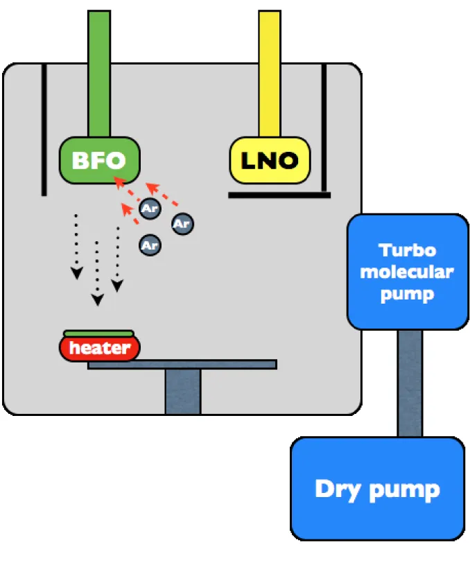
3.1.2 Ultrahigh-vacuum RF Magnetron Sputtering System (UHV RF- sputtering)
To grow a superlattice thin film of high quality, the UHV RF-sputtering system with a double gun was employed in this experiment. The vacuum chamber was connected to a pumping system comprising three turbomolecular pumps, two for the main chamber and one for the preparation chamber. The sample was transferred into the main chamber from the preparation chamber with a load lock; the shutter opening was controlled with a computer. We thereby controlled precisely the duration of deposition of each layer during the deposition of a superlattice thin film. The base pressure of the main chamber was kept at 3×10⁻⁸ Torr to avoid contamination at all times. The same sputtering target of BFO and LNO was used with the HV RF-sputtering. Highly pure working gas argon (99.9995 %) and reactive gas oxygen (99.9995 %) were also used and controlled with the MFC to maintain a stable flow rate with Ar at 8 sccm and O2 at 2 sccm. The distance from the target to the substrate is 90 mm;
the working pressure is fixed at 1.5×10⁻² Torr. The RF sputtering was performed at power density 0.74 W cm-2 (BFO) and 0.98 W cm-2 (LNO) without a bias voltage. The growth rate of thin films are 0.6 nm/min for BFO and 0.4 nm/ min for LNO; a shutter interrupts the deposition for 12 s between growths of consecutive sublayers. To design and optimize the growth condition of both the BFO/LNO superlattice and the thin-film structure for the electrical properties, we designed the superlattice to contain 30 periods of symmetric BFO/LNO with each sublayer of thickness 1.7 nm; the deposition temperature of the superlattice was set at 560, 610, 660, 710, 760 and 810 oC for the desired properties. Based on an optimum growth condition of the superlattice, a symmetric sublayer structure (BFOm/LNOm)n, in which m is the thickness/nm of sublayer and n is the number of repeating periods, was adopted to investigate the strain effect on the
ferroelectric properties. The superlattice structure contained BFO/LNO sublayers in 6-30 periods with a sublayer thickness in the range 1.7-8.5 nm at deposition temperature 660 oC. The total thickness of films was fixed at ~100 nm.
The STO substrate was cleaned with supersonic rinsing with acetone and methanol for 10 min, and subsequently heated at 710 oC for 10 min in a dioxygen atmosphere at 4×10⁻² Torr to clean the sample surface.
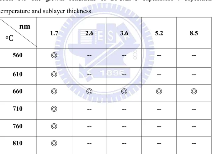
Table 3.1 The growth conditions of BFO/LNO superlattice : deposition temperature and sublayer thickness.
1.7 2.6 3.6 5.2 8.5 560 ◎ -- -- -- -- 610 ◎ -- -- -- -- 660 ◎ ◎ ◎ ◎ ◎ 710 ◎ -- -- -- -- 760 ◎ -- -- -- -- 810 ◎ -- -- -- -- o
C
nm
Figure 3.2 BFO/LNO superlattices.
3.1.3 Atomic Layer Deposition (ALD)
ALD is a self-limiting process to grow thin films that possess several practical advantages including accurate and simple control of thickness, large area, large batch capability, effective conformality, reproducibility, straightforward doping, scaling, ability to produce sharp, and tailored interfaces to prepare multilayer structures.[31]
ALD involves a self-limiting vapor-phase chemisorption that relies on consecutive surface reactions and utilizes critical purging steps to prevent interactions between reactive precursors.[95] The BFO thin films were grown on the LNO-coated Si (001) substrate with ALD; trimethylbismuth [(CH3)3Bi,
purity 95 % min, Nanjing Chemlin Chemical Industry Co., Ltd], cyclohexadieneiron tricarbonyl [C6H8Fe(CO)3; purity 97 % min, Alfa Aesar],
and deionized water (H2O) served as precursors for atoms of Bi, Fe and O,
respectively. Thin films of BFO were deposited to a desired thickness ~10nm in a range of 480 - 550 oC. A LNO buffer layer of thickness 50-70 nm was deposited on a Si(001) substrate at 500 oC with a RF-sputtering system, which provided a satisfactory condition for the growth of BFO.[96] Herein, a unique ALD process was adopted to grow the BFO thin film that differed from the conventional ALD process; the precursors were O, Fe, and Bi to form 1 ALD
cycle. The duration of pulses for O, Fe, and Bi were 100,400 and 15 ms,
respectively. Between a precursor pulse for evacuation of the chamber, the interval in which the ALD valve was closed to ensure that the precursor maintained a constant vapor pressure in the chamber so as to increase the reaction duration, we called the stock time [31,36], 2 s for O, 4 s for Fe, and 0.5 s for Bi. After the stock time, highly pure gaseous N2 (99.9995%) was employed
to purge the chamber for 5 s at 1.1 torr before being evacuated with a rotary pump for 7 s to base pressure 3x10⁻² Torr before the next precursor was admitted to the chamber, as shown in Figure 3.5. Purging and pumping were performed in the same manner as with the conventional ALD method. An enhanced affinity with a ferroelectric oxide had advantages for the interfacial properties between the conductive and ferroelectric oxides because of their similar structures of perovskite type provided by conductive oxides; the lattice parameter of LNO was a = 0.386 nm with a similar perovskite structure, which is compatible with the lattice parameter of BFO, a=0.396 nm [97].
0 10000 20000 30000 40000 Step 3. (Bi) Step 2. (Fe) Time (ms) H2O C6H8Fe(CO)3 Bi(CH3)3 Stock Purge Pumping Step 1. (O) 1 ALD cycle
3.2 Characterization of structure
3.2.1 X-ray Diffraction and X-ray Reflectivity (XRD & XRR)
X-ray diffraction is a powerful tool to determine the crystal structure and crystalline quality. For this XRD we used a rotating anode for Cu-Kα radiation in a commercial standard two-circle X-ray diffractometer (Max science M18XHF KXY-8019-1) operated at 50 kV and 200 mA in the X-ray laboratory at National Synchrotron radiation Research Center (NSRRC), Hsinchu, Taiwan. The XRD was measured with a 'θ-2θ' scan with scan speed 4o min-1 and scaling 0.02o. Techniques to analyze a thin film play an important role in industry to determine the characteristics of thickness, electron density, interface and surface roughness of thin films. The XRR technique involves the measurement of the radiation reflected from the interfaces and the surface of a multilayer structure that can provide information about the interface [98-101]. Relative to other methods to measure a surface, XRR yields a nondestructive measurement with high resolution from 0.1 nm 1 μm [102]. For XRR that is performed with a Huber two-circle diffractometer, we used the same X-ray source as for XRD. The incident light was made monochromatic with a flat Ge (111) crystal; two pair sets of slits served to eliminate Cu Kα2 contamination so yielding a
wave-vector resolution in the scattering plane of order 0.015 nm-1.
To derive the physical parameters of a superlattice, the simulation of specular reflectivity is based on the recursive formalism of Parratt [103]. The reflectivity curve is fitted with the BedeRERFS Mercury code [104] to determine
the physical parameters of the thin films, including the thickness of each layer, the electron density and the roughness of the surface or interface. This program calculates the reflectivity of the thin film with the dynamic Fresnel equations of
multilayer reflectivity, taking into account the absorption, instrumental resolution, interface roughness and abruptness and sample curvature.
3.2.2 Synchrotron Radiation X-ray Scattering (SRXRS)
A synchrotron is a cyclic particle accelerator of a particular type in which a magnetic field (to turn the particles so that they circulate) and an electric field (to accelerate the particles) are carefully synchronized with the traveling particle beam. With each turn in the accelerator, an accelerating RF voltage is applied to the charged particles. As the energy of the particles increases, so does the magnetic field of the ring, which maintains a constant radial orbit. Synchrotrons were originally developed by L. W. Alvarez for purposes of high-energy particle physics [105].
An accelerator takes stationary charged particles, such as electrons, and drives them to nearly the speed of light. In being forced by magnets to travel around a circular storage ring, charged particles emit electromagnetic radiation tangentially and, consequently, lose energy. This energy emitted in the form of light is known as synchrotron radiation. The synchrotron produces light on accelerating electrons almost to the speed of light. Magnets restrict the electrons to circular paths. As the electrons turn, photons (packets of radiant energy) are emitted. The infrared and UV light and X-ray are sent down pipes called beamlines, to work areas at which scientists conduct their experiments. The components of a synchrotron include an electron gun, linear accelerator, a circular booster ring (to increase the speed of the electrons), storage ring (to re-circulate electrons) and beamlines [105].
Figure 3.7 Synchrotron Radiation [105].
Basic Theory
Accelerated charged particles emit electromagnetic waves (radiations). A magnetic force is applied to the charged particles -- electrons or positrons -- to provide a central acceleration and to alter the trajectory of the charged particles. Radiation emits tangentially from the trajectory of the charged particles; its spectrum depends on the energy of the charged particles and the applied magnetic field. A RF cavity restores the lost energy of the charged particles and maintains a constant operating energy of the storage ring [105].
The properties of synchrotron radiation (SR) are high intensity and brightness (ISR > 106×Itube), a wide range of continuous spectrum (35 keV > E >
0.05 eV at NSRRC), excellent collimation, low emittance, a pulsed temporal structure, and polarization (linear or elliptical) and coherence [105].
The measurement of high-resolution X-ray diffraction (HRXRD) of the radial scan and grazing-incidence X-ray diffraction in plane (GIXRD) were performed at wiggler beamline BL-17B1 with a Huber eight-circle diffractometer at NSRRC, Hsinchu, Taiwan. With two pairs of slits between the sample and the detector, the typical scattering vector resolution in the vertical scattering plane was set to ~1×10⁻³ nm-1 in these experiments. The energy range is 4.8 ~ 14.2 keV, wavelength 0.087 nm ~ 0.25 m, energy resolution 2.2×10⁻⁴ , flux 2×10¹¹, spot size of full width at half maximum 0.6 mm (H) x 0.5 mm (V); the optics comprised a vertically collimating pre-mirror, a fixed-exit double-crystal Si (111) monochromator, a toroidal focusing mirror, and a scintillation counter as detector.
Although SR provides a strong and powerful X-ray source, in some experiments such as for analysis of a thin-film structure, great intensity and flux are urgently needed. An insertion device (ID), used for this purpose in the synchrotron facility, is a component in a modern synchrotron light source that has periodic magnetic structures that stimulate highly brilliant, forward-directed emission of synchrotron radiation on forcing a stored beam of charged particles to perform wiggles, or undulations, as they pass through the device. The Lorentz force causes this motion; from this oscillatory motion we derive the names for the devices of two classes -- wigglers and undulators. An ID is traditionally inserted into a straight section of a storage ring. As the beam of stored particles, generally electrons, pass through the ID, the alternating magnetic field experienced by the particles causes their trajectory to undergo a transverse oscillation. As there is little mechanical difference between a wiggler and an undulator, the criterion normally used to distinguish between them is the
mc qB K u 2
in which q is the charge of the particle passing through the ID, B is the maximum magnetic field of the ID, λu is the period of the ID, β = ν/c relates to
the speed, or energy of the particle, m is the mass of the accelerated particle, and
c is the speed of light. Wigglers are deemed to have K >> 1 and undulators to
have K < 1 [106].
As an insertion device in a synchrotron, a wiggler comprises magnets in a series designed to deflect laterally and periodically (wiggle) charged particles (invariably electrons or positrons) in a beam inside a storage ring of a synchrotron. These deflections create a altered acceleration that in turn produces emission of synchrotron radiation in a broad spectrum tangent to the curve, much like that of a bending magnet, but the intensity is greater because of the contribution of many magnet dipoles in the wiggler. Furthermore, a wavelength (λ) decreased means a frequency (ƒ) increased; this increased frequency is directly proportional to the energy, so that the wiggler creates a wavelength of light with a larger energy [107].
Figure 3.9 Insertion device [105].
3.2.3 Atomic Force Microscope (AFM)
An atomic-force microscope is a surface-sensitive technique for the surface science of thin-film materials. In a tapping mode, an AFM operates by scanning a tip approaching the end of an oscillating cantilever across the sample surface; the cantilever is driven to oscillate vertically near its resonance frequency with a small piezoelectric element mounted in the AFM tip holder similar to a non-contact mode. The amplitude of oscillation is greater than 10 nm, typically 100 to 200 nm. The interaction of forces acting on the cantilever when the tip approaches the surface -- van der Waals forces, dipole-dipole interactions, electrostatic forces, etc. -- cause the amplitude of this oscillation to decrease as the tip moves nearer the sample. A tapping AFM image is therefore produced on imaging the force of the intermittent contacts of the tip with the sample surface [108]. The feedback loop maintains a constant amplitude of oscillation on maintaining a constant RMS oscillatory signal acquired by the split photodiode detector. The vertical position of the scanner at each data point (x,y) to maintain a constant setpoint amplitude is stored in the computer to form the topographic image of the sample surface.
The surface roughness of the superlattice films of BFO/LNO/Si and BFO/LNO was observed with AFM (NT-MDT Solver P47H and Digital Instrument MultiMode) operated in a tapping mode with a silicon-nitride tip. The sample was fixed to an iron disk holder with double-side adhesive tape. The method to detect the cantilever deflection relies on optical interference. As the tip traces various surface features, its vertical movement shifts the laser beam between upper and lower photodiode components, creating voltage differences that are electronically converted into height information. The image is captured with a feedback-loop controller system. The scan rate of the tip was kept
constant at 0.3, 0.5 and 1 Hz; the scanned lines numbered 512; the z height was 500 nm, and the scan size was set at 1 x 1 μm2 and 2 x 2 μm2 .
3.2.4 High Resolution Transmission Electron Microscope (HRTEM)
For high-resolution transmission electron microscopy (HRTEM), an imaging mode of the transmission electron microscope allows for direct imaging of the atomic structure of the sample [109]. HRTEM is a powerful tool to study, on an atomic scale, the crystal structure of materials such as semiconductors, metals, nanoparticles and trigonal carbon, e.g. graphene, C nanotubes.
The layer structure and interface roughness of the single-layer BFO thin film and BFO/LNO superlattice are investigated with cross-sectional images from a HRTEM (JEOL JEM2010) to confirm layer and epitaxy of films.
3.3 Characterization of properties
3.3.1 Diffraction Anomalous Fine Structure (DAFS)
In general, X-ray scattering represents only information about the long-range ordering of atomic structure, but measurements of X-ray absorption fine structure (XAFS) provide short-range chemical information. DAFS combines all capabilities of XRD and XAFS in a single technique; it provides the advantages of information about short-range order of the set or subset of long-range ordered atoms selected by the diffraction condition [111]. DAFS is specific chemically and to valence, and is sensitive to the positions of neighboring atoms; atoms can be separated on measuring the DAFS intensities of Bragg peaks with varied diffraction structure-factor contributions. DAFS provides the same structural and spectral sensitivities as X-ray absorption near-edge structure, namely the valence, empty orbital and bonding information for the resonant atoms [112,113].
Measurement of DAFS was performed with a synchrotron source at wiggler beamline BL-17B1 with an eight-circle diffractometer at NSRRC, Hsinchu, Taiwan.
3.3.2 Time-of-Flight Secondary-ion Mass Spectrometer (TOF-SIMS)
Secondary-ion mass spectrometry (SIMS) is a technique used in material and surface sciences to analyze the composition of solid surfaces and thin films by sputtering the surface of the specimen with a focused beam of primary ions and collecting and analyzing the ejected secondary ions. The ratios of mass to charge of these secondary ions are measured with a mass spectrometer to determine the elemental or isotopic or molecular composition of the surface to a depth 1 - 2 nm. Because of a large variation in ionization probabilities among materials, SIMS is generally considered to be a qualitative technique, although quantization is possible with the use of standards. SIMS is the most sensitive technique for surface analysis, with limits of elemental detection ranging from parts per million to parts per billion [114].
The composition of the depth profile of the BFO/LNO superlattice was examined with a TOF-SIMS and a Cs+ ion source (12.5 keV with current 50 nA, CAMECA ims4f, in National Tsing Hua University). The raster size was 250 μm × 250 μm; the rate of sputtering was 0.06 nm s-1.
3.3.3 X-ray Photoelectron Spectra (XPS)
The chemical compositions of BFO thin films were measured with X-ray photoelectron spectra at a vacuum of 10-10 torr (PHI 1600 instrument). All XPS data were collected with Mg Kα X-rays at energy 1253.6 eV. The fits of XPS spectra were analyzed with software (XPSPEAK 4.1). The background was subtracted with a linear method and peaks were fitted with a mixed Gaussian-Lorentzian distribution. The atomic fraction of each element of the BiFeO3 films was calculated from the integrated intensity of signals and divided
by the relative sensitivity factor, for Bi-4f 9.14, for Fe-2p 2.957, and for O-1s 0.71. The integrated intensity of Bi-4f, Fe-2p and O-1s signals were calculated to obtain the content of Bi, Fe and O with this equation,
% 100 O Fe Bi i i I I I I C
in which i pertains to Bi, Fe or O, and Ci is the content of element i in the thin film.
3.3.4 Ferroelectric Test System (FTS)
Ferroelectricity is a property of a material that has a spontaneous electric polarization that becomes reversible on application of an external electric field [115,116]. The ferroelectric properties of the polarization – electric field (P-E) hysteresis loop of single-layer BFO thin films and BFO/LNO superlattice films were measured with a ferroelectric test system (TF Analyzer 2000 FE-Module, axiACCT Co.) at varied applied frequency in a range 1-5 kHz; the voltage was set at 5 or 6 V with applied current 1mA; a triangular waveform for samples near 300 K. The hysteresis measured the charge stored in a ferroelectric sample on integrating the current required to maintain one terminal of the sample at zero bias. On eliminating the external capacitor, the circuit decreased the effect of parasitic capacitor and allowed a highly accurate characterization of ferroelectric devices. Figure 3.13 shows a schematic diagram of the ferroelectric test system.
Figure 3.13 Schematic diagram of TF Analyzer 2000 [117].
The excitation signal to measure the hysteresis of a triangular voltage is plotted in Figure 3.14. The polarization pulse establishes a defined state of polarization, the negative state of the relaxed remnant polarization. Following the polarization pulse are three consecutive bipolar excitation signals; each signal is separated with a relaxation time pulse, 1 s [117].
Figure 3.14 Excitation signal for a triangular voltage hysteresis measurement
The leakage current (with TF Analyzer 2000) was measured on applying a voltage waveform of special step shape (shown in Figure 3.15) to the thin films and measuring the current response with a virtual ground amplifier. A ferroelectric capacitor was connected parallel to the sample as the model capacitor, RC-time constants and a voltage-dependent resistor [117].
3.3.5 Positive up and negative down (PUND)
Pulsed polarization analyses, also called positive up and negative down (PUND), is one method to measure the polarization properties of a ferroelectric material. This method avoids the interference from a large leakage and the dielectric properties in the measurement of ferroelectric properties. A PUND polarization test is a powerful tool to probe the ferroelectric behavior of a ferroelectric material without other electrical effect and to derive there from an accurate polarization; the transient current estimated with PUND is related to the leakage current of a ferroelectric material [118-122]. To confirm the results of the P-E hysteresis loops, we determined the ferroelectric properties of the BFO thin films also with the PUND.
The measurement of PUND is made with the same test system (TF Analyzer 2000) at 1 kHz. Figure 3.16 displays a typical function of a PUND measurement. To determine the value of the intrinsic pulsed polarization of a thin film, a pulsed voltage, composed of two positive and two negative pulses, was applied [117].
Chapter 4
Results and Discussion
4.1 Structure and physical properties of the single-layer BFO thin film
4.1.1 Crystal structure of the BFO thin film
To derive the fundamental properties of BFO thin film in terms of the crystal structure and the electrical properties, we investigated initially single- layer BFO thin film. A LNO bottom electrode of thickness 50 nm was deposited on the (001) Si substrate at 500 °C with RF sputtering. BFO films of thickness 60 nm were then deposited on the LNO-coated Si substrate with the RF-sputtering system at temperatures in the range of 300 –700 °C. We used LNO because it was metallic and can serve both as the bottom electrode in fabricating integrated ferroelectric capacitors on Si and as an effective interface for the growth of highly textured ferroelectric thin films [21-24].
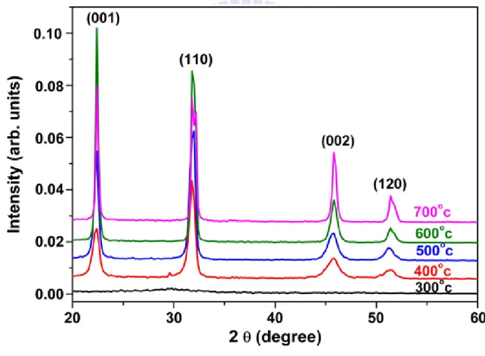
Figure 4.1 illustrates the results of conventional XRD ‘θ–2θ’ scan of BFO films deposited on the LNO-coated Si substrate at various temperatures. The film deposited at 300 °C exhibits a weak XRD pattern with broad lines, indicating a poorly crystallized film. At substrate temperature 700 °C, a randomly polycrystalline BFO film resulted, whereas a highly (001)-oriented BFO film was obtained for a substrate temperature in the range of 400 – 600 °C. The BFO (001) and (002) peaks are intense and narrow, indicating the satisfactory crystalline quality of BFO films deposited at 400 – 600 °C. To examine further the texture of the deposited films, we measured the width of the BFO (002) rocking curve (ω scan) as shown in the inset of Figure 4.1.1. The full width at half maximum (FWHM) of BFO (002) rapidly decreased to 3° for deposition temperatures of 400 – 600 °C. Such a narrow rocking curve clearly
demonstrates that the BFO films have a dominant <001> orientation. The narrower is the FWHM of this rocking curve, the better is known to be the crystalline quality.
Figure 4.1.1 XRD “θ–2θ” scan of BFO films deposited on a LNO-coated Si substrate at various temperatures. The inset shows the width of the BFO (002) rocking curve (ω scan).
To examine the in-plane structure of the BFO films, we measured in-plane grazing incidence X-ray diffraction as shown in Figure 4.1.2. The coexistence of (100), (200), (110) and (120) Bragg peaks in the in-plane radial scan along an arbitrary azimuth signifies that the in-plane structure is randomly oriented, as confirmed by the lack of intensity variation of the (110) Bragg peaks in an azimuthal scan (φ scan). The sputter-deposited BFO thin film has an extremely
c-oriented columnar textural structure. The XRD result shows that the BFO film
deposited at 500 °C has the best (001)-oriented crystal structure.
Figure 4.1.2 In-plane grazing-incidence XRD pattern of BFO films deposited on a Si substrate at various temperatures.
![Figure 2.3 Crystal structures of BiFeO 3 ;(A) tetragonal (B) unit cells [2].](https://thumb-ap.123doks.com/thumbv2/9libinfo/8747120.205183/29.892.135.796.476.990/figure-crystal-structures-bifeo-tetragonal-b-unit-cells.webp)
![Figure 3.7 Synchrotron Radiation [105].](https://thumb-ap.123doks.com/thumbv2/9libinfo/8747120.205183/47.892.150.796.117.879/figure-synchrotron-radiation.webp)
![Figure 3.8 Taiwan Light Source (TLS at NSRRC) [105].](https://thumb-ap.123doks.com/thumbv2/9libinfo/8747120.205183/48.892.261.679.113.1110/figure-taiwan-light-source-tls-nsrrc.webp)
![Figure 3.13 Schematic diagram of TF Analyzer 2000 [117].](https://thumb-ap.123doks.com/thumbv2/9libinfo/8747120.205183/59.892.146.796.113.797/figure-schematic-diagram-tf-analyzer.webp)