國立交通大學
電子物理系
碩士論文
飛秒雷射融蝕技術應用於硒化鋅奈米粒子之製作
The Fabrication of ZnSe Nanoparticles by Femtosecond Laser
Ablation Technique
研究生:王宣懿
指導教授:羅志偉 教授
飛秒雷射融蝕技術應用於硒化鋅奈米粒子之製作
The fabrication of ZnSe nanoparticles by femtosecond laser
ablation technique
研 究 生:王宣懿 Student:Hsuan-I Wang 指導教授:羅志偉 Advisor:Chih-Wei Luo 國 立 交 通 大 學 電 子 物 理 系 碩 士 論 文 A ThesisSubmitted to Department of Electrophysics College of Science
National Chiao Tung University in partial Fulfillment of the Requirements
for the Degree of Master
in Electrophysics
June 2010
Hsinchu, Taiwan, Republic of China
飛秒雷射融蝕技術應用於硒化鋅奈米粒子之製作 研究生:王宣懿 指導教授:羅志偉 博士 國立交通大學電子物理研究所 Abstract in Chinese 藉由飛秒雷射融蝕技術,具有六角晶系結構的硒化鋅奈米粒子可 以被輕易的製備出來。在本實驗中,不同雷射能量密度可製備特定粒 徑大小的奈米粒子,其大小可控制在 10 奈米~ 120 奈米,所注入的雷 射能量越大所得到的粒徑也較大。此外,值得注意的是飛秒雷射融蝕 技術所製備的硒化鋅粒子有結構相轉變的現象發生,也就是由原屬立 方晶系的結構轉成暫穩態六角晶系結構。其形成機制可以從熱力學的 觀點解釋,由於飛秒雷射瞬間注入能量誘發龐大的融蝕壓力致使硒化 鋅到達結構相轉變所需之壓力,才會由原本的穩定態結構變成暫穩態 結構。藉由本研究了解奈米結構的形成機制以及其性質將有助於我們 控制奈米結構的製作。
The fabrication of ZnSe nanoparticles by femtosecond laser
ablation technique
Student: Hsuan I Wang Advisor: Dr. Chih Wei Luo
Institute of Electrophysics National Chiao Tung University
Abstract in English
The free-standing hexagonal ZnSe nanoparticles have been successfully synthesized by femtosecond pulse laser ablation technique. We demonstrate the femtosecond laser ablation on a single crystal of ZnSe can be a simply useful method to form nanoparticles with tailored radii between ~ 10 nm to 120 nm by controlling the laser fluence. Furthermore, it is interesting to note that the fabricated ZnSe nanoparticles are metastable hexagonal phase. A picture of the growth mechanism of the metastable hexagonal phase ZnSe nanostructures will be proposed through thermodynamic point of view. Interesting, the structural phase transition is a photo-pressured triggered change from the metastable state to the stable state induced by the high peak power laser injection. It is important to note that the discussions of the nanostructure thermodynamics and stability can be applied to understand the growth mechanism of other nanostructures which are critical for optimization of the nanostructure.
Acknowledgement 能夠完成這篇關於飛秒雷射製作硒化鋅的研究其實並非我一人所及。 在研究的這條路上受到了許多人的幫助以及鼓勵,其中最重要的就是我的 父母無怨無悔的全力支持,讓我安心的在離家一百公里外專心做自己想做 的事情,也容忍我因為研究上的不順利而變得陰晴不定。 實驗室裡的大家也是我的精神支柱,雖然大家嘴巴上常常囔囔著要出 去散心、外面天氣風景多美好,卻從來沒看到大家願意放下手上的事情, 就算最後淪為嘴砲我也知道是因為大家都放不下屬於自己的責任,想要多 爭取一點時間好好完成研究,我想這就是讓大家能夠團結在這裡的原因 吧! 在研究道路上,過程必定是崎嶇的。感謝有 Kobayashi 老師、吳光雄 老師、Yabushita 老師、楊祝壽老師,以及我的指導教授羅志偉老師的細心 教導和支持,讓我不僅可以將自己的研究成果發表於各個會議,甚至還讓 我出國和各方交流,實屬寶貴難得的經驗,這是我一輩子都不會忘記的! 在最後,我還想感謝一路陪我走過的朋友們,因為有你們的陪伴我才 能堅持到這一步,即便是曾經有放棄的念頭也是因為你們的鼓勵才有今
Contents Abstract in Chinese ... i Abstract in English ... ii Acknowledgement...iii Contents ... iv Figure Caption ... vi Table Caption ... ix
Chapter 1: Introduction and Motivation ... 1
1.1 General Introduction of Nanometer Materials... 1
1.2 Nanoparticle Fabrication Methods... 3
1.2.1 Laser Ablation Method ... 5
1.2.2 Vapor Synthesis Method... 6
1.2.3 Chemical Reduction Method... 7
1.3 Applications of Semiconductor Nanoparticles ... 8
1.4 Motivation ... 10
Chapter 2: Interaction between Femtosecond Laser and Materials ... 11
2.1 The Main Excited Process in Materials ... 13
2.2 Linear Absorption ... 15
2.3 Nonlinear Absorption... 16
Chapter 3: Experiments and Techniques... 19
3.1 Experimental Framework... 19
3.2 ZnSe Nanoparticles Fabrication... 20
3.2.1 The Experimental Setup ... 20
3.2.2 ZnSe Nanoparticles Preparation ... 22
3.3 Characterization Technique... 23
3.3.1 Laser Pulse Duration Control ... 23
3.3.2 Energy Dispersive X-ray Analysis (EDX) ... 27
3.3.3 X-ray Diffraction (XRD) ... 28
3.3.4 Transmittance Electron Microscope (TEM)... 30
3.3.5 Knife Edge Measurement ... 32
Chapter 4: Results and Discussion... 35
4.1 The Fabrication Conditions of ZnSe Nanoparticles ... 35
4.2 The Formation of ZnSe Nanoparticles... 37
4.3 The Composition of ZnSe Nanoparticles... 41
4.4 The Crystalline Structure of ZnSe Nanoparticles ... 42
4.5 The TEM Images of ZnSe Nanoparticles ... 51
4.6 The Size of Nanoparticles ... 53
Chapter 5: Summary... 56
Figure Caption
Figure 1.1: Density of states in one band of a semiconductor as a function of dimension [7]. ... 2 Figure 1.2: The schematic diagram of silver nanoparticles formation by laser
ablation [8]. ... 5 Figure 1.3: Electron micrographs and size distributions of the gold nanoparticles
produced by 1064-nm laser ablation at 80 mJ/pulse [9]... 5 Figure 1.4: Counterflow jet technique used for vapor-phase synthesis of ZnSe
nanoparticles [11]... 6 Figure 1.5: Transmission electron micrograph shows the polycrystalline
structure of a composite ZnSe nanoparticle [11]. ... 6 Figure 1.6: TEM micrograph and size distribution of nickel nanoparticles made
through hydrazine reduction in ethylene glycol [13]... 7 Figure 1.7: Density of sate in semiconductor bulk and nanocrystals... 8 Figure 1.8: Emission color under UV illumination for colloidal CdSe/ZnS QDs
with various sizes [14]. ... 9 Figure 2.1: The schematic of electron and lattice excitation and relaxation
processes in a laser-excited direct gap semiconductor [17]... 14 Figure 2.2: The schematic of linear absorption and nonlinear absorption [20]. . 15 Figure 2.3: The diagram of Gaussian beam and processed region near focus
point. ... 18 Figure 3.1: The experimental setup diagram of femtosecond laser ablation
system... 21 Figure 3.2: Basic principle of second-order autocorrelation: noncolinear
Figure 3.3: The inner part of the laser amplifier. The labeled component is the
chirp controller. ... 24
Figure 3.4: The pulse width results by autocorrelator measurement at different chirp. ... 25
Figure 3.5: The pulse width varying as the chirp controller away from the zero point. ... 25
Figure 3.6: The scheme of experimental setup for pulse width inspection... 26
Figure 3.7: The pulse duration at the highest intensity white light. ... 26
Figure 3.8: The schematic diagram of EDX... 27
Figure 3.9: (a) Experimental setup of x-ray diffraction and (b) the diagram of its basic concept. ... 28
Figure 3.10: The diagram of the transmission electron microscopy [27]. ... 31
Figure 3.11: In fact, there is diffraction around the barrier as shown with some exaggeration... 32
Figure 3.12: The simulation of knife edge measurement signal. ... 34
Figure 4.1: The experimental setup in lab... 35
Figure 4.2: The ZnSe nanoparticles preserved in the alcohol. ... 36
Figure 4.3: The ZnSe wafer before and after the femtosecond laser ablation. ... 37
Figure 4.4: The reflectivity of ZnSe wafer as a function of laser fluence. ... 38
Figure 4.5: The spectrum of femtosecond laser pulses irradiated on the ZnSe single crystals... 40
Figure 4.6: EDX analysis shows the composition of ZnSe nanoparticles. ... 41
Figure 4.7: The X-ray diffraction pattern of ZnSe wafers. ... 42
Figure 4.8: The X-ray diffraction pattern of ZnSe nanoparticles... 42 Figure 4.9: The XRD patterns of ZnSe nanoparticles under various laser
Figure 4.10: The XRD patterns of ZnSe nanoparticles under various laser
fluences. ... 44 Figure 4.11: The (a) cubic and (b) hexagonal structures of ZnSe... 45 Figure 4.12: Part of phase diagram for ZnSe [33]... 46 Figure 4.13: The simulated ablation pressure as a function of power density. 49 Figure 4.14: Resistance as a function of pressure in ZnSe [44]... 50 Figure 4.15: (a) TEM image of ZnSe nanoparticles at F= 144 mJ/cm2... 51 Figure 4.16: (a) TEM image of ZnSe nanoparticles at F= 205 mJ/cm2... 52 Figure 4.17: (a) TEM image of ZnSe nanoparticles at F= 127 mJ/cm2. (b)The
electron diffraction pattern of the ZnSe nanoparticles in (a)... 52 Figure 4.18: The peak fitting with the Gaussian function in the X-ray diffraction
pattern... 53 Figure 4.19: The size of ZnSe nanoparticles as a function of various laser
Table Caption
Table 1. Methods of nanoparticles fabrication ... 4 Table 2. various lasers and its application... 12 Table 3. The comparison between femtosecond laser and conventional laser.... 17 Table 4. The fabrication condition of ZnSe nanoparticles. ... 36 Table 5. The size of ZnSe nanoparticles under various laser fluences... 54
Chapter 1: Introduction and Motivation
1.1 General Introduction of Nanometer Materials
“There’s plenty of room at the bottom, that…almost any chemically stable structure, that can be specified, can in fact be built….”
Richard P. Feynamn [1]
Over last decades, a completely new field with small size was rapidly developed and intensively investigated since the bulk materials have been widely explored and well understood. In 1959, a speech to the American Physical Society given by a famous physicist, Richard P. Feynamn, had mentioned the concept of the material in much smaller scale, for instance in nanometer scale. Recently, the materials in nanometer have an astonishing progress and scale and the nanometer sized material has attracted much attention because of its distinct physical properties. With decreasing the size, the atoms located on the surface of nanomaterials become dominant. Due to the unique dimension dependent properties and the potential applications such as building blocks in nanoelectronics, nanosensors, nano-optronics and chemical catalyst [2-6], the nanostructures and their assembly are of fundamental importance. The researches of nanometer crystallites provide an opportunity to observe the evolution of material properties with size, such as quantum confinement effect, surface area effect, volume effect, tunneling effect and size effect. In the optical properties point of view, the reflection of nanocrystals is worse than the bulk material because of the particle size is much smaller than the wavelength of UV-light.
important role on determining the electronic and optical properties. According to the confined dimensions of excited electrons and holes, the nanometer-sized material can be divided into three parts, the quantum well for one dimension, nanowires for two dimensions and nanoparticles for all three dimensions.
The materials in different confinements are corresponding to its unique density of state (Figure 1.1).
Density of states
0D 1D
2D 3D
Figure 1.1: Density of states in one band of a semiconductor as a function of dimension [7].
Energy
In nanoparticles case, it shows a large fraction of surface atom per unit volume. Because of the vast surface area, all nanoparticles have a huge surface energy and, thus often form aggregation as a result of attractive van der Waals force to minimize the total surface energy and its density of state is between the atoms and bulk materials. The energy level of nanoparticles is similar to the atoms and the molecules. The density of states increases while the nanoparticles size decreases. As the results, the electronic, optical, and magnetic properties will be affected through altering the size nanoparticles.
1.2 Nanoparticle Fabrication Methods
In general, the methods of nano-material fabrication can be divided into two categories.
The top-down approach indicates the technique where the extent and dimensionality of solid matter gradually reduced by using lithography patterning, mechanical milling, photo mask, etc. The bottom-up method utilizes the growth and self-assembly to build nanostructures from atomic or molecular precursors which includes the thermal evaporation, liquid phase chemical precipitation, hydrothermal, epitaxy growth and chemical vapor deposition.
Generally, it is usually difficult to obtain the structures which are smaller than 50 nm through top-down approached, while the bottom-up method is typically hard to gain structures larger than 50 nm. When the extent of a solid is reduced in one or more dimensions, the physical, magnetic, electrical, and optical properties can be dramatically changed. The size distribution and particle type can be determined in the nanoparticles fabrication through controlling the growth conditions and then the core-shell structured nanoparticles might be achieved. Both approaches have merits and disadvantages; it depends on the requirements and the specific applications for nanoparticles. Table 1 shows some methods on nanoparticles fabrication. Additionally, following three kinds of main process on nanoparticles fabrication will be briefly introduced.
Table 1: Methods of nanoparticles fabrication
Physical Methods Chemical methods
Laser ablation Chemical vapor deposition (CVD) Physical vapor deposition (PVD) Sol-gel method
Mechanical alloy (MA) Self expansion synthesis (SHS) Thermal evaporation Hydrothermal
Spray conversion process
Sonochemical method
Complex pyrogenation
Reverse micelle synthesis
Solvothemal method
1.2.1 Laser Ablation Method
The main idea of laser ablation is performed through the high energy laser which ablates the bulk materials into the size of nanometer scale. The experiments of laser ablation on metallic nanoparticles production presented here were developed by Professor Kondow group [8]. In this research, they demonstrated that silver nanoparticles were produced by laser ablation of a metal silver plate in an aqueous solution of sodium dodecyl sulfate, C12H25OSO3Na. For laser ablation technique, usually a
specific aqueous solution is required to prevent the nanoparticles from assembly. The same experimental concept is also applied to the formation of gold nanoparticles [9].
Figure 1.2: The schematic diagram of silver nanoparticles formation by laser ablation [8].
Figure 1.3: Electron micrographs and size distributions of the gold nanoparticles produced by 1064-nm laser ablation at 80 mJ/pulse [9].
1.2.2 Vapor Synthesis Method
For vapor synthesis method, the vaporized materials assemble into nanoparticles through the cooling and aggregation. In order to prepare the solid material in nanoparticulate form, the mixed vapor phase will be controlled in the conditions of relatively unstable thermodynamics. Once the particles form in the gas phase, they coagulate with a rate which is proportional to the square of their concentration and weakly dependends on the particle size. Hahn [10] presented a useful overview of the gas-phase synthesis for nanocrystalline materials. Figure 1.4 and Figure 1.5 shows the results of ZnSe nanoparticles produced by Sarigiannis’s group through vapor synthesis method [11].
Figure 1.4: Counterflow jet technique used for vapor-phase synthesis of ZnSe nanoparticles [11].
Figure 1.5: Transmission electron micrograph shows the polycrystalline structure of a composite ZnSe nanoparticle [11].
1.2.3 Chemical Reduction Method
The coprecipitate process occurs when specific chemical solution mixed together to produce desired nanoparticles. By controlling the experimental conditions, the particle size can be determined. Che’s group has demonstrated the preparation f ZnSe nanometer powder by reduction process [12].They represent the reaction as follows:
Zn(Ac)2 + H2SeO4 → ZnSeO4 + 2HAc
ZnSeO4 + 4CO → ZnSe + 4CO2
From their experiment results, the lowest temperature for the formation of single-phase ZnSe nanocrystals is 460 ℃ and the average diameter of the
crystallited powder at 460 ℃ is around 25 nm.
The nickel nanoparticles also can be obtained through the similar process. In 2003, S.-H. Wu and D.-H. Che synthesized the nickel nanoparticles by the hydrazine reduction of nickel chloride in ethylene glycol at 60 ℃ without soluble polymer.
2Ni2+ + N2H4 + 4OH-→2Ni+ N2 + 4H2O
Figure 1.6: TEM micrograph and size distribution of nickel nanoparticles made through hydrazine reduction in ethylene glycol [13]
1.3 Applications of Semiconductor Nanoparticles
Over the last decade, the studie of nanoparticles on semiconductor materials have developed rapidly. Semiconductor nanocrystals exhibit a wide range of size-dependent properties. Variations in the fundamental characteristics, e.g. the phase transitions, electrical conductivity, etc., can be carried out by controlling the size of the crystals. In this section, we review the present status and new opportunities for researches in the field of materials physical chemistry. For semiconductors in thenanometer scale, the electronic states become partially discrete as in atoms and molecules besides the widening of band gap appears.
Figure 1.7: Density of sate in semiconductor bulk and nanocrystals. In each case, the density of states is discrete at the band edges. The Fermi level is in the center of a band in a metal, and so kT will exceed the level spacing even at low temperature and small sizes. The gap increases in semiconductor nanocrystals with smaller size [7].
Due to its special physical properties, the semiconductor nanoparticles have been employed to modify the conventional electronic-photonics device.
For instance, the light emitting diode (LED) can irradiate the light in different wavelength without changing the material of active layer but utilizing the same substance in various sizes. The CdSe/ZnS quantumdots can illuminate different color has been well investigated [14].
Figure 1.8: Emission color under UV illumination for colloidal CdSe/ZnS QDs with various sizes [14].
The semiconductor nanocrystals are also applied on the biological labels [7, 15]. In traditional, the biological label was made of organic dyes which might induce huge damage. On the contrary, the semiconductor nanoparticles are quite stable and safe. And by the effective surface modification and controlled particle size, the proteins and DNA can be labeled by different nanoparticles with different colors.
1.4 Motivation
As the rapid development of micro electro-mechanical system, the requirements on well quality and small-sized device become the main issue in technology. How can we fabricate a high quality nanostructure or nanocrystal with a fast, easy and convenient approach? A new technique called femtosecond laser ablation might be taken into consideration.
The femtosecond laser ablation technique has been widely applied, such as the laser annealing, micromachining and device defect restoration. Due to its sufficiently high energy density, the advantages of utilizing femtosecond laser as a tool includes less heat affected zone, only destroy the unfavorable region and no limitations on the processed material including the material whose band gap is larger than the laser photon energy. There are various methods on nanoparticles fabrication, such as vapor synthesis, Spray conversion process and etc. But none of them provides an all-purpose way to obtain nanoparticles. Here we offer a new way to produce nanoparticles with the femtosecond laser ablation technique.
ZnSe is a direct band gap semiconductor, with a band gap energy and an emission at 2.7 eV, which suggests that ZnSe is applicable for photoelectronic devices. ZnSe also has potential application in optically controlled switching due to its giant photoresistivity. As a result, we choose ZnSe as the processing material and try to figure out the characteristics of ZnSe nanoparticles made by femtosecond laser ablation.
Chapter 2: Interaction between Femtosecond Laser and Materials
Up to now, many kinds of lasers have been developed well, which could be generally classified to two sorts, i.e. the pulse lasers and the continuous wave lasers. Various wavelengths and power can be provided by choosing different gain medium and cavity components. The detailed classification is shown in Table 2 [16].
Recently, the rapid development of the researches on femtosecond laser has attracted extensive attention, especially the applications in material science, medicine, and industry due to its drastically difference from the conventional pulsed laser, while the materials are irradiated by the femtosecond laser, the mainly physical effect is the laser ablation or material removal which can be used in thin film deposition, material cleaning, picture restoration, new material creation, and micro-machining.
The femtosecond laser ablation has been extensively shown in both absorptive and transparent materials. For these two different materials, they undergo a quite unfamiliar way with femtosecond laser. We can classify the interaction between femtosecond laser and the materials into two regimes. First, thermalization takes place when the laser pulse width is longer than the electron-lattice scattering time and thermal diffusion time corresponding to the skin depth. Second, if the intensity of a femtosecond laser pulse is high enough, the highly nonlinear absorption process will occur in materials without absorbing the fundamental wavelength.
Table 2. Various lasers and its application [16].
Sort Conventional laser Ultrafast laser
Medium type
Gas Liquid Solid Solid
Laser He-Ne laser Argon Laser CO2 Laser Excimer Laser Dye Laser
Semiconductor Laser
Nd:YAG Laser Ti: Sapphire Laser
Yb Laser
Medium Ne Ar CO2
ArF, KrF.
XeCl, XeF Rhodamine 6G
GaAlAs/GaAs, nGaAsP/InP,
(PbSn)SnTe
Nd:YAG Ti: Sapphire Yb
Output C.W. C.W. C.W. Long pulse Long pulse, C.W. Long pulse, C.W. Short pulse Short pulse Short pulse
Wavelength 632.8 nm 488 nm, 514.5 nm 10.6 µm 193 nm, 248 nm, 308 nm, 351 nm 532 nm ~ 610 nm 0.39 µm ~ 15 µm 1.054 µm, 1.064 µm 750 nm ~ 850 nm 1.035 µm, 1.053 µm Max. output power Low (~ 50 mW) Low (~ 200 mW) High (> 1000 W) High (> 50 W) Mid.(< 10 W) < 2 W < 20 W < 5W < 1W Application Printer, Spectroscopy, Cell fluorescence, Manufacture, Radard, Precise manufacture,
Spectroscopy Memory, Radard Communication, Precise
Communication, Precise
2.1 The Main Excited Process in Materials
The interaction between the femtosecond laser pulses and materials dramatically differs from that between the long pulses (or continuous wave light) and materials.
First, the energy delivery occurs in a short enough timescale compared to any relaxation processes. The laser energy is absorbed by the electrons, leaving the ions cold. After the laser pulse is gone the thermalization takes place. Second, the intensity of a femtosecond pulse, even with very moderate energy, is high enough to drive highly nonlinear absorption processes in materials that normally do not absorb at the laser wavelength.
After excitation by an ultrashort pulse, a semiconductor undergoes several relaxation processes. The laser deposited energy is transferred to the electrons and than the lattice. The interaction includes various regimes of carrier excitation and relaxation which can be roughly distinguished into four types: (1) carrier excitation, (2) thermalization, (3) carrierremoval, (4) thermal and structural effects [23]. In Figure 2, the several processes do not show sequentially, but overlap in time and form a continuous chain events spanning the entire range from femtoseconds to microseconds. The mechanisms of electron and lattice dynamics for these four types are complicated.
(1) When the photon energy is larger than the bandgap, single photon absorption is the dominant mechanism for exciting the electrons from valence band to conduction band.
(2) The electrons and holes are redistributed throughout the conduction and valence band by carrier-carrier and carrier-phonon scattering.
(3) As the carriers and the lattice are in thermal equilibrium, the material is at a defined temperature. There still is an excess of free carriers compared to it in thermal equilibrium although the carrier distribution has the same temperature. The excess carriers are removed either by recombination of electrons and holes or by diffusion out of the excitation region.
(4) The material excited by femtosecond pulse laser can achieve thermal equilibrium situation just few picoseconds. But it takes longer time to remove the excess carriers. Once the lattice temperature exceeds the melting point or the boiling point, the vaporization or melting can occur.
Figure 2.1: The schematic of electron and lattice excitation and relaxation processes in a laser-excited direct gap semiconductor [17]. (a) Multiphoton absorption. (b) Free-carrier absorption. (c) Impact ionization. (d) Carrier distribution before scattering. (e) Carrier-carrier scattering. (f) Carrier-phonon scattering. (g) Radiative recombination. (h) Auger recombination. (i) Diffusion of excited carrier. (j) Thermal
2.2 Linear Absorption
For non-metallic materials, the highest energy level occupied by an electron is partitioned by an energy gap from the lowest energy level that is unoccupied. If the photon energy exceed the bandgap energy, light can be absorbed by the materials and exciting electrons from valence band to conduction band [18]. For metals, the conduction band is partially occupied, providing unoccupied energy levels at slightly higher energy than occupied ones. If the light irradiates on this material, photons can be absorbed through free-carrier absorption. The free carrier gains energy by absorbing a photon and gains momentum through an interaction with a phonon, also called lattice vibration, to move to a higher level in conduction band [19]. Under this condition, material ablation can occur if sufficient laser energy is deposited into surface.
Figure 2.2: The schematic of linear absorption (left) and nonlinear absorption (right) [20].
2.3 Nonlinear Absorption
In the case of the materials which are transparent at laser wavelength, a single photon of light does not have enough energy to excite an electron from valence band to conduction band. The only way for performing absorption at fundamental laser wavelength is through the nonlinear process. The basic requirement for occurring nonlinear absorption is enough energy density deposited into the materials. Because the absorption is nonlinear, i.e. the absorption probability is a nonlinear function of the laser intensity, the absorption can be performed inside a transparent sample by tightly focusing the laser beam inside the sample which provides a much higher laser intensity in the focal volume than that at the surface. There are two kinds of nonlinear excitation mechanisms, i.e. photoionization and avalanche ionization, that play a role in this type of absorption [21].
In photoionization case, the electrons are directly excited from the valence to the conduction band by the laser. Depending on the laser frequency and intensity, there are two different regimes of photoionization, i.e. the multiphoton ionization regime and the tunneling ionization regime, which were shown to be two limits in the same process by Keldysh [22].
For the avalanche ionization, it involves free carrier absorption and followed by impact ionization. An electron in the conduction band sequentially absorbs several photons until its energy exceeds the conduction band maximum by more than the bandgap energy, and then collisionally ionizes another electron to leave two electrons at the conduction band minimum [21, 23]. As long as this process occurred by the laser field repeatly, the electron density in the conduction band grows
2.4 The Advantages for Using Femtosecond Laser
Comparing to the conventional laser processes, the energy in femtosecond laser case is delivered in an ultrashort time scale (~100 fs). Because a single pulse processing time on the materials is smaller than the heat diffusion time, which will increase the efficiency of the absorption of laser energy [24, 25]. As a result, using femtosecond laser as the material processing light source can obtain less damage, less residual strain force and less structure transformation.
Following Table shows the comparison between the conventional laser process and the femtosecond laser process.
Table 3. The comparison between femtosecond laser and conventional laser [26]. Laser Femtosecond Laser Conventional Laser Output Type Short pulse Continuous wave, long pulse Mechanism Ionization (cold process) Vaporization (hot process)
Scale Subnanometer Few micrometer
Advantage
1. small scale machining 2. No thermal influence 3. No material limitation 4. high energy utility 5. occur only at focal point
1.fast process
2. application of welding
Disadvantage
1.small processed area 2. slow processing speed 3. laser alignment
1. thermal diffusion
2. influence the structure near the processed area
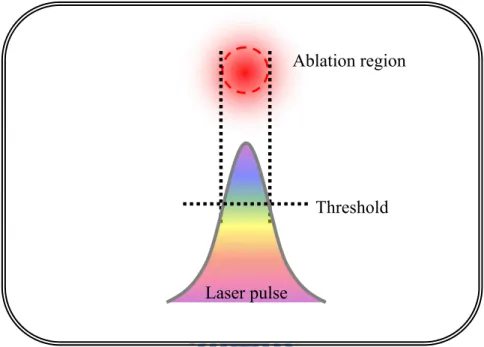
Besides, the spatial distribution of the energy of femtosecond laser is Gaussian distribution as shown in Figure 2.3. The density is higher as closing to the center of laser beam and vice versa. Due to this energy distribution, the microstructure which is smaller than the focused spot size can be achieved by adjusting proper energy parameters over the threshold of materials.
Figure 2.3: The diagram of Gaussian beam and processed region near focus point. Laser pulse
Ablation region
Chapter 3: Experiments and Techniques 3.1 Experimental Framework Transmission Electronic Microscopy X-ray Diffraction Energy Dispersive Spectrometer Composition Inspection Structure Identification Other Characteristics Size of Nanoparticles The ZnSe nanoparticles fabrication by
3.2 ZnSe Nanoparticles Fabrication 3.2.1 The Experimental Setup
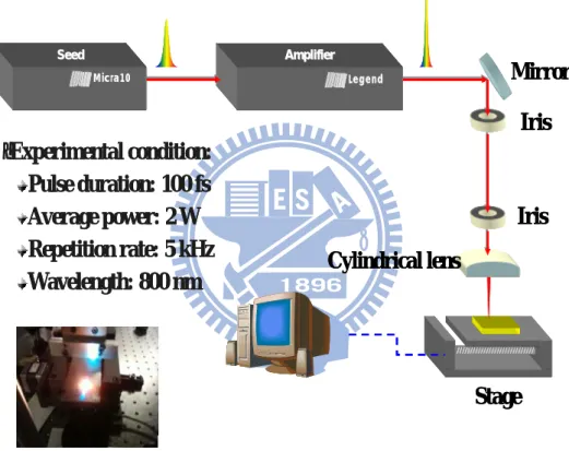
In this experiment, the laser source plays an important role to cause certain process happened in the materials. In order to reach the nonlinear absorption region, the high pulse energy light source is required. The low-energy 100-fs pulses at 800 nm were produced by a mode-locked Coherent Micra10 Ti:sapphire laser pumped by a Coherent Verdi diode pump solid state laser. After stretching to ~ 200 ps, pulses were synchronously injected into a Ti:sapphire regenerative amplifier (Coherent Legend series) pumped by a 1-kHz Nd:YLF laser and the amplified pulses (~12 mJ) were recompressed to τp ~ 30 fs with pulse energy ~ 0.4 mJ.
All experiments were carried out at 1 kHz repetition rate. For preliminary ablation studies on zinc selenide, the substrate was scanned under the focused laser spot with motorized X-Y-Z translation stages. Pulse energy was varied by a metallic neutral density filter with OD 0.1-2 (Thorlabs ND series). A 100 mm focal length plano-convex fused silica cylindrical lens was used to focus the output of the femtosecond laser into a line-spot on the surface of the samples as shown in Figure 3.1. For micromachining of ZnSe at 800 nm aimed at nanoparticles fabrication, a high resolution scanning stage is required with the scanning speed varying from 10 µm/sec to 120 µm/sec.
Legend Legend Micra10Micra10 Amplifier Amplifier Seed Seed •Experimental condition: Pulse duration: 100 fs Average power: 2 W Repetition rate: 5 kHz Wavelength: 800 nm Iris Iris Cylindrical lens Mirror Stage Legend Legend Micra10Micra10 Amplifier Amplifier Seed Seed Legend Legend Legend Legend Legend Legend Micra10Micra10 Micra10Micra10 Micra10Micra10 Amplifier Amplifier Seed Seed •Experimental condition: Pulse duration: 100 fs Average power: 2 W Repetition rate: 5 kHz Wavelength: 800 nm Iris Iris Cylindrical lens Mirror Stage
3.2.2 ZnSe Nanoparticles Preparation Experimental procedure:
(1) A single-side polished ZnSe chip with cubic structure was used as the initial materials of nanoparticles fabrication.
(2) To clean the ZnSe chip surface, the 95% alcohol with paper was applied.
(3) The ZnSe wafer was cut into several pieces with the size f 5 mm×5 mm by tungsten steel pen.
(4) The laser spot size was characterized by the knife edge measurement and the laser fluence was defined by the following formula
(
)
size Spot rate repetition power Laser F Fluence= = / (Eq. 3.1)(5) The ZnSe sample prepared by step (3), which was placed on a motorized translation stage with the speed of 40 µm/sec, was scanned with femtosecond pulse laser.
(6) For the purpose of size measurements and TEM observation, ZnSe nanoparticles were well preserved in concentration 95% ethanol. (7) Some of the ZnSe nanoparticles were attached by the tape for the
3.3 Characterization Technique 3.3.1 Laser Pulse Duration Control
For laser ablation technique, the laser pulse width plays an important role to decide which procedure it takes melting, vaporization or ionization. The laser pulse width should be fixed in certain range, especially for those cases in which the material only can absorb the laser photon energy through multiphoton absorption.
The information of laser pulse width can be obtained through an autocorrelator (Figure 3.2).
Figure 3.2: Basic principle of second-order autocorrelation: noncolinear arrangenent. Lens Retro-reflector Mirror Nonlinear crystal Photodetector 2nd harmonic Input pulse Beam splitter △t
In the laser amplifier system, a chirp controller was equipped to modify the output laser pulse as shown in Figure 3.3. By adjusting this component, system will provide negative or positive chirp to modify pulse duration.
Figure 3.3: The inner part of the laser amplifier. The labeled component is the chirp controller.
Following figure (Figure 3.4, Figure 3.5) shows the results that pulse shape and pulse width at different chirp. At 0 step, the pulse shape was much Gaussian-like pulse and symmetric, the pulse width is about 80 fs. Once we moved the chirp controller away from the zero step, the pulse shape began to distortion and the pulse width became much broaden as increasing the distance from zero point. Therefore, the chirp should be precisely controlled to maintain better processing quality.
-1.0 -0.8 -0.6 -0.4 -0.2 0.0 0.2 0.4 0.6 0.8 1.0 A m plitude (a .u.) Delay Time (ps) -30 -25 -20 -15 -10 -5 0 +5 +10 +15 +20 +25 +30
Figure 3.4: The pulse width results by autocorrelator measurement at different chirp.
-30 -20 -10 0 10 20 30 50 100 150 200 250 300 350 400 P u lse w id th (f s)
Distance of chirp controller (step)
pulse width (fs)
Figure 3.5: The pulse width varying as the chirp controller away from the zero point.
Here we provide a convenient approach to confirm the laser pulse is at the smallest pulse duration, or the highest peak power. A convex lens and a sapphire chip (~5 mm in thickness) are required, the setup is shown in Figure 3.6.
Figure 3.6: The scheme of experimental setup for pulse width inspection. Pulse Laser
Sapphire chip Screen Convex lens
Because of self-phase-modulation phenomena, it indicates a nonlinear optical effect of light-matter interaction which will induce the variation in refractive index and will produce a phase shift in the pulse, leading to a change of the pulse's frequency spectrum. In our case, when high power density laser irradiated on a sapphire chip will trigger the white light production. By modifying decent chirp to the shorter pulse duration, we can obtain the broadest spectrum and highest intensity white light. Through the measurement on the pulse width, we found that when the triggered white light is at the highest intensity the pulse duration is ~81 fs corresponding to the pulse duration at zero step in Figure 3.4. As the result, we can utilize this simple method to check the processing laser pulse width.
-1.0 -0.8 -0.6 -0.4 -0.2 0.0 0.2 0.4 0.6 0.8 1.0
Pulse duration at highest intensity white light
A m plit ude ( a .u .) Time (ps)
3.3.2 Energy Dispersive X-ray Analysis (EDX)
X-ray detector
Figure 3.8: The schematic diagram of EDX.
The energy dispersive X-ray Analysis is an analytical instrument for the element analysis and chemical characterization which is usually equipped with SEM. The main idea is to investigate the x-ray fluorescence induced by the interactions between electromagnetic radiation and matters. The emitted x-ray is response to the matter being hit with charged particles and its energy depends on the materials under examination. The X-rays are generated in a region about 2 microns in depth, thus EDX is not a surface science technique. Because each element has its unique atomic structure, the x-rays are allowed to identify one element from another element.
The SiLi detector is often protected by a Beryllium window. Elements with low atomic number are difficult to detect via EDX. The soft X-rays absorption of Be will limit the detection of elements below an atomic number of 11 (Na). In windowless systems, elements with as low atomic number as 4 (Be) have been detected, but the problems involved get progressively worse as the atomic number is reduced.
Electron beam
Amplifier Si(Li)
detector
Liquid nitrogen Dewar
3.3.3 X-ray Diffraction (XRD)
The information of the sample structures and orientation can be obtained through x-ray diffraction patterns which were taken from a Bruker X-ray diffraction D2 PHASER using Cu Kα radiation from a rotating anode x-ray generator and operating at 10 kV / 30 mA. The angle between the sample holder and incident x-ray was θ and the detector has a 2θ rotation as θ changes. Figure 3.9 shows the experimental setup of x-ray diffraction and the diagram of its basic concept.
(a) (b)
Figure 3.9: (a) Experimental setup of x-ray diffraction and (b) the diagram of its basic concept. 2θ 2θ readout Detector θ readout Specimen X-ray tube θ θ Diffracted Beam Incident Beam d hkl θ
The scattering occurred when the incident beam irradiating on the sample. X-rays scattered from adjacent planes will lead to constructive interference when the angle θ between the plane and the x-ray results in a path-length difference that is an integer multiple n of the x-ray wavelength λ. This is Bragg’s law and can be expressed as:
λ
θ
n d sin =2 (Eq. 3.2)
Here d is the spacing between diffracting plane, θ is the angle between the incident light and sample surface, λ is the wavelength of incident beam, n is any integer.
The X-ray diffraction patterns show the relation between θ and interference intensity. The orientation of each peak can be identified through consulting the ICDD-JCPDS (International Centre for Diffraction Data of Joint Committee on Powder Diffraction Standards).
3.3.4 Transmittance Electron Microscope (TEM)
The transmission electron microscopy is one of the instruments to observe the materials in microscopic scale which carries out the information of morphology and crystallography. The TEM can provide significantly higher resolution than the optical microscopy such as the arrangement of atoms in the specimen and their degree of order, detection of atom-scale defects in areas a few nanometers in diameter because of the smaller de Broglie wavelength of electrons.
The TEM operation is similar to the projector, which irradiate the light through the slide and the light is affected by the objects on the slide. With the same idea, the TEM replaces the light source with an electron gun in which a thin specimen illuminated with electrons. The images formation of TEM is by utilizing the massage contained in the electron waves exiting from the samples.
Another characteristic is the crystalline of a specific region, the structure can be identified through selected area diffraction. The diffraction patterns come from the interaction between the electron beam and specimen. Here the electron beam is considered as a wave-like, rather than particle-like and the sample structure is treated as the diffraction grating to electrons. Therefore, the image on the screen of the TEM will be a series of dots, the selected area diffraction pattern, and each dot corresponding to a satisfied diffraction condition of the sample's crystal structure.
3.3.5 Knife Edge Measurement
During laser processing, the energy density (laser fluence) is an important parameter. It dominants what kind of mechanism takes place such as vaporization, ionization, and melting. There are two variable parameters, i.e. laser power and spot size, included in energy. Spot size can be determined through various methods, e.g. knife edge measurements and laser beam profiler. In this thesis, the knife edge measurement is applied to decide the laser beam size. It is explained by Huygens-Fresnal principle. As shown in Figure 3.11, the barrier plays a role to block the propagation of the electromagnetic wave which acts as a secondary source and create a new wave front [28].
Figure 3.11: In fact, there is diffraction around the barrier as shown with some exaggeration. Propagation
Barrier
Generally, the distribution of laser power is Gaussian. The electric field can be expressed as Eq. 3.3. The laser intensity and power are proportional to square of electric field Eq. 3.4, here w is the spot size.
) ( ) ( 2 2 2 1 2 ) ( w i t k r y x e e w r E − ⋅ + − = ω π (Eq. 3.3) 2 2 2 ) ( 2 2 2 2 w y x e w E I P + − ∝ ∝ ∝
π
(Eq. 3.4)The distribution at x-axis can be obtained by integrating the y (Eq. 3.5) and simplified by Error function, Erf[x] (Eq. 3.6). By integrating the Eq. 3.5, the function of power distribution to x-axis can be obtained and shown as Eq. 3.6.
] 2 [ 2 1 1 2 2(2 ) 2 2 2 2 2 2 a Erf e dy e w x a a y x − − + − =
∫
π
π
(Eq. 3.5)∫
−=
x tdt
e
x
Erf
0 22
]
[
π
(Eq. 3.6) ]) 2 [ ] 2 [ ]( 2 [ 2 1 ] 2 [ 2 1 22 a Erf a Erf a Erf dx e a Erf x a x + =∫
− −π
(Eq. 3.7)The laser spot size is calculated with the inverse concept. The signal measured from knife edge measurement is in the similar form of Eq. 3.7. The first step of data processing is to differentiate the measured signal. Following procedure is fitting the differential data with Gaussian curve. And the spot size in this study is defined by the full width at half maximum of Gaussian distribution. Following figure presents the simulation signals of knife edge measurement.
Differentiation -4 -2 0 2 4 0.0 0.1 0.2 0.3 0.4 Intensi ty (a.u .) r (a.u.) Move distance (a.u.)
L a se r p o w er (a .u .) -4 -2 0 2 4 0.0 0.2 0.4 0.6 0.8 1.0
Chapter 4: Results and Discussion
4.1 The Fabrication Conditions of ZnSe Nanoparticles
In this experiment, all the ZnSe nanoparticles are fabricated under ambient condition and various laser fluences which are varied by using the neutral density filter. The spot size of processing laser was determined by knife-edge measurements.
All of the ZnSe nanoparticles were obtained under the following condition: [ Environment temperature: 24 ℃
[ Environment humidity: 42 % [ Environment pressure: 760 torr [ Laser spot size: 66 µm × 1691μm
Figure 4.2: The ZnSe nanoparticles preserved in the alcohol.
Table 4. The fabrication condition of ZnSe nanoparticles. Sample number Fluence (mJ/cm2) Sample number Fluence (mJ/cm2) ZnSe-01 25 ZnSe-10 185 ZnSe-02 34 ZnSe-11 198 ZnSe-03 42 ZnSe-12 220 ZnSe-04 44 ZnSe-13 235 ZnSe-05 51 ZnSe-14 249 ZnSe-06 109 ZnSe-15 264 ZnSe-07 135 ZnSe-16 304 ZnSe-08 156 ZnSe-17 340 ZnSe-09 172 ZnSe-18 400
4.2 The Formation of ZnSe Nanoparticles
After laser ablation, a large amount of ZnSe nanoparticles were found on the laser ablated wafer as shown in Figure 4.3.
Before laser process After laser process
Figure 4.3: The ZnSe wafer before and after the femtosecond laser ablation.
In 2006, Jia’s group reported the formation of the nanowires on the ZnSe wafer induced by femtosecond laser in water [30] and in air [31]. They claimed that this kind of reactions is a self-catalyzed process. For our experiments, the formation of the ZnSe nanoparticles on the wafer surface also can be comprehended by similar concept. As the laser ablation takes place on the wafer in air, unlike those in vacuum chamber, the ablation plume was confined around the laser focal point by the atmosphere and induced an instantaneously high energy density and high pressure at laser focus point. A large amount of the ZnSe nanoparticles in the plume adhered on the sample surface. As a result, the ZnSe nanoparticles grow very rapidly.
Besides, during laser ablation on the ZnSe single crystal, we found that the nanoparticles could not be synthesized below the fluence of 20 mJ/cm2. In this case, the specific fluence (20 mJ/cm2) could be defined as the fabrication threshold of the ZnSe nanoparticles by femtosecond laser ablation, which is
consistent with the results of fluence-dependent reflectivity measurements.
Figure 4.4 shows the reflectivity as a function of laser fluence on ZnSe wafer. First, the reflectivity gradually decreases as the fluence arising. It is interesting to note that the rapid decrease appears near 20 mJ/cm2. This result indicates that when laser fluence over the threshold, the surface of ZnSe crystals start to be destroyed and became more rough due to the formation of ZnSe nanoparticles.
Figure 4.4: The reflectivity of ZnSe wafer as a function of laser fluence.
5 10 15 20 25 30 35 40 45 50 R ( a .u .) Fluence (mJ/cm2) Fluence-Reflectivity Threshold: 20 mJ/cm2
During femtosecond laser ablation on ZnSe wafers, except the self-activated emission at ~2.1 eV, the emission at ~2.7 eV induced by laser irradiation was detected by spectrometer. By measuring the transmittance of ZnSe wafers, the peak at ~2.7 eV corresponds to the band edge transition of ZnSe. Therefore, it indicates that the two-photon absorption takes place while
femtosecond laser ablation. In Figure 4.5, a broad peak centered at 800 nm is the central wavelength of femtosecond laser and the peak at 460 nm (~2.7 eV) is the band edge transition of ZnSe. The rest peaks at 436 nm, 546.5 nm and 611.5 nm are the background signal of lamp. As shown in Figure 4.5, the two-photon absorption occurs below the fluence threshold 20 mJ/cm2 of ZnSe nanoparticles fabrication by femtosecond laser ablation. For ZnSe, the essential condition in femtosecond laser ablation is that the two-photon absorption takes place. Otherwise the power density is not high enough to induce laser ablation (impact ionization).
300 400 500 600 700 800 900 300 400 500 600 700 800 900
F
= 284 mJ/cm
2wavelength (nm)
F
= 204 mJ/cm
2F
= 158 mJ/cm
2F
= 53 mJ/cm
2F
= 37 mJ/cm
2F
= 21 mJ/cm
2Figure 4.5: The spectrum of femtosecond laser pulses irradiated on the ZnSe single crystals.
4.3 The Composition of ZnSe Nanoparticles
From EDX, the chemical composition of the ZnSe nanoparticles has been identified. The composition of the crystalline ZnSe nanoparticles is zinc and selenium as shown in Figure 4.6. The carbon and oxygen is the signal comes from the tape. The molar ratio of zinc and selenium in the nanoparticles is ~ 1:1, which is exactly same as that of ZnSe wafer. This result indicates that no other substances involve in the formation of nanoparticles during femtosecond laser ablation, which is consistent with the conclusions of Jia’s group [30, 31]. But still, when it referred to the laser ablation under atmosphere, the air might involve in the reaction with laser pulses and materials. During femtosecond laser ablation, a large amount of energy is transferred to the specimen to induce the dense plasma on the sample surface due to the energy transferring time is too short for lattice and only absorbed by the electrons. The ablated plume is confined near laser focus position by air which is outside of the ablated plume and the rapidly cooling leads the materials on the surface of samples to form the nanoparticles without air involving in the reaction.
0.0 0.5 1.0 1.5 2.0 2.5 3.0 3.5 4.0 4.5 C N o rm a lize d count Energy (keV) Zn Se O Element Atomic% C K 40.89 O K 4.25 Zn L 29.36 Se L 25.49
4.4 The Crystalline Structure of ZnSe Nanoparticles
The crystalline structure could be unambiguously observed through x-ray diffraction patterns. From the X-ray diffraction θ-2θ scans, all the diffraction peaks in this pattern (Figure 4.8) can be indexed to the hexagonal structure according to the JCPDS card no.80-0008 for ZnSe (a = b = 3.974 Å, c = 6.506 Å). It clearly shows that the crystalline structure transforms from the ZnSe cubic phase with (200) and (400) into ZnSe hexagonal phase with (100), (002), (101), (102), (110), (103), and (112).
5 10 15 20 25 30 35 40 45 50 55 60 65 70 75 80 85 ZnSe single crystal
C ub ic ( 400) Inte ns it y (a .u.) 2θ (degree) C u bic (200 )
Figure 4.7: The X-ray diffraction pattern of ZnSe wafers.
20 25 30 35 40 45 50 55 60 Cubic (3 1 1 ) C u b ic ( 220) H C u b ic ( 111) ZnSe particles at F =290.52mJ/cm2 H exa g o n al ( 1 12) H e x a gona l (1 0 3 ) H ex ag o n a l ( 110) He x a gona l (1 0 2 ) H e x a gona l (1 0 1 ) He x a gona l ( 0 0 2 ) exa g o n al ( 1 00) Inte nsity (a .u .) 2θ (degree)
The structural phase transition takes place is not only at specific processing laser fluence. As shown in Figure 4.10 and Figure 4.11, the nanoparticles synthesized under various laser fluences have the same hexagonal structure.
20 25 30 35 40 45 50 55 60 20 25 30 35 40 45 50 55 60
2
θ(degree)
F=185 mJ/cm2 F=172 mJ/cm2 F=156 mJ/cm2 F=135 mJ/cm2 F=109 mJ/cm220 25 30 35 40 45 50 55 60 20 25 30 35 40 45 50 55 60
2
θ
(degree)
F=264 mJ/cm2 F=249 mJ/cm2 F=235 mJ/cm2 F=220 mJ/cm2 F=198 mJ/cm2To obtain more information about the structural phase transition on ZnSe, the crystal growth database of ZnSe [32] reveals some important physical properties.
(a) (b)
Figure 4.11: The (a) cubic and (b) hexagonal structures of ZnSe.
The cubic structure is the stable form of ZnSe at room temperature and atmospheric pressure. The stacking sequence of this structure is aαbβcγaα (3C) where the Greek and Roman letters denote the close-packed planes of Zn and Se atoms, respectively, as shown in Figure 4.9 (a). At high temperatures near the melting point, the hexagonal phase does exist (space group P63mc) with the aαbβaα (2H) stacking sequence
as shown in Figure 4.9 (b). And it is important to note that there is only a small energy difference between hexagonal and cubic ZnSe (~5.3 meV/atom) [34].
Indeed, there are few researches on synthesized the pure hexagonal ZnSe nanostructures [35, 36]. Owing to the hexagonal ZnSe is a metastable phase at ambient condition, it is only fabricated under very strict growth conditions. However, the hexagonal ZnSe can be easily and reliably achieved by femtosecond laser ablation which has been
demonstrated in this study.
It is interesting to note that the ZnSe nanoparticles fabricated in this study are the metastable hexagonal phase. A physical picture for the growth mechanism of the metastable hexagonal phase will be proposed through thermodynamic point of view. From following phase diagram (Figure 4.12), there are two paths to induce structural phase transition from cubic (zinc-blende) to hexagonal (wurtzite) structures by increasing the temperatures or the pressures.
Figure 4.12: Part of phase diagram for ZnSe [33]. The solid line denoted by s defined the solid-vapor equilibrium. The dashed lines denoted by m give the equilibrium between the vapor phase and metastable state. The arrowheads describe the final product.
It is important to note that the discussions of the nanostructure thermodynamics and stability can be applied to understand the growth mechanism of other nanostructures which are critical for optimizing the nanostructure.
According to the early researches, the cubic structure transforms to the hexagonal structure when the temperature is above the transition
on the ZnSe crystals, it will heat the ZnSe crystals and cause the crystal temperature rise. Due to the laser pulses, the transient increase in temperature, ΔT, for materials can be estimated by using the following relation. V C W T × = Δ (Eq. 4.1)
where W is the pulse energy, C is the heat capacity, and V is the illuminated volume. For ZnSe at 300 K using C = 1.8306×10⁶ J/m3K, V = 1.5×10⁻¹² m3 and W in the order of 0.4 mJ. ΔT is approximately 59 K. The ΔT is far below the structural transition temperature, 1698 K. Therefore, the structural transition should not be triggered by the temperature increase here.
This indicates that when nanoparticles are produced through femtosecond laser ablation method, the rapid injection of high energy might induce ultrahigh pressure and cause ZnSe transformation from cubic to hexagonal.
Here we introduce the concept of “ablation pressure (or the so-called shock pressure)” [37]. Many theoretical and experimental studies have been reported over the past few decades [38-42]. While the laser was irradiated on solids, a high-density plasma is formed around the surface of samples. The compression of plasma in laser driven implosions has been characterized as the ablative or exploding pusher according to the relative importance of the surface ablation pressure and bulk pressure due to preheating through electrons.
and target parameters [43]. 8 1 16 7 4 1 4 3 14) (2 ) ( 3.5 ) 10 ( 6 . 11 ) ( = − Z×t − Z A I Mbar P λ (Eq. 4.2)
Where I is the laser intensity on target in W/cm2, λ is the laser wavelength in µm, A and Z are, respectively, the mass number and the atomic number of the target, and the time t is in ns. In Figure 4.13 (a), we simulated the effective pressure on the ablation region in the laser peak power density range of 0 ~ 4.5×10¹² W/cm2 and the maximum laser driven pressure is about 2.6 Mbars. From the average power density point of view, the Figure 4.13 (b) shows the ablation pressure below 1.25×10⁻⁹ Mbars.
(a) 0.0 9.0x10¹¹ 1.8x10¹² 2.7x10¹² 3.6x10¹² 4.5x10¹² 0.0 0.3 0.6 0.9 1.2 1.5 1.8 2.1 2.4 2.7 3.0
Ablation pressure under
femtosecond laser peak power density
Abl a ti o n pr essu re (Mb ar ) Power density (W/cm2) (b) 0.0 3.0x10⁻¹ 6.0x10⁻¹ 9.0x10⁻¹ 1.2x100 1.5x100 0.0 3.0x10⁻¹⁰ 6.0x10⁻¹⁰ 9.0x10⁻¹⁰ 1.2x10⁻⁹ 1.5x10⁻⁹ A b
lation pressure (Mbar)
Power density (W/cm2)
Ablation pressure under
femtosecond laser average power density
Figure 4.13: The simulated ablation pressure as a function of power density. (a) for the laser peak power density case and (b) for the average power density case.
In fact, the phenomena of pressure induced phase transition have been found numbering many II-VI compounds by Samara’s group. For ZnSe case, the solid-solid transition point is around 165 kbars as shown in Figure 4.14 [44].
Figure 4.14: Resistance as a function of pressure in ZnSe [44].
In conclusion, the structural phase transition takes place during the ZnSe nanoparticles fabrication by femtosecond laser ablation because of the great ablation pressure.
4.5 The TEM Images of ZnSe Nanoparticles
Figure 4.15, 4.16, and 4.17(a) show the typical TEM image of ZnSe nanoparticles with a smooth spherical shape and diameter of 50 nm ~ 120 nm at various laser fluences. Additionally, the hexagonal structure of ZnSe nanoparticles is clearly identified from the selected-area electron diffraction pattern in Fig. 4.17 (b). It indicates that the hexagonal structure does exist in the ZnSe nanoparticles fabricated by the femtosecond laser ablation. This interesting phase transition from the cubic structure of ZnSe single crystal wafers to the hexagonal structure of ZnSe nanoparticles is caused by the great ablation pressure of the sudden high energy injection.
Figure 4.16: (a) TEM image of ZnSe nanoparticles at F= 205 mJ/cm2.
Figure 4.17: (a) TEM image of ZnSe nanoparticles at F= 127 mJ/cm2. (b)The electron diffraction pattern of the ZnSe nanoparticles in (a).
4.6 The Size of Nanoparticles
The particles size can be estimated from the Scherrer equation, which is expressed as θ β λ cos K D= (Eq. 4.3)
where D is the particle diameter,
λ
is the wavelength of X-ray,θ
is the diffraction angle,
β
is the FWHM of diffraction peak and K is Scherrer’s constant (=0.89). An example of peak fitting with Gaussian function in the X-ray diffraction pattern of the ZnSe nanoparticles fabricated at the laser fluence of 198 mJ/cm2 is shown in Figure 4.18.20 25 30 35 40 45 50 55 60 F = 198 mJ/cm2 Peak-fit-25.77° Peak-fit-45.39° Peak-fit-49.38° In te n s ity (a .u .) 2θ (degree)
Figure 4.18: The peak fitting with the Gaussian function in the X-ray diffraction pattern.
Following shows the calculated particle size and the relation between the laser fluence and particle diameter (Figure 4.15). All the sizes of particles synthesized by femtosecond laser ablation are below 100 nm.
Table 5. The size of ZnSe nanoparticles under various laser fluences.
Sample number Fluence (mJ/cm2) Diameter (nm) Sample number Fluence (mJ/cm2) Diameter (nm) ZnSe-01 25 6.8 ZnSe-10 185 26.7 ZnSe-02 37 7.0 ZnSe-11 198 26.5 ZnSe-03 42 7.4 ZnSe-12 220 27.9 ZnSe-04 44 8.5 ZnSe-13 235 25.1 ZnSe-05 51 33.9 ZnSe-14 249 27.5 ZnSe-06 109 27.5 ZnSe-15 264 37.1 ZnSe-07 135 27.4 ZnSe-16 304 54.7 ZnSe-08 156 31.2 ZnSe-17 340 58.0 ZnSe-09 172 30.9 ZnSe-18 400 61.4
0 40 80 120 160 200 240 280 320 360 400 0 10 20 30 40 50 60 70
Average size distribution
Pa rtic le s ize (n m) Fluence (mJ/cm2)
Figure 4.19: The size of ZnSe nanoparticles as a function of various laser fluences.
In Figure 4.19, although the size of ZnSe nanoparticles becomes larger as increasing the laser fluence, the particle size does not linearly rise with increasing the laser fluences. Interesting, when the laser fluence is at the range of 130 mJ/cm2 and 260 mJ/cm2, there is only small fluctuation on the diameter of the ZnSe nanoparticles. It might be because of the changes on the laser fluences are not large enough to influence the size of ZnSe nanoparticles fabricated by femtosecond laser ablation.
Chapter 5: Summary
In this study, we demonstrated an easy and convenient way to obtain nanoparticles. The ZnSe nanoparticles can be produced through femtosecond laser ablation technique and the diameter of nanoparticles are about 10 nm ~ 120 nm. While the femtosecond laser pulses are focused on the surface of samples in air, the ablated plume cannot expand as rapidly as those in vacuum chamber and then causes an instantaneous high-energy and high pressure region around the laser focused point. Meanwhile, a large amount of ZnSe nanoparticles are fabricated on the sample surface.
The metastable state of hexagonal ZnSe was found in the ZnSe nanoparticle fabricated by femtosecond laser ablation. The structural phase transition from cubic phase to hexagonal phase occurs during nanoparticles fabrication. This indicates that the rapid injection of high energy during extremely short time might induce ultrahigh ablation pressure at the local area and lead to a solid-solid transition (cubic→ hexagonal). Furthermore, there are no other substances in the ZnSe nanoparticles even fabricated in ambient environment except Zn and Se.
In conclusion, the femtosecond laser ablation technique is a useful method for fabricating the hexagonal ZnSe nanoparticles
References
[1] R. Feynman, Engineer & Science Magazine, 1960.
[2] M. Bruchez, M. Moronne, P. Gin, S. Weiss, A.P. Alivisatos, Science 281, 2013 (1998).
[3] R. S. Friedman, M.C. McAlpine, D.S. Ricketts, D.Ham, C.M. Lieber, Nature 434, 1085 (2005).
[4] W.C.W. Chan, S. Nie, Science 281, 2016 (1998).
[5] J. F. Wang, M.S. Gudiksen, X.F. Duan, Y. Cui, C.M. Lieber, Science 293, 1455 (2001).
[6] J. Hu, L. Li, W. Yang, L. Manna, L. Wang, A.P. Alivisatos, Science 292, 2060 (2001).
[7] A. P. Alivisatos, J. Phys. Chem. 100, 13226 (1996).
[8] F. Mafuné, J. Y. Kohno, Y. Takeda, T. Kondow and H. Sawabe, J. Phys. Chem. B 104, 9111 (2000).
[9] F. Mafune´, J. Kohno, Y. Takeda, and T. Kondow, J. Phys. Chem. B 105, 5115 (2001).
[10] H. Hahn, NanoStruct Mater 9, 3 (1997).
[11] D. Sarigiannis, J. D. Peck, G. Kioseoglou, A. Petrou and T. J. Mountziaris, Appl. Phys Lett. 80, 4024 (2002).
[12] J. Che, X. Yao, H. Jian and M. Wang, Ceramics International 30, 1935 (2004).
[13] S. H. Wu and D. H. Chen, Journal of Colloid and Interface Science 259, 282 (2003).
Metal Nanostructures”, 國立交通大學博士論文, 200807. [15] S. Nie and W. C. Chan, Science 281, 2016 (1998).
[16] 張天立,羅紹維,姚中翰,周大鑫,蘇志杰,蔡宏營,林宏彝,
「雷射超精密微奈米結構加工技術介紹」,機械工業雜誌,第306
期,2~12頁,2008年9月
[17] S. K. Sundaram and E. Mazur, Nature materials 1, 217 (2002).
[18] N. W. Ashcroft, and N. D. Mermin, Solid state physics, Holt Rinehart and Winston, New York, 1976.
[19] P. Y. Yu, and M. Cardona, Fundamentals of semiconductors : physics and materials properties, Springer, Berlin ; New York, 2001.
[20] 鄭中緯,「飛秒雷射在材料微細加工的應用」,儀科新知,第
二十九卷第六期,27~32頁,2008年6月
[21] C. B. Schaffer , A. Brodeur, and E. Mazur, Measurement Science and Technology 12, 1784 (2001).
[22] L. V. Keldysh, Soviet Physics JETP 20, 1307, (1965).
[23] B. C. Stuart, M. D. Feit, S. Herman, A. M. Rubenchik, B. W. Shore, and M. D. Perry, Phys. Rev. B 53, 1749 (1996).
[24] 林震銘,「雷射加工技術應用於精密產業之現況」,電機月刊,
第十四卷第十期,162頁,2004年10月
[25] 陳仲宜,「精微模具製造技術發展及應用現況」,機械月刊,
特性研究」,機械工業雜誌,第二十九卷第六期,12~21頁,98
年2月
[27] http://en.wikipedia.org/wiki/File:Scheme_TEM_en.svg [28] http://www.mike-willis.com/Tutorial/diffraction.htm [29] http://www.picoquant.com/
[30] T. Q. Jia, F. L. Zhao, M. Huang, H. X. Chen, J. R. Qiu, R. X. Li, Z. Z. Xu, and H. Kuroda, Appl. Phys. Lett. 88, 111117 (2006).
[31] T. Jia, M. Baba, M. Huang, F. Zhao, J. Qiuc, X. Wub, M. Ichiharaa, M. Suzukia, R. Lic, Z. Xuc and H. Kuroda, Solid State Commun. 141, 635 (2007).
[32] P. Rudolph, N. Schtifer and T. Fukuda, Materials Science and Engineeting R1.5, 85 (1995).
[33] L. Jin, W. C. H. Choy, Y. P. Leung, T. I. Yuk, H. C. Ong and J. Wang, J. Appl. Phys. 102, 044302 (2007).
[34] C. Y. Yeh, Z. W. Lu, S. Froyen, and A. Zunger, Phys. Rev. B 46, 10086 (1992).
[35] Y. Jiang, X. M. Meng, W. C. Yiu, J. Liu, J. X. Ding, C. S. Lee, and S. T. Lee, J. Phys. Chem. B 108, 2784 (2004).
[36] J. Q. Hu, Y. Bando, and D. Golberg, Small 1, 95 (2005); S. Y. Liu,W. C. H. Choy, L. Jin, Y. P. Leung, G. P. Zheng, J. Wang, and A. K. Soh, J. Phys. Chem. C 111, 9055 (2007).
[37] D. Batani, H. Stabile, A. Ravasio, G. Lucchini, F. Strati, T. Desai, J. Ullschmied, E. Krousky, J. Skala, L. Juha, B. Kralikova, M. Pfeifer, Ch. Kadlec, T. Mocek, A. Präg, H. Nishimura and Y. Ochi, Phys. Rev. E 68, 067403 (2003).
![Figure 1.1: Density of states in one band of a semiconductor as a function of dimension [7].](https://thumb-ap.123doks.com/thumbv2/9libinfo/8759678.207898/14.892.179.795.423.734/figure-density-states-band-semiconductor-function-dimension.webp)
![Figure 1.3: Electron micrographs and size distributions of the gold nanoparticles produced by 1064-nm laser ablation at 80 mJ/pulse [9]](https://thumb-ap.123doks.com/thumbv2/9libinfo/8759678.207898/17.892.253.731.833.1056/figure-electron-micrographs-distributions-nanoparticles-produced-laser-ablation.webp)
![Figure 1.4: Counterflow jet technique used for vapor-phase synthesis of ZnSe nanoparticles [11]](https://thumb-ap.123doks.com/thumbv2/9libinfo/8759678.207898/18.892.380.594.838.1035/figure-counterflow-technique-vapor-phase-synthesis-znse-nanoparticles.webp)
![Figure 1.6: TEM micrograph and size distribution of nickel nanoparticles made through hydrazine reduction in ethylene glycol [13]](https://thumb-ap.123doks.com/thumbv2/9libinfo/8759678.207898/19.892.286.688.788.1076/figure-micrograph-distribution-nickel-nanoparticles-hydrazine-reduction-ethylene.webp)
![Figure 1.8: Emission color under UV illumination for colloidal CdSe/ZnS QDs with various sizes [14].](https://thumb-ap.123doks.com/thumbv2/9libinfo/8759678.207898/21.892.287.691.427.725/figure-emission-color-illumination-colloidal-cdse-various-sizes.webp)
![Table 2. Various lasers and its application [16] .](https://thumb-ap.123doks.com/thumbv2/9libinfo/8759678.207898/24.1263.97.1190.222.798/table-various-lasers-application.webp)
![Figure 2.1: The schematic of electron and lattice excitation and relaxation processes in a laser-excited direct gap semiconductor [17]](https://thumb-ap.123doks.com/thumbv2/9libinfo/8759678.207898/26.892.206.782.545.960/figure-schematic-electron-lattice-excitation-relaxation-processes-semiconductor.webp)