IEEE JOURNAL OF SOLID-STATE CIRCUITS, VOL. SC-22,NO. 1,FEBRUARY1987
The Analysis
and Design of CMOS
Multidrain
Logic and Stacked
Multidrain
Logic
47
CHUNG-YU WU, MEMBER, IEIEE, JINN-SHYAN WANG, AND MING-KAI TSAI, MEMBER, IEEE
Abstract —A new CMOS logic called the CMC)S multidrain logic (MDL) is analyzed and investigated. Its basic structure consists of one MOS current injector which is connected to the input node, and one multidrain MOS driver wih its drains as outputs am[d its gate as input. There are four available configurations in the static CMOS MDL. Each configuration can conveniently form a WIRE-AND or WIREOR function by tying the output drain nodes together. Both multi(drain and wire-logic capabilities lead to a smaller average area per gate than that of the conventional CMOS logic. From transient anafysis results, it is seen that the speed of the static CMOS MDL is comparable to that of 12 L or even ECL and is about 20-70 percent better than that (of the conventional CMOS logic, whereas the power-delay product is smaller than that of 12L and ECL and is nearly the same as CMOS under 300-MHz operation. Therefore, by using the static CMOS MDL, the speed performance can be promoted without any degradation in power-delay product or packing density. In dynamic circuits, a new stnrctore called the dynamic CMOS stacked MDL (SMDL) is formed by stacking the MDL circuits. Due to the inherent multidrairs connections, various Boolean terms are realizable within a higfdy merged dynamic SMDL gate. Therefore the dynamic CMOS SMDL has the features of high packing density and low intercon-nection complexity which make it a potentisd technique in CMOS VLSI design. c on(p) c= Idn(p) Ion L(mask) T
PHL(LH)
v
Tn(p) w P.(p) NOMENCLATUREGate oxide capacitance per umit area of an NMOS (PMOS).
Fixed capacitive load at the output of a logic gate.
Drain current of an NMOS (PMOS).
DC current when the output of a CMOS PN MDL inverter is in the logic ZERO state. Effective (mask) channel lengthl.
Delay time of a fall (rise) waveform.
Zero-bias threshold voltage of an NMOS (PMOS).
Effective channel width.
Surface mobility of an NMOS (PMOS) device.
Manuscript received October 4, 1985; revised May 16, 1986. C.-Y. Wu was with the Department of Electrical Engineering, Portland State University, Portland, OR 97207. He is now with the Department of Electronics Engineeringt National Chiao Tung University, Hsin-Chu, Taiwan, Republic of Chrna.
J.-S Wang is with the Institute of Electronics, National Chiao Tung University, Hsin-Chu, Taiwan, Republic of China.
M.-K. Tsai is with United Microelectronics Corporation, Hsin-Chu, Taiwan, Republic of China.
IEEE Log Number 8611333.
I. INTRODUCTION
T
HE advantageous features of low dc power, high noise immunity, and high circuit design versatility have made CMOS a dominant VLSI technology over NMOS. However, the circuit speed of CMOS, although compara-ble to that of NMOS [1], is lower than that of bipolar [2]. Meanwhile, the chip area of static CMOS logic gates likeAND-OR-INV (AOI) or OR-AND-INV (OAI) is rather large so that the circuit density of CMOS IC’S is considerably degraded. To improve both speed and density, two effec-tive approaches have been adopted. One is to develop advanced technologies with scaled-down feature size [1], [3]-[6]. The other is to develop new logic circuits [7]-[11].
The second approach is valuable and attractive for the following reasons.
1) In a complex VLSI chip, different parts of circuits may have distinct needs. For example, the arithmetic sec-tion or the control section needs accurate timing and tight signal delay whereas the register section needs high pack-ing density because of complex circuitry. It is beneficial, therefore, to use different types of logic circuits to achieve various performance requirements. Such a design method-ology has been used in the design of CMOS VLSI memory management chip [12], bipolar digital telecommunication IC [13], CMOS DRAM design (e.g., [14]), and CMOS SRAM design (e.g., [15]).
2) By using the new logic circuits, circuit power may be sacrificed to obtain higher speed performance and/or higher circuit density. Thus the application fields of CMOS can be extended to those of bipolar.
Recently, three CMOS dynamic logic circuits [7]-[10] and two CMOS static logic circuits [10], [11] have been proposed and shown to be able to improve speed perfor-mance and circuit density. In addition, two NMOS static logic circuits were also proposed and analyzed [16], [17].
In this study, a new CMOS logic circuit called the CMOS multidrain logic (MDL) is proposed, analyzed, and experimentally observed. The basic circuit structure, which is derived from 12L, consists of an enhancement-mode MOSFET as a current injector and a muhidrain MOSFET with drain terminals as output nodes and the gate terminal as input node. As compared with the multidrain NMOS logic [16], the difference is that an enhancement MOS
48 IEEE JOURNAL OF SOLID-STATE CIRCUITS, VOL. SC-22, NO. 1, FEBRUARY 1987
instead of a depletion NMOS is used as a current injector. Since the enhancement MOS current injector has a higher charging efficiency [11], the switching speed of CMOS MDL is higher than that of multidrain NMOS logic. Moreover, because both PMOS and NMOS are available in CMOS, the static CMOS MDL has four different con-figurations and the dynamic CMOS MDL is also available. Thus the logic design flexibility of CMOS MDL is higher than that of multidrain NMOS logic.
For static CMOS MDL gates, the signal delay is 60-85 percent smaller than that of CMOS logic, even in cases of device or power supply scaled down. The packing density is also higher. Although the static power of CMOS MDL is larger, the overall power–speed performance is quite com-parable to that of the conventional CMOS [1], 12L [6], and ECL [6]. Therefore a good compromise among power, speed, and density can be achieved.
The static power dissipation can be greatly reduced in dynamic CMOS MDL circuits. Two configurations are suitable to form the dynamic logic without any internal signal glitches. The resultant dynamic circuits are similar to NORA-CMOS [8] except that the dynamic CMOS MDL has the multidrain structure. Such a new circuit structure is called the dynamic stacked MDL (SMDL) circuit. Through the use of the SMDL, various Boolean terms can be implemented and efficiently merged into one single gate structure. This drastically reduces interconnec-tion complexity and increases packing density especially in a multiple-output or multiple-function IC. The improve-ment becomes more significant when the circuit complex-ity is increased.
In the following sections, basic analyses on CMOS MDL circuits are performed. Then the performance comparisons of the static CMOS MDL to other logic are presented and the advantageous features of the dynamic CMOS MDL are discussed. Finally, experimental results are described to verify part of the theoretical predictions.
II. BASIC ANALYSIS
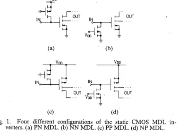
Four different configurations of CMOS MDL inverters are shown in Fig. l(a)–(d) where the names PN, NN, PP, and NP MDL are given to the corresponding configura-tions, respectively. As an illustrative example, only the PN MDL is analyzed in detail. Other configurations can be analyzed by using the same method.
In the PN MDL shown in Fig. 2, the transistor MN is a multidrain NMOS with its drain terminals connected as output nodes and its gate as the input node. The transistor MP is a PMOS which serves as a pull-up current source for the input node of transistor MN and the output node of transistor &f~P. Since the gate of transistor MP is grounded and the substrate is connected to the source, the available charging current is large without any degradation due to body effect.
If the NMOS MMP in the preceding stage is OFF, ~.~ is pulled up by the PMOS MP and the NMOS MN is turned
(a) — (b) “q OUT L & (c) (d)
Fig. 1. Four different configurations of tie static CMOS MDL in-verters, (a) PN MDL. (b) NN MDL. (c) PP MDL. (d) NP MDL. VDD . . . .
..’++J&#j~L
_J/_5
,...
Fig. 2. The basic structure of CMOS PN MDL inverters.
on. Thus the output voltage VO is pulled down. On the other hand, if the NMOS M~r is ON, ~.~ is pulled down. This turns off the NMOS MN and VO is pulled up by the PMOS MP~ in the load stage. This is the inverter oper-ation.
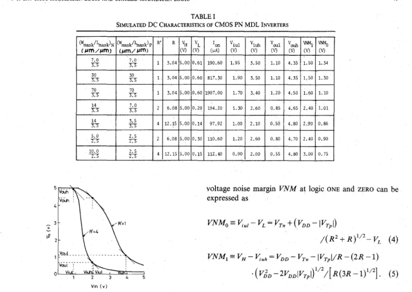
Typical transfer characteristics of the CMOS MDL are shown in Fig. 3 for different values of R’
-(W/%ask)N/(W/&ask)~. According to different operat-ing regions of the MOSFET’S MN and MP~, the whole characteristic can be divided into four regions and can be approximately modeled by using the first-order current equations. The detailed calculation is described in the Appendix. The voltages VH and V~ in the logic ONE and ZERO states, respectively, can be written as
VH= VDD
(1){
VL=
R(vDD–v,n)–lv,pl– [( RVDD– RV~n–lV,pl)2-(R
-l)(F%
-M’i)WTpl)]’’2)/(R
-1),
for V~ > IVTPI (2a)
=
VDD- vTn- [(vDD- vTn)2-(vDD- lvTJ/R]l’2,
for V~ < /V~pl (2b)
where R - p.( W/L) ~Con/[pp ( W/L )PCOP]. Generally, the value of R must be designed such that V~is smaller than v. In this case, the NMOS in the next stage can be tu%ed off when V.= V~.According to this design rule, the
WU et a[.: CMOS MULTIDWHN LOGICAND STACKED MULTIDRAIN LOGIC 49
Fig. 3. Transfer
TABLE I
SIMULATED DC CHARACTERISTICSOF CMOS PN MDL INVRRTERS
cwmwkl~m~)~ [wm~k&& P R’ R ‘H ‘L Ion ‘iul ‘iuh Voul Vouh Ml w
fw%z~m) (~m/ ~m:~ (w (w (MA) (W co (v) (w (w (w 7.0 % n 1 3.04 5.00 0.61 190.60 1.95 3.50 1.10 4.35 1.50 1.34 30 n % 1 3.04 5.00 0.60 817.30 1.90 3.50 1.10 4.35 1.50 1.30 % $5 1 3.04 5.00 0.60 1907.00 1.70 3.40 1.20 4.50 1.60 1.10 & H 2 6.08 5.00 0.29 194.20 1.30 2.60 0.85 4.65 2.40 1.01 +!s i% 4 12.15 5.00 0.14 97.92 1.00 2,10 0.50 4.80 2.90 0.86 2.5 E z-s 2 6.08 5.00 0.30 110.60 1.20 2.60 0.80 4.70 2.40 0.90 10.0 m i% 4 12.15 5.00 0.15 112.40 0.90 2,00 0.55 4.80 3.00 0,75 L 3 2 -YW! . . . . 1 ~ Vcul : ,! o 1 2 3 4 5 Vin (v)
characteristics of PN MDL inverters with different values of R’.
minimum required R ~ is approximately determined by
{ Rtin = – (V’’~/2 – 2V;. + VDDV~n– VDDIV&l+ V#~pl) [ + ( v;D/2 – 2v;n + v’Dv~n – vDDp~Tpl+ vTn[vTpl)2 – VTn(2VDD – 3VTn )( J’& – % ‘+ ZVTnlVTPl -2 VDDIVT,I)] 1’2}/[vTn(2vDD - 3VT.)] , for V~n > lV~pl (3a) Rti= (VDD – lv~pl)2/’[v,n(2vDD –
3vTn)1
~
for V~n < lV~p1. (3b)As maybe calculated from (3), the corresponding value of the geometrjc ratio R’ is about 0.9 for a typical CMOS process.
The voltages ~.Ul, ~.Uh, Voul, and V&k at unity-gain points indicated in Fig. 3 can be characterized by finding the slope of the transfer characteristic. Detailed calcula-tions are given in the Appendix. From (10) and (12), the
voltage noise margin VNM at logic ONE and ZERO can be expressed as
VNMO = ~ul – v~ = v~n + (VDD –
IV+)
/(R’ + R)l/2- V. (4)
. (V;D -2 VDDlVTpl)1’2/[R(3R -1)1’2] . (5)
Note that the MDL circuits are ratioed. Hence, the noise’ margin is not as good as that of the conventional CMOS logic. Its value depends cm the ratio 1? Wd the voltage V~
in the logjc ZERO state.
Table I lists the SPICE simulated dc characteristics of CMOS PN MDL inverters with different R’. For R’= 1,
V~ < V~nand VNMO = VNM1. This means the logic state is
stable and the transfer curve is nearly symmetric when
R’ =1. As compared with SPICE simulations, hand
calcu-lations using the above derived equations have an error less thap 20 percent if the mobility degradation is consid-ered. Thus these equations can bc used as good design guidelines.
AS to the connections among the four MDL configura-tions, the output node from an NMOS (PMOS) driver cannot be connected to the input node with an NMOS (PMOS) current injector because there will be no charging (discharging) path to the node. The PN MDL therefore cannot be connected to the NP MDL and so on. For those nodes where an NMOS driver and a PMQS current injec-tor are connected together, the ratio R‘ maybe as small as 1 according to (3). On the other hand the ratio R’ must be about 0.1 to obtain an outp~t voltage h@er than V~~ –
lV~pl at the node where an NMOS current injector and a
PMOS driver are connected. This leads to a larger PMOS channel width and thus a larger total chip area in both NP and PP configurations.
50 IEEE JOURNAL OF SOLID-STATE CIRCUITS, VOL. SC-22, NO. 1> FEBRUARY 1987 , --- ~ , (
L~...
l%;
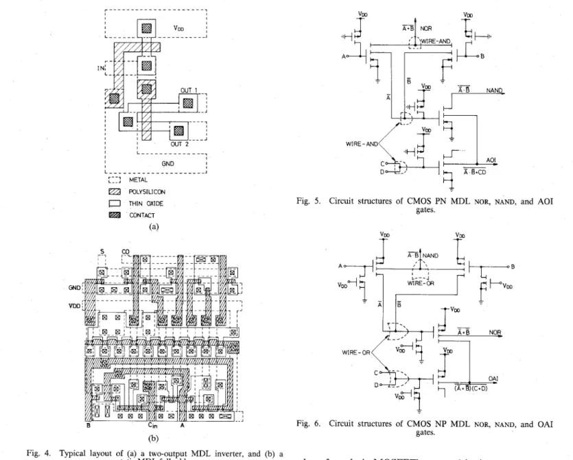
VDD L______ . . . IN . J . ( OUT 2 ‘ I L–--.-.–.--__––. , ! I GND I L-_--- __--- _--- _J__-_. J [z:] METAL n FOLYSILICON ~ THIN OXIDE ~ CONTACT (a) SC(I GND VDO B Cin A (b)Fig. 4. Typical layout of (a) a two-output MDL inverter, and (b) a static MDL full adder,
IIL PERFORMANCE EVALUATION FOR STATIC MDL
A. Logic Function and Chip Area
A typical layout diagram of a PN MDL inverter with two drain nodes is shown in Fig. 4(a) where the separation region between two drains is the field oxide region. Al-though a multidrain transistor is formed by connecting the sources of several MOSFET’S together, it is not too area consuming due to the compactly merged structure. More-over, it can be conveniently implemented in gate-array design. Generally, the chip area A,,a of a multidrain PN MDL is empirically determined by
Are a= (1+0.38N)F2 (6)
where N is the fan-out (drain) number and F is the minimum feature size. Based on 2-pm CMOS rules, the layout of a static PN MDL full adder is drawn in Fig. 4(b)
A
LLL
r.“4
!,(J
L... Vm WIRE-AND kaFig. 5. Circuit structures of CMOS PN MDL NOR, NAND, and AOI gates.
Vccl
VCQ
T-
-?-Fig. 6. Circuit structures of CMOS NP M.DL NOR, NAND, aud OAI gates.
where four-drain MOSFET’S are usedl for inputs A, B, and Cin.
Since the WIRE-AND or DOT-AND function can be implemented by tying the output nodes together, complex logic functions can be realized by PN MDL as shown in Fig. 5 where NAND, NOR, and AOI circuits are drawn. Due to the multidrain structure, all the ‘WIRE-AND functions can be efficiently formed without any interference am~ng them. Similarly, the NP MDL can be used to implement NAND, NOR, and OAI gates, as illustrated in Fig. 6, through the WIRE-OR connections.
Without the multidrain structure, the transistors MN and MP~ in Fig. 2 form a NMOS-like or pseudo-NMOS inverter. Similarly, the PN MDL NOR gate in Fig. 5 is the same as a NMOS-like NOR gate. However, due to the inherent multidrain and WIRE-AND capability, the MDL in general is different from the N MOS-like logic, and complex gates like NAND and AOI can be more efficiently realized with higher density and speecl in PN MDL than in NMOS-like logic. Similar features exist between NP MDL and PMOS-like logic. In the following analysis, compari-sons among these logic circuits will be given.
WU et al.: CMOS MULTIDRAIN LOGIC AND STACKED MULTIDRAIN LOGIC 51
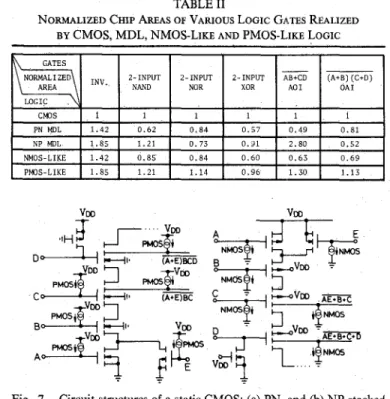
TABLE II
NORMALXZSDCHXPAREASOFVARIOUS LOGIC GA,TESREALIZED BY CMOS, MDL, NMOS-LIKE AND PMOS-LIRE LOGIC
LOGIC Ct.m PN MDL 1.42 0.62 0.84 0.57 0.49 0.81 NP MDL 1.85 1.21 0.73 0.31 2.80 0.52 NMOS-LIKE 1.42 0.85 0.84 0.60 0.63 0.69 PH3S-LIKE 1.85 1.21 1.14 0.96 1.30 1.13 TABLE III
NORMALIZED AVERAGE DELAY TIMES OF CMOS AND PN MDL INVERTERS UNDER DIFFERENT CONDITIONS
CONOITIONS Voo = 5V VDD = 5V VDO = 5V W7D = 5V Wo . w Vlm . 51J CL =OPF CL =OPF CL = OPF LOGIC
CMOS 1 1 1 1 1 1
PN MDL 0.63 0.82 0.83 0.56 0.83 0.S9
B. Speed and Power
Since the characteristic waveform is the actual internal voltage waveform within an IC chip, it is better to evaluate the speed performance of various logic gates by character-istic waveform timing. To obtain the characteristic wave-forms and their signal timing, a string of identical gates is excited and the output nodes of the intermediate stages are observed. In the following comparisons, the average delay time of a gate is defined as half of the pair delay in the characteristic waveform case.
The average delay times of various PN MDL inverters Fig. 7. Circuit structures of a static CMOS: (a) PN, and (b) NP stacked with different geometric ratio R‘ were simulated by using
MDL. the conventional CMOS device parameters. It is found
Based upon the same design rule, the layouts of various gates implemented by CMOS, PN MDL, NP MDL, NMOS-like and PMOS-like logic were generated. Their chip areas are compared in Table II where the area of each standard CMOS gate is normalized to unity. From this table it is seen that NAND and AOI gates ci~n be efficiently implemented by PN MDL with less chip area and NOR and OAI gates by NP MDL.
Since the voltage levels of MDL are. compatible with those of CMOS, a MDL gate without current injector can be driven directly by a CMOS gate. Similarly, by adding a current injector to the output node, a MDL gate can directly drive a CMOS gate. In these. cases, no interracial buffer is needed. However, a PP or NN MDL gate is needed between PN MDL and NP MDL gates.
Both PN MDL and NP MDL can be stacked to form NAND and NOR gates, respectively, as shown in Fig. 7. To keep the same ON resistance, the channel width of each stacked MOS must be enlarged. Due to the multidrain capability of the SMDL, the output can be taken from the drain of the intermediate MOS to form another logic function. As may be seen from the illustrative circuits shown in Fig. 7, two functions can be formed in “one” gate structure. By using such highly merged structures, the interconnection complexity can be reduce{d and the pack-ing density can be drastically increased. These lead to reductions in both interconnection delay and chip area, respectively. Such advantageous features are more signifi-cant in dynamic circuits, as will be seen later.
As compared to NMOS-like or PMOS-like logic, SMDL generally has higher design versatility as well as the above mentioned advantages, all due to its inherent multidrain capability.
that for the same current injector, ~he inverters with R‘ = 1 have smaller delay than those with R’> 1, because of the smaller size of the NMOS which leads to a smaller load capacitance. In the following comparisons, only R‘ =1 is considered.
By using the same p-well CMOS device parameters, the SPICE simulated average delay times of PN MDL and standard CMOS inverters with different capacitive loads, power supply voltages, arid channel lengths are compared in Table III where all the delay times are normalized. In this comparkon, the CMOS inverters are optimally de-signed such that the rise time is nearly ,equal to the fall time and the delay time is minimum. Furthermore, the total channel area of the PN MDL inverter is set to be equal to that of the CMOS inverter. In this case, the delay time of the PN MDL inverter is found to be 0.56–0.83 times as small as that of the CMOS inverter, even when the capacitive load is large, the channel length is scaled down to 2 pm, or the power supply is scaled down to 3 V. If the n-well or doutile-well CMOS technology is adopted, the delay time of the PN h4DL inverter is expected to be smaller because the p-n junction capacitance is decreased.
The simulated average delay times of inverters and three-input NOR gates implemented by CMOS, PN MDL, NP MDL, enhancement\depletion NMOS, NMOS-, and PMOS-like logic are compared in Table IV where the 3.5-pm device parameters are used. It is seen that even for complex gates, the PN MDL is still faster than other logic families, especially the CMOS logic. For the NP MDL, the speed is two times as slow as that of the PN MDL because of the large size of the PMOS driver.
To investigate the speed change due to the multidrain structure and the WIRE-AND connections, the average delay times of PN MDL inverters as a function of the number of drain nodes N and the number of WIRE-AND
52 IEEE JOURNAL OF SOLID-STATE CIRCUITS, VOL. SC-22, No. 1, FEBRUARY 1987
TABLE IV
NORMALIZED AVE&GE DELAY TIMES OF INVSRTERSAND THREE-INPUT NOR GATESREALIZED BY CMOS, MDL, E/D
NMOS, NMOS- AND PMOS-LIKE LOGIC
LOGIC NORMAL I ZED
CMOS PN MDL NP hQL E/D NM3S NNOS PMOS
DELAY -LIKE -LIKE
GATEs INVERTER 1.59 1 2.56 1.40 1.00 2.56 3-INPUT NOR 3.47 1 2.0s 1.3s 0.97 7.86 3-INPUT NAND 2.44 1 2.05 1,43 2.35 2.04 4 N.4 , M=l {0 Voo . 5V (Lmask.3.5ym) x VCO .5V z N.4, M.1 { v VW<5V z 10 (linask=2pm) * vm .5v w N=l ,M=l b 1.rm5k =3.5pm (vDD~
5V) {0
Lmask.2um ~’; ‘ \ ; > < 0.5 -,\ ,, 0.1 1 10 lCSI lm xcomAVERAGE CURRENT ( flA)
Fig. 8. The average delay times as a function of the average injector current for MDL inverters with different channel lengths and power supplies.
inputs M were found by simulation. The normalized aver-age delay times are
r~=l+O.23N 7M=1+0.57M.
Note that the increase in the delay time due to an extra output drain node is very small.
The average delay time of PN MDL inverters with N = 4 as a function of the average injector current is shown in Fig. 8 where the average current is equal to half of the maximum injector current in the logic ZERO state because no current flows in the logic ONE state. Also shown in Fig. 8 is the average time of PN MDL inverters with N =1, R‘ =1, and scaled-down power supply. From this figure it is seen that the speed of MDL is quite comparable with that of I ‘L [2] or even ECL [6]. More-over, the minimum power–delay product of the MDL is in the range of 0.02–0.1 pJ for 2-pm CMOS process. This value is smaller than the typical values of 0.5 –1.8 pJ in ECL [6] and 0.02–0.6 pJ in 12L [6] and is nearly the same as that of l-pm standard CMOS logic [1] under 300-MHz operations. However, unlike the standard CMOS logic, the CMOS MDL has dc power dissipation.
From the above analysis, it is realized that the incorpo-ration of MDL in a CMOS chip can promote the speed performance to the bipolar level while keeping the same power–delay product and the same process complexity of CMOS. It is expected, therefore, that the application field of CMOS can be extended to that of bipolar.
‘h T
-d
::.2!...
—...
*I.3
MB 4 Mult idm!n M2 C@Jts 7 L.. -... (c) (d)Fig. 9. Circuit structures of (a) a dynamic NN MDL inverter, (b) a dynamic PP MDL inverter, (c) a dynamic SMDL gate based on the NN configuration, and (d) a dynamic SMDL gate based on the PP config-uration.
IV. DYNAMIC MDL AND SMDL
The NN and PP MDL configurations can be used to construct the dynamic circuits to reduce the dc power dissipation. The basic dynamic MDL structures are drawn in Fig. 9(a) and (b) where @= 1 is the precharging phase and ~ = O is the evaluation phase. The precharging device Md is used to pull up or pull down the output voltage. It also serves as the input precharging device of the next stage. Similarly, the MOS Ml is the input precharging device of this stage and is the output precharging device of the preceding stage. In the circuit of Fig. 9(b), the geomet-ric ratio R‘ of the PMOS ikf~ to the NMOS 341 may be unit y.
The SMDL structures of Fig. ‘7 can also be converted into dynamic circuits as shown in Fig. 9(c) and (d). In this diagram, the output precharging devices are not shown. According to the analysis in Section II, these dynamic NN and PP configurations in Fig. 9 must be alternatively connected. Therefore both dynamic MDL and dynamic SMDL circuits have no internal race (glitch) problems, like the DOMINO [7] or the NORA-CMOS [8] techniques. Basically, the dynamic MDL and SMDL circuits are simil-ar in sttucture to the other two dynamic circuits except that the dynamic MDL and SMDL have multidrain capa-bility. Due to such inherent multidrain connections, many Boolean tefms among various logic functions can be real-ized and merged together in a dynamic SMDL gate as shown in Fig. 9(c) and (d). In these illustrative circuits, three extra Boolean terms can be implemented by adding three extra drain nodes to the original dymimic AOI/OAI
WU et al.: CMOS MDLTIDRAIN LOGIC AND STACKED MDLTIDRAIN LOGIC
TABLE V
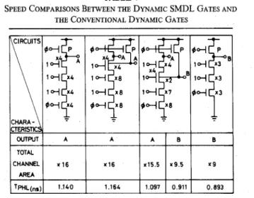
SPEEDCOMPARISONSBETWEENTHE DYNAMIC SMDL GATESAND THE CONVENTIONAL DYNAMIC GATES
D
CIRCUITS @+ P 14 A lq Xh 1+ x4 $+ Xri CHARA - = CTERlsk
OUTFUT A TOTAL CHANNEL x16 AREA ‘PWns) 1.140 1.164 1.097 0.911 I 0.893 ]gates and suitably enlarging the channel widths of the related MOS’S. There is no need to separately construct three extra gates. Therefore the interconnection complexity for input signals is reduced. Meanwhile, the packing den-sit y is improved due to the highly merged structure.
To investigate signal “speed and channel-width design in a dynamic SMDL gate, SPICIj simulations on the fall delay time TPH~ of various PN dynamic SMDL gates excited by an evaluation clock @with 1.6-ns rise time were performed. Some of the results are listed in Table V where the delay times of the corresponding conventional dynamic gates are also given for comparison. It is seen that if the multidrain structure is formed in the output NMOS, the channel widths of the other three NMOS’S must be dou-bled as shown in the second circuit of Table V. As com-pared with the corresponding conventional dynamic gate, the total channel area is the same and the delay time is also the same. If the multidrain structure is formed in the second upper NMOS as shown in the third circuit, suitable width design still leads to the same total channel area and nearly the same speed. Generally, the gate speed character-istics “of the dynamic SMDL are similar to those of con-ventional dynamic circuits.
To illustrate more clearly the advantageous features of the dynamic SMDL, a dynamic lookahead carry generator for a dynamic 4-bit full adder is designed and shown in Fig. 10(a) where the circuits used to generate ~i and ~i are not drawn out. As compared with the conventional design which implements C2, C~, and CA separately using dy-namic AOI/OAI gates as shown in Fig. 10(b), the design in Fig. 10(a) is much more compact due to the multidrain capability which merges many devices together.
The layout of bofi circuits was generated according to 2-pm CMOS design rules. The layout of the dynamic SMDL lookahead carry generator in Fig. 10(a) is shown in Fig. 1O(C). As compared with the layout of the conven-tional CMOS design, the chip area of the SMDL design is only 58 percent that of the CMOS design. This is due to the highly merged structure and the simple interconnec-tion, as can be seen from Fig. 1O(C). Generally, less inter-connection complexity also leads to smaller delay. Such
L L 1 1 I $+ ’’X24 T~ (a) 53 (c)
Fig. 10. (a) Circuit structure of a dynamic SMDL lookahead carry generator. (b) Circmt structure of a dynamic CMOS lookabead carry generator. (c) Layout of the dynamic SMDL lookahead carry generator based on 2-~m CMOS design rules.
advantageous features become more significant in VLSI design where interconnections dominate both packing den-sity and signal delay.
V. EXPERIMENTAL RESULTS
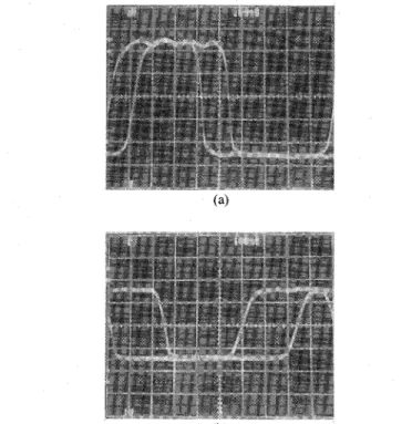
One string of ten identical static PN MDL inverters and one string of ten identical standard CMOS inverters were designed, fabricated, and measured. The output node of
54 IEEE JOURNAL OF SOLID-STATE CIRCUITS, VOL. SC-22, NO. 1, FEBRUARY 1987
(a)
(b)
Fig. 11. Measured characteristic waveforms of the fabricated PN MDL inverters with (a) V~~ = 5 V, and (b) V~~ = 3V.
TABLE VI
EXPERSMSNTALLYMEASUREDAVERAGEDELAY TIMES OF PN MDL AND CMOS INVERTERS
VDD GATE TP F TPR (n.) LTPF”TPR)/Z (ns) (ns) MDL/CWIS 5V PN MDL 103.5 -121,5 111.3 -125.0 107.6 -120.1 CMOS 129. 3-149.6 132.4 -159.4 130. 9-154.5 0.82 0.78 3V PN MDL 236.3 -265.6 233. 4-245.1 240. 7-25D. D CMOS 325.2 -338.9 324. 2-335.9 324.7 -337.4 0.72 0.77
each inverter is connected to a bonding pad through a CMOS buffer. Due to the buffer action, the output load capacitance in each inverter is nearly the same even when the output bonding pads of the fifth and seventh inverters are connected respectively to two FET probes with 2-pF input capacitance. By using such an arrangement, there-fore, the characteristic waveform timing can be measured through the FET probes.
Typical measured characteristic waveforms of the PN MDL inverters which were designed and fabricated by using 5-pm p-well CMOS technology are shown in Fig Ii(a) and (b) with V~~ = 5 and 3 V, respectively. The two waveforms in each figure are identical because they are measured from the outputs of the fifth and seventh stages. The pair delay Tp~ ( TP~) between two fall (rise) wave-forms thus can be measured directly. The results are listed in Table VI where the corresponding data of standard CMOS inverters are also given. It is seen that the mea-sured delay times of static PN MDL inverters are about 0.72-0.82 times as small as those of standard CMOS inverters. These experimental observations, therefore, are consistent with the theoretical predictions described in Section III.
VI. DISCUSSION AND CONCLUSION
A novel logic in CMOS technology called the CMOS multidrain logic (MDL) is proposed, analyzed, and experi-mentally observed in this study. In the static CMOS MDL, four different configurations are available in logic design and complex logic gates are formed through the use of WIRE-AND and WIRE-OR capabilities in PN and NP configurations, respectively. Due to the wire logic and the multidrain capabilities, the average area per gate is smaller in the MDL than in the conventional CMOS. Further-more, the minimum delay of a PN MDL inverter with single fan-in and fan-out is about 200 ps in 2-pm CMOS technology. This speed performance is comparable to that of 12L or even ECL and is about 20–70 percent better than that of the conventional CMOS. The power–delay product is nearly the same as that of the conventional CMOS under 300-MHz operations but is smaller than that of 12L and ECL. Therefore the static CMOS MDL can be used to increase the signal speed while keeping the same power–delay product as the conventional CMOS. Meanwhile, it is expected that the static CMOS MDL can be designed to achieve the bipolar speed level with smaller power–delay product and smaller dc power dissipation.
The static CMOS MDL can be stacked to form the stacked MDL (SMDL). Both PP and NN configurations in the MDL and the SMDL can be converted into dynamic circuits. They have no glitch problems. Moreover, due to the inherent multidrain structure which can be used to realize many Boolean terms within a highly merged dy-namic SMDL gate, the resultant circuits have higher pack-ing density and lower interconnection complexity than other CMOS dynamic circuits. These advantageous fea-tures make the dynamic CMOS SMDL a potential tech-nique in CMOS VLSI design.
Based upon the results in this study, it is felt that the bipolar-competitive MOS VLSI can be designed by using the bipolar-like CMOS logic circuits. Further research in this direction will be done.
APPENDIX
According to different operating regions of the con-sistent MOSFET’S in the PN MDL inverter shown in Fig. 2, the transfer characteristic of Fig. 3 can be divided into four regions. In Region I, ~.~ = V~ < VT. and the NMOS
MN is OFF. We have
1~~= O VO=VH=VDD.
In Region II, O < ~.~ – V~~ < VO. In this region, MN is in the saturation region whereas the PMOS MP~ is in the linear region. Thus we have
Id. = Pncon(w/L)iV(hI – ~Tn)2/’2
[
= Idp = Ppcop(~/~)p 2(VDD – /~Tpl)
WU et a[.: CMOS MULTIDRAIN LOGIC AND STACKED MULTIDRAIN LOGIC 55
REFERENCES The output voltage VO can be solved from the above
equation as
v-o= – IVTP[+ ([ VTPI– VDD)2– ~(v,, – J%)2 . (7)
In Region III where ~. – VT. > ~, > IV~Pl, both MOSFET’S are operated in the linear region. The current can be written as
Idn=&Gn(w\mv[wL-J7T.)JL–
J?l\2
[
=Idp=Ppqp(~/’~)P
2(J%D
–
W’pl)
.(vDD-vo)-(vDD- vo)2]/2.
Solving the above equation, we have
{
‘o=
‘( Kn-vTn)
-lvT,l-([lvTpl-
R(Jjn-vTn)]2
-(R
-l)(V;D
-2vJvTpl)}’’2}/(R
-1).
(8)In Region IV, VO< lV~.1 and VO< ~. – V~.. Thus MN is in the linear region and’ MP~ is in the saturation region. From the current relation which can be similarly written out, VOcan be solved as
Z?=zn -~nl -
[(%
-b)’-(h)-
lvTpl)2/R]l’2.
(9)
It may be seen from (9) that Region IV exists only when VT. < Vml – (J(DD - l~Tpl)/’@’2.
To find V~, ~.~ in (8) and (9) must be replaced by V~~ ( = V’). The resultant expression is shown in (2).
One of the unity-gain points defined at the point of fiUl and V’oUl is located in Region II. By taking the first derivative of (7) and setting it to unity, F(U1 and VOUkcan be expressed as
~ul = vTn +
(vDD– [F’Tpl)/(R’+
R)l’2
(lo)v
ouh = - lVTpl+ (k- IvTpl)[R/(fi! +1)]1/2. (11),The other unity-gain point denoted by ~Uh and VOU1is
located in Region III. By using the similar method, ~Uk and VOU1can be written as
yUh = V,n + lV,P1/R +(2R –1) o[(V’D – 2VDDlV~Pl)/(3R – I)] 1’2/’R (12) -( R-l)(V;D -2VDDIVTPI))1’27(R -l). (13) [1] [2] [3] [4] [5] [6] [7] [8] [9] [10] [11] [12] [13] [14] [15] [16] [17]
T. Yamaguchi, S. Morimoto, G. H. Kawamoto, and J. C. Delacy, “Process and device performance of l-pm channel n-well CMOS technology,” IEEE J. Solid-State Circuits, vol. SC-19, pp. 71-80, Feb. 1984.
S. K. Wiedmann, “Advancements in bipolar VLSI circuits and technologies.” ZEEEJ. Solid-State Circuits, vol. SC-19, PP. 282–291, June 198%
K. Yu, R. Chwang, M. T. Bohr, P. A. Warkentin, S. Stern, and C. N. Berglund, “ HMOS-CMOS—A low-power hrgh-performance technology,” IEEE J. Solid-State Circuits, VO1. SC-16, PP. 454–459, Oct. 198i:
J. P. Victorey and J. C. Vesely, “A two micron double-level-metal CMOS technology,” in Proc. 1982 Custom Integrated Circuits Conf., May 1982, pp. 85-89.
I. %kai, O. Kudoh, and H. Yamrrmoto, “High speed 1 pm CMOS technology,” in Tech. Dig. 1982 IEDM, Dec. 1982, pp. 702-705. S. Tanaka, J. Iwamura, J. Ohno, K. Maegucli, H. Tango, and K. Doi, “A subnanosecond 8K-gate CMOS/SOS gate array;’ IEEE J. Solid-State Circuits, vol. SC-19, pp. 657-663, Oct. 1984.
R. H. Krambeck, C. M. Lee, and H. S. Law, “High-speed compact circuits with CMOS,” IEEE J. Solid-State Circuits, vol. SC-17, pp. 614-619, June 1982.
N. F. Goncalves and H. De Man, “NORA: A racefree dynamic CMOS techniaue for ~iDeline loszic structures.” IEEE J. Solid-State Circuits, vol. SC-18, ~p~261-26X, June1983
V. Friedman and S. Liu, “Dynamic logic CMOS circuits;’ IEEE J. Solid-State Circuits, vol. SC-19, pp. 263-266, Apr. 1984.
L. G. Heller, W. R. Griffin, J. W. Davis, and N. G. Thoma, “ Cascode voltage switch logic: A differential CMOS logic family,” {n Int. Solid State Circuits Corrf. Tech. Dig., Feb. 1984, pp. 16–17. J. R. Pfiester, J. D. Shott, and J. D. Meindl, “E/D CMOS—A high speed VLSI technology,” in Proc. IEEE 1983 Symp. VLSI Technol., pp. 44-45.
A. K. Goksel, J, A. Fields, F. D. LaRocca, P. M. Lu, W. W. Troutman, and K.-N. Wong, “A VLSI memory management chip: Desire considerations and ex~erience.” IEEE J. Solid-State Cir-cuih~vol. SC-19,pp. 325–3281June 1984.
R. J. Baumer!, L. E. Cameron, and R. A. Wilson, III, “A mixed EFL 12 L di@al telecommunication integrated clrcuity IEEE J. Solid-State Circuits, vol. SC-19,pp. 26-31, Feb. 1984.
A. Mohsen. R. I. Kumz. C. U. Simonsen. J. Schutz. P. D. Madland. E. Z. Hamdy, and M~T. Bohr, “The design and’ performance of CMOS 256K bit DRAM devices,” IEEE J. Solid-State Circuits, vol. SC-19, pp. 610–618, O(X.1984.
L. F. Childs and R. T. Hirose, “An 18 ns 4Kx4 CMOS SRAM,” IEEE J. Solid-State Circuits, vol. SC-19,pp. 545-551, Oct. 1984. M. I. Elmasry, “ Multidrain NMOS for VLSI logic design,” IEEE Trans. Electron Devices, vol. ED-29, pp. 779-781, Apr. 1982. M. I. Elmasry, “Nanosecond NMOS VLSI current mode logic,” IEEE Trans. Electron Devices, vol. ED-29, pp. 781-784, Apr. 1982.
Chrmg-Yu Wu (S’75-M77) was born in Chiayi, Taiwan, Republic of China, on May 31,1950. He received the B.S. degree from the Department of Electrophysics, and the M.S. and Ph.D. degrees from the Institute of Electronics, National Chiao-Tung University, Hsinchu, Taiwan, Re-public of China, in 1972, 1976, and 1980, respec-tively.
During 1975–1976, he studied ferroelectric films on silicon and their device applications. During 1976-1979, he engaged in the develop-ment of integrated differential negative resistance devices and their circuit applications, with support from the Nationaf Electronics Mass Plan (Semiconductor Devices and Integrated Circuit Technologies) of the National Science Council. From 1980 to 1984 he was an Associate Professor at the Institute of Electronics, Nationaf Chiao-Tung University. During 1984–1986 he was an Associate Professor in the Department of Electrical Engineering, Po@md State University, Portland, OR. Pres-ently he is Professor in the Department of Electronics Engineering and the Institute of Electronics, Nationaf Chiao-Tung University. His re-search interests have been in device modeling, integrated-circuit technolo-gies, semiconductor memories, analog integrated circuits, digital in-tegrated circuits, and computer-aided circuit design.
56 IEEE JOURNAL OF SOLID-STATE CIRCUITS, VOL. SC-22, NO. 1, FEBRUARY 1987
Jinn-Shyan Wang was born in Yuen-Lin, Taiwan, Republic of China, in 1959. He received the B.S. degree in electrical engineering from National Cheng-Kung University, Tainan, Taiwan, in 1982 and the M.S. degree in electncaf engineering from National Chiao-Tung University, Hsin-Chu, Taiwan, in 1984. Currently, he is working toward the Ph.D. degree at Nationaf Chiao-Tuug Uni-versit y. His research field is in integrated-circuit design,
Ming-Kai Tsai (M82) was born in Ping-Tung, Taiwan, Republic of China, in 1950. He received the B.S. degree in electrical engineering from National Taiwan University, Taipei, Taiwan, and the M, S. degree in electrical engineering from the University of Cincinnati, Cincinnati, OH, in 1971 and 1976, respectively,
During 1976–1983 he joined the Electronic Research and Service Organization, Industrial Technology Research Institute (ERSO, ITRI), Taiwan, where he was initially an MOS IC De-sign Engineer. He became the Manager of the Microcomputer IC Design Department in 1980. Since 1983 he has been Director of the Research and Development Department at United Microelectronics Corporation, Hsin-Chu, Taiwan, responsible for afl the research and development in MOS VLSI circuit and system design,