38
4-900784-01-X 2005 Symposium on VLSI Circuits Digest of Technical Papers3-3
Subharmonic Direct Frequency Synthesizer for
Mode-1 MB-OFDM UWB System
Chien-chih Lin and Chorng-Kuang Wang
Department of Electrical Engineering & Graduate Institute of Electronics Engineering National Taiwan University, Taipei, Taiwan 10617, R.O.C.
Abstract— This paper proposes a subharmonic direct fre-quency synthesizer (SH-DFS) for the hopping carrier generation in mode-1 MB-OFDM based UWB system. The SH-DFS employs octet phases of 2.244GHz from a VCO to synthesize and the deviations at 528MHz and 1.056GHz acquired from a divide-by-17 semi-dynamic divider. The output stage with the switched functionalities between a subharmonic single sideband (SH-SSB) mixer and an edge combiner generates the designated tone. Realized in 0.18-µm CMOS technology, it occupies an active area of 1×1 mm2. The chip draws 34mW power from a single supply at 1.8-V. The carrier output has the voltage swing larger than 700mVppand the spurious tones are smaller than -20dBc.
I. INTRODUCTION
Ultra-wideband (UWB) wireless transmission has the capa-bility of cable replacement in personal multimedia transmis-sion and is expected to provide high data-rate indoor wireless connectivity for computers, digital equipments, and mobile gadgets. Currently, multi-band orthogonal frequency division multiplexing (MB-OFDM) approach is the potential standard to map out the usage of the frequency band from 3.1GHz to 10.6GHz. It splits the 7.5GHz band into 14 sub-bands and assigns the hopping carrier to convey the 528MHz OFDM-modulated signals [1]. Aside from the large frequency spacing, the local oscillator needs to cope with high agility requirement; i.e., the hopping time from one carrier to the other should be less than 9ns. The common approach based on phase locked-loop (PLL) to generate the local oscillation signals would not be applicable here for the long settling time caused by the narrow loop bandwidth. Direct frequency synthesis (DFS), constructed by a single side-band (SSB) mixer to move a fixed oscillation signal to a designated frequency, can fit in this system specification. This paper discusses the carrier generation for mode-1 operation, which uses the first 3 sub-bands only, and proposes a subharmonic DFS to generate the mandatory carriers at 3.432GHz, 3.96GHz, and 4.488GHz.
To start with, the direct frequency synthesis calls for com-petent frequency planning that puts into consideration the circuit feasibility, hardware cost, interferences among different channels, etc. The straightforward approach using 4.224GHz as the base tone [1] may suffer from adjacent sub-band interference brought about by the cascading SSB mixers and close image frequencies. Using the semi-dynamic regeneration frequency divider, the base tone may be set at 3.96GHz with a view to mitigating the image contamination problem [2]. However, the output stage in [2], realized by a Gilbert-cell type
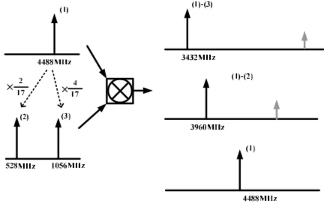
Fig. 1. Frequency translation scheme for the direct frequency synthesis
SSB mixer, still suffers from the leakage of the base tone at 3.96GHz, which causes interferences with adjacent sub-band. To further alleviate the spurs, this paper proposes the frequency translation scheme for the DFS that uses the base tone at 4.488GHz and the deviation frequencies at 1.056GHz and 528MHz, as shown in Fig.1. Besides from the less susceptibility to image contamination, it uses the subharmonic mixer as the output stage to reduce the leakage problem [3]. Section II discusses the frequency translation scheme and the circuit architecture. The circuit design and the measurement results of the SH-DFS are described in Section III and Section IV respectively. Finally, the conclusion is given in Section V.
II. SH-DFS ARCHITECTURE
The direct frequency synthesizer depends on a frequency translation circuit, usually an SSB-mixer, to place the output tone at a required position in the frequency domain. However, the intrinsic mixing operation suffers from image problems for the limited side-band rejection in real circuits. It is then expected to separate the desired tone and the image tone as far as feasible such that an auxiliary filter at the output may easily dispose of the image signal. Here the frequency planning scheme is based on the translation from 4.488GHz. The image frequencies locate at 5.016GHz and 5.544GHz respectively when 3.96GHz and 3.432GHz carriers are acquired. To deal with the leakage from the switching stage of the SSB mixer, the subharmonic mixer is used to realize the output stage. Fig. 2 shows the proposed architecture where the current commutating is performed by eight phases of oscillation signals at 2.244GHz from a built-in ring oscillator. When the
39
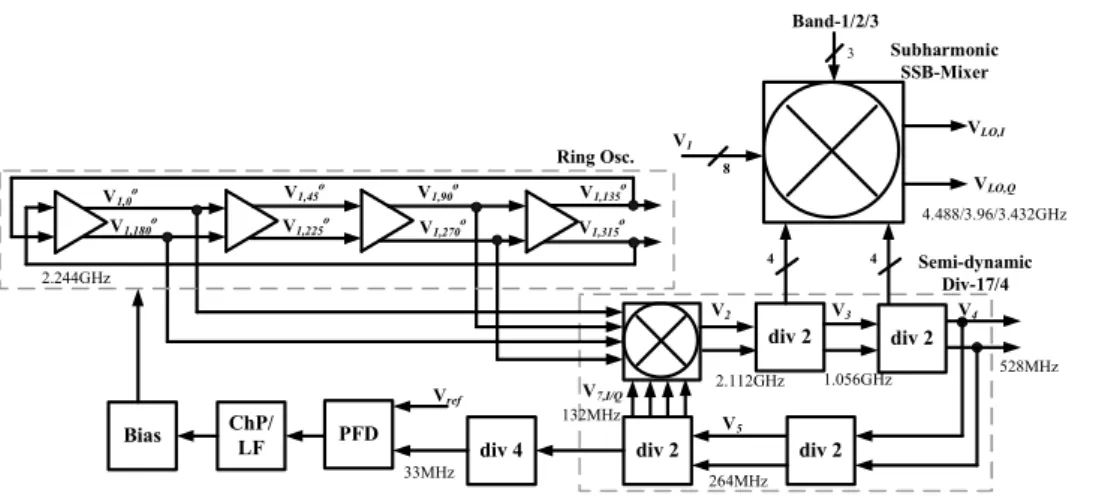
2005 Symposium on VLSI Circuits Digest of Technical Papers div 2 Band-1/2/3 Semi-dynamic Div-17/4 3 V4 V2 2.112GHz 1.056GHz V5 528MHz 264MHz V7,I/Q 132MHz VLO,I VLO,Q 4.488/3.96/3.432GHz Subharmonic SSB-Mixer V1,0o V1,180o V1,45o V1,225o V1,90o V1,270o V1,135o V1,315o 2.244GHz div 2 div 2 div 2 V3 V1 8 4 4 div 4 PFD Ring Osc. Vref 33MHz ChP/ LF Bias
Fig. 2. Subharmonic direct frequency synthesizer (SH-DFS) architecture
carrier frequency of 4.488GHz is required, the SH-SSB mixer turns into a phase combiner to recombine the 8 phases of oscillation signals.
The SSB mixer relies on the transconductance inputs with symmetric in-phase (I-) and quadrature-phase (Q-) sinusoidal waves as the frequency deviation to synthesize required tones. To derive 528MHz and 1.056GHz deviations from the 2.244GHz oscillator, the semi-dynamic regeneration loop [2] has been applied. It employs 4 stages of static dividers with an SSB mixer to form a divide-by-17 frequency divider. The deviations are drawn from the first and the second static dividers that have symmetric I/Q-waveforms. A multiplexer is embedded to select one of the deviation quads according to the band selection code. Besides of the assistance in carrier generation, the semi-dynamic frequency divider also provides system clock at 528MHz for the digital processing unit and 132MHz oscillating signal to assist the PLL loop operation.
III. CIRCUITDESIGN
The voltage-controlled ring oscillator (VCO) is composed of 4 stages of symmetric-loaded delay cells with self-bias circuitry [4]. Oscillating at 2.244GHz, the eight phases of sinusoidal waves feed to the built-in buffers to drive the SHSSB current switching octets and the semi-dynamic fre-quency divder.
To acquire deviation signals from the 2.244GHz oscillator, the semi-dynamic frequency divider in a regenerative loop is applied, as shown in Fig.3. Because of the availability of high swing oscillation from the VCO buffers, the passive mixer is used to configure the SSB mixer stage in order to lower down the power consumption and provide better linearity. Four current mode logic (CML) based static dividers are used to facilitate the operation with the first two of them contributing the deviation signals. Since the CML divider calls for only two out-of-phase clock signals, dummy devices are added at the outputs of the cascading cells to balance the loading effects and achieve better phase accuracy.
Before feeding the SH-SSB output stage, the two quads of deviation signals need to be selected according to the band
Fig. 3. Semi-dynamic frequency divider regenerative loop.
Fig. 4. Multiplexer circuit.
selection code. Therefore, two I/Q multiplexers (MUXs) are added each of which has inputs from I- or Q- channels of the first two CML dividers of the regenerative loop. The MUX is constructed by two differential pairs sharing the same diode loads. Attached in the paths from the transconductance
devices M1−4,I/Qtoward the loads M9−10,I/Qare the cascode
devices M5−8,I/Q which equip the MUXs for signal selection,
bandwidth extension, and isolation from the succeeding SH-SSB mixer. When band 3, i.e. 4.488GHz, is selected however, the MUXs are disabled by shutting down both the cascode devices.
40
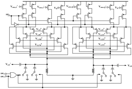
4-900784-01-X 2005 Symposium on VLSI Circuits Digest of Technical PapersThe output stage has the octave sinusoidal signals at 2.244GHz from the ring oscillator and the two pairs of quad deviation signals at 1.056GHz and 528MHz respectively from the regenerative divider loop. To generate the local oscillation (LO) signals at the specified three frequencies, a output stage with functionalities of SH-SSB mixer and edge combiner
is proposed as shown in Fig.5. Transistors Msw1−8,I/Q are
the subharmonically switching current commutators that boost the frequency of the current inputs from the sources toward twice their input frequency from the gates. The I-path takes
oscillation signals of 0o, 90o, 180o, and 270ophases, while the
Q-path takes 45o, 135o, 225o, and 315ophases. By combining
the I/Q current signals from the pair of switching quads in a certain polarity and injecting them into the loads, the single side-band frequency can be extracted in the same method as the traditional SSB mixer operation. To further suppress the image tones and spurs from circuit nonlinearity, a bandpass filter with switched center frequency is built which takes the band selection code to switch the capacitive loads in parallel with the inductor.
The current buffers Mbf 1−4,I/Q serve as the second stage
for frequency selection. When band 1 or band 2 are selected,
the PMOS devices Mbf 1,I/Q and Mbf 3,I/Q are turned on and
pass the frequency deviation signals from the MUXs toward the pair of switching quads. They also enhance the reverse isolation from the switching signals to the MUXs. When
band 3 is chosen, the PMOS devices Mbf 2,I/Q and Mbf 4,I/Q
are activated and delivers DC bias currents for the switching
quads. Here, only transistors Mbf 4,I/Qprovide source currents
whereas Mbf 2,I/Q are dummy devices. Half of the signal
paths of each switching quad will be shut down and the rest become combining the multiphase signals from the oscillators. The edge combination behavior under this condition serves as a frequency multiplier [5] and turns the octet 2.244GHz inputs into 4.488GHz LO signal. In cooperation with the high frequency selectivity LC output loads, the leakage from the gates of the switching quads into the output can be significantly suppressed.
IV. MEASUREMENT
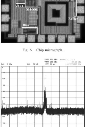
The subharmonic direct frequency synthesizer has been realized in 0.18-µm 1P6M CMOS technology. Fig.6 shows
the die microphotograph. The core area occupies 1×1mm2.
The GSGSG PAD is laid for the measurement of the SH-SSB outputs with the on-wafer differential probe. To measure the hopping carrier behavior, additional clock signal is required to trigger embedded shift registers that mimic a hopping time-frequency code (TFC).
The tested VCO, however, has lower oscillation frequency than designed. Due to process variation, it turns to be 2.05 GHz, which is 200MHz below the required value. When band 3 is selected, the output stage is switched to the edge combination operation. The measured spectrum is shown in Fig.7, where the output tone is twice the oscillation frequency. Fig.8 shows the result when the band selection code is changed to band 1. The measured frequency from the SH-SSB
Fig. 6. Chip micrograph.
Fig. 7. The spectrum of the output stage operating as an edge combiner.
mixer is 13
34-times the oscillation frequency, which verifies the
operation of the semi-dynamic frequency divider and the SH-SSB mixer. Observed by the sampling scope, the measured transient behavior in frequency hopping is shown in Fig.9. The settling time from each hop is about 2.4ns. The single sideband
voltage swing achieves larger than 100mVpp from the open
drain buffer. According to the simulation, this corresponds to the voltage swing of the output stage being about 700mVpp. The spurious tones at the image frequencies and harmonics are less than -20dBc. Table I summarizes the chip performance.
V. CONCLUSION
This paper presents a direct frequency synthesizer architec-ture and its circuit design. To improve the image and spurious suppression from the single sideband frequency translation, the base tone at 4.488GHz is used. It is further divided into 8 phases of 2.244GHz oscillation signals to cooperate with output programmable LC bandpass filter to avoid leakage. The subharmonic SSB mixer core is used to accommodate the octave oscillation signals and translate the deviation signals from the semi-dynamic degeneration frequency divider that
41
2005 Symposium on VLSI Circuits Digest of Technical Papers V1,0o V1,90o V1,180o V1,270o V1,45o V1,135o V1,225o V1,315o VB
Vmux,I+ Vmux,I- Vmux,Q+ Vmux,Q -sw3
VLO+ VLO
-VB
sw2 sw1
Fig. 5. Output stage with switching functionalities of subharmonic single-sideband mixer and edge combiner.
Fig. 8. The spectrum of the output stage operating as a subharmonic single sideband mixer.
provides 17
2 and 17
4 dividing ratios. The switching quads of
the SH-SSB mixer play as edge combination transconductance stages for the 4.488GHz LO generation when half of the branches are turned off. The switched SH-SSB/Edge-combiner provides the hopping carriers in mode-1 MB-OFDM UWB system.
ACKNOWLEDGMENT
The authors would like to acknowledge the research support of MediaTek Inc.
REFERENCES
[1] MultiBand OFDM Alliance SIG, ”Multiband OFDM physical layer proposal for IEEE 802.15 Task Group 3a,” Sep. 14, 2004.
[2] C.-C. Lin and C.-K. Wang, ”A semi-dynamic regenerative frequency divider for mode-1 MB-OFDM UWB hopping carrier generation,” in ISSCC Dig. Tech. Papers, sec. 11-4, Feb. 2005.
Fig. 9. Frequency hopping behavior.
Technology 0.18µm 1P6M CMOS Supply voltage 1.8 V Power consumption 34 mW Active area 1×1 mm2 Hopping speed <2.4ns Spurious <-20dBc Output swing >700mVpp TABLE I PERFORMANCESUMMARY
[3] K.-J. Koh, M.-Y. Park, C.-S. Kim, and H.-K. Yu, ”Subharmonically pumped CMOS frequency conversion (up and down) circuits for 2-GHz WCDMA direct-conversion transceiver,” IEEE J. Solid-State Circuits, vol. 39, pp.871-884 , June 2004.
[4] John G. Maneatis, ”Low-jitter process-independent DLL and PLL based on self-biased techniques,” IEEE J. Solid-State Circuits, vol. 31, pp.1723-1732, Nov. 1996.
[5] G. Chien and P.R. Gray, ”A 900-MHz local oscillator using DLL-based frequency multiplier technique for PCS applications,” IEEE J. Solid-State Circuits, vol. 35, pp.1996-1999 , Dec. 2000.