國 立 交 通 大 學
光 電 工 程 研 究 所
碩士論文
利用微米透鏡陣列與表面粗化加強垂直式
氮化鎵發光二極體發光強度
Light output enhancement of GaN vertical
light emitting diode using micro-lens array
and surface roughening
研
研
究
究
生
生
:
:
葉
葉
剛
剛
帆
帆
..指
指
導
導
教
教
授
授
:
:
王
王
興
興
宗
宗
教
教
授
授
郭
郭
浩
浩
中
中
教
教
授
授
中
中
華
華
民
民
國
國
九
九
十
十
五
五
年
年
六
六
月
月
利用微米透鏡陣列與表面粗化加強垂直式氮化鎵發光二極
體發光強度
Light output enhancement of GaN vertical light emitting diode
using micro-lens array and surface roughening
研究生:葉剛帆 Student : Kang-fan Yeh
指導教授:王興宗 教授 Advisor : Shing-Chung Wang
郭浩中 教授 Hao-chung Kuo
國 立 交 通 大 學
光電工程研究所
碩 士 論 文
A Thesis
Submitted to Institute of Electro-Optical Engineering College of Electrical Engineering and Computer Science
National Chiao Tung University in Partial Fulfillment of the Requirements
for the Degree of Master
In
Electro-Optical Engineering
June 2006
利用微米透鏡陣列與表面粗化加強垂直式氮化
鎵發光二極體發光強度
研究生:葉剛帆 指導教授:王興宗 教授
郭浩中 教授
交通大學光電工程研究所
摘要
在本篇論文中,主要是探討垂直式氮化鎵發光二極體在表面製作微米透鏡陣 列與表面粗化的製成技術與特性量測。在第一部分,我們利用雷射剝離技術成功 的製做出垂直式氮化鎵發光二極體,並且在利用光阻溢流與乾式蝕刻將微米透鏡 陣列製作在元件的表面,微米透鏡的尺寸為 3、5、10、15、20 微米,在量測的 結果部分,在發光波長在 460 奈米下,垂直面的光增強了 30%~15%相較於沒有製 作微米透陣列的垂直式氮化鎵發光二極體。 另一部份,則是在垂直式氮化鎵發光二極體的表面製造粗化的效果,以來增 進光從發光二極體中萃取出的效率,利用乾式蝕刻將表面製造出粗化的效果,再 利用標準的黃光微影製成技術,因此成功的製造出 n 型表面粗化的垂直式氮化鎵 發光二極體,至於出光強度的增強量會隨者表面粗化情況的不同有著 30%~110% 的增強相較於沒有在表面製造粗化的垂直式氮化鎵光光二極體。Light output enhancement of GaN vertical light
emitting diode using micro-lens array and surface
roughening
Student: Kang-fan Yeh Advisors: Dr. Shing-chung Wang Dr. Hao-chung Kuo
Institute of Electro-Optical Engineering
National Chiao Tung University
Abstract
In the thesis, we report the GaN vertical light emitting diodes with micro lens array and surface roughening. The first part, GaN-based vertical light-emitting diodes (VLEDs) were fabricated by a laser lift-off (LLO) process and the effects of micro lens formation by plasma etching on GaN-based VLED devices were investigated. By forming a 3, 5, 10, 15 and 20um micro lens array on the GaN-based VLEDs, the measured light emission intensities at 460nm and in the direction normal to the surface of the device increased 30%~15% compared with those of the GaN-based VLED without the micro lens array.
In second part, roughened surfaces of light emitting diodes provide substantial improvement in light extraction efficiency. By using the laser-lift-off technique followed by plasma etching process to roughen the surface, the VLEDs with n-GaN surface roughening has been fabricated. The enhancement of the VLED output power depends on the surface conditions. The output power of an optimally roughened surface VLED shows 30% to 110% increase compared to that of a conventional VLED.
誌謝
鳳凰花開時,驪歌響起,這個屬於畢業的夏季也隨者這篇論文的收尾展開 了!回首在學校的兩年,ㄧ切彷彿都已經成為我腦海中的寶貴回憶,踏遍 NDL 的 個個角落,兩年來的記憶,一股腦的全衝上了心頭,各式各樣的機台編織了這篇論 文的撰寫,實驗的過程深深的被烙印,點點滴滴都令我無法忘懷。陪伴著我走過這 段黃光室歲月的人們,我抱者無限的感激:小強、小朱學長細心的指導,宗頂是最 好的戰友,柏傑與黃伸為這裡帶來歡笑,因為有你們讓這冷冰冰的製成室裡好不 寂寞!越過了荷花池來到了 401,文凱那日漸肥胖的身軀述說著大夥出遊那份玩 耍的快樂,意偵與游敏在實驗上的協助,歷歷在目,心中的感謝無法用簡單的言語 形容。雙手輕放在光學儀器上,慢慢的閉上眼,這裡我擁有過的實驗失落、疑惑、 喜悅與成功的記憶,瞬間在腦中再一次的上演著。 最後回到了 250,一個屬於我最熟悉的地方,歡笑、垃圾話與老闆們的攻防戰, 每天都不斷在這重複,志堯、學弟妹、麗君助理,都是這裡不可或缺的角色,因為 有大夥,讓這塊屬於 250 的畫版,彩繪出令人無法忘懷的顏色。老闆,這個在碩士 班屬於老師的代名詞,我深刻的體驗到了,兩年來的教導讓我獲益良多,王興宗老 師的指導、郭浩中老師的託付、盧廷昌老師的糾正,雖然只是簡簡單單的行為, 但帶給我的卻是日後受用不盡的寶貴經驗。驪歌似乎已經演奏到最後一小段了, 要感謝的人,似乎來不及述說,但願那份發自我內心深處最由衷的感謝能傳到每 一個幫助過我的人。最後我將此論文獻給支持我的親人,希望我沒讓他們失望。 或許是到了說再見的時刻,心中的不捨與依戀是該放下了,這刻起我會以半導體 雷射技術實驗室為榮,當方帽向天空拋去的那一刻起,象徵大夥各奔東西之時,願 在不久的將來,還有再聚首的一天。 剛帆 2006 7/4 於交通大學Content
Abstract (in Chinese)………...i
Abstract (in English )……… ii
Acknowledgement………iii
Content………. iv
List of Figures...vi
List of Tables...viii
Chapter 1 Introduction...1
Chapter 2 The discussion of vertical light emitting diode structure………..5
2-1 Basic Structure of GaN LED………...5
2-1.1 Sapphire Substrate………..6
2-1.2 Emitting Area of GaN LEDs………..8
2-2 Laser Lift-off Process of GaN Thin Film………9
2-2.1 Sample Preparation………..10
2-2.2 Freestanding GaN Thin Film Fabrication………10
2-3 The structure of vertical light emitting diodes ……….11
2-3.1 GaN LED Structure………..11
2-3.2 The processing of VLEDs………11
Chapter 3 The progress of dry etching using by ICP-RIE………...16
3-1 Micro-lens formed by re-flow of photoresist………16
3-2 The etching result of micro lens array by ICP-RIE………...17
3-3 The progress of surface roughening for VLEDs………21
Chapter4 Fabrication and Characteristics of Micro-lens Array LEDs...26
4-1 Fabrication of GaN-Based Micro-lens Array LEDs...26
4-2 Characteristics of GaN-Based Micro-lens Array LEDs...27
4-3.1 Simulation software – TracePro………29
4-3.2 Simulation of VLEDs with Micro Lens Array by Tracepro……..30
Chapter5 Fabrication and Characteristics of Roughening LEDs...40
5-1 Fabrication of GaN-Based roughening LEDs...40
5-2 Characteristics of GaN-Based roughening LEDs...41
List of Figures
Figure2-1 The basic structure of GaN………...14 Figure2-2 The process scheme for fabrication of LLO un-doped GaN………14 Figure2-3 The processing of vertical light emitting diodes………..15 Figure3-1 The progress of micro lens formed by re-flow of photoresist…………..17 Figure3-2 The SEM images of etching result, the micro lens is fabricated on the
basic structure………...18 Figure3-3 The SEM images of etching result, the micro lens is fabricated on vertical light emitting diode………..18 Figure3-4 With increasing the ratio of BCl3, the SEM image of etching result……19
Figure3-5 As the bias decreasing, the SEM images of etching result………...20 Figure3-6 The final result for micro lens array on vertical light emitting diodes….20 Figure3-7 The AFM image of micro-lens……….21 Figure3-8 AFM image of an N-face GaN surface etched by ICP-RIE(a)conventional devices (b)1-min etching (c) 3.5-min etching and (d) 5-min etching…..23 Figure3-9 (a) shows the image of SEM for etching time=3.5min. (b) The image of
SEM that compared surface before etching and after etching ………….25 Figure3-10 The TEM image of roughening surface………..25 Figure4-1 The processing of the GaN vertical light emitting diodes with micro-lens array………..33 Figure4-2 The SEM image of the GaN micro-lens array………..33 Figure4-3 The probe-station system is used for electronically characteristic……...34 Figure4-4 Curves of current-voltage (I-V) of VLEDs with micro lens array and a
conventional VLED fabricated from the same wafer………...34 Figure4-5 Light output power of VLEDs with micro lens array and a conventional
enhancement-lens size curves………35 Figure4-6 The VLEDs with 3um lens array have injected 0.5 mA and 1.0
mA ……….35 Figure4-7 The same coverage for the different size lens. Light output power of
VLEDs with micro lens array and a conventional LED as functions of injected current density. The insert shows the enhancement-lens size curves………...36 Figure4-8 An irradiance map of GaN VLEDs with micro lens array of 300×300 µm2 simulated from the Trace Pro program………36 Figure4-9 Light intensity distributed from the surface of detector box that is most
next to the top surface of device by Trace Pro……….37 Figure4-10 (a) the experiment that fixed the space with different size of micro lens
compared with simulation results. (b) the experiment that same coverage of micro lens compared with simulation results………...37 Figure4-11 The light cone for photon escaping outsider is the largest as the
curvature center of micro –lens is located at MQW……….38 Figure5-1 The processing of the GaN vertical light emitting diodes with surface
roughening .………..………...43 Figure5-2 Plan-view microphotographs of a VLED bonded on a Si substrate: (a)
conventional surface (b) after roughening the surface……….44 Figure5-3 Curves of current-voltage (I-V) of VLEDs with surface roughening and
a conventional VLED fabricated from the same wafer………44 Figure5-4 Light output power of VLEDs with surface roughening and a conventional LED as functions of injected current density……….45 Figure5-5 The VLEDs with surface roughening and conventional VLEDs at the
List of Tables
Table 4-1 The height of different size of micro lens………...39 Table 4-2 Parameters for the light-tracing simulation of VLED with micro lens
Chapter 1
Introduction
The group III-nitride wide band gap semiconductors have recently attracted considerable interest due to their potential applications in optoelectronics devices, such as light emitting diodes (LEDs) and laser diodes (LDs) , The gallium nitride (GaN)-based light emitting diodes have been intensively studied for use in full-color outdoor LED displays, LED lighting and so on. [1.1-6] In particular, researchers are currently making efforts to develop highly bright LEDs for white LEDs,
Despite the advancement in GaN , the primary impediment to the GaN is its thermal decomposition at relatively low temperature to produce metallic Ga and N2
gas.[1.7-8] As a result, large area GaN substrates are still difficult to fabricate, necessitating heteroepitaxial growth of GaN thin film on to dissimilar substrates such as sapphire or SiC.[1.9-10] The GaN crystal structure , combine with the high GaN growth temperatures make deposition of high quality material directly onto common semiconductor substrate such as Si or GaAs very difficult.
The sapphire is the most commonly used substrate because of it is relatively low cost. However, due to the lattice and thermal expansion coefficient mismatch between the sapphire and GaN.[1.11] The disparate properties of these two materials results in high density of extended defect, such as dislocations and stacking fault, at the GaN/substrate interface.[1.12]
Due to the poor electrical and thermal conductivity of sapphire substrate, many group have attempted to integrate GaN with other more conductive materials. A more conductive substrate could allow backside ohmic contacts to GaN-based devices unattainable with sapphire substrate. For GaN-based devices processed on sapphire, all contacts of p- and n- electrode must be made from the topside. The device process
steps are relatively complicated compared with other compound semiconductor devices. The poor thermal conductivity of sapphire also prevent efficient dissipation of heat generated by high current devices, such as LDs and high power transistors, consequently limiting device performance.[1.13]
Therefore, freestanding GaN optoelectronic devices without sapphire substrate are most desirable. The transformation of GaN with other substrates could take advantages of the favorable function of different material systems. For fabrication freestanding GaN light emitting diodes several techniques may be used to achieve including material deposition, bonding of different elements, lift-off, and layer transfer. In these techniques, the combination of wafer bonding and device layer lift-off present the major part to join the GaN device layer with dissimilar materials.
Recently, the laser lift-off (LLO) technique has been used to fabricate the freestanding GaN LEDs. [1.14-15] The LLO process should be also applicable to other GaN-based optoelectronics devices and in particular suitable for high light output power, high operation current, high heat dissipation capacity, and large area emission. For GaN based LEDs, the external quantum efficiency of the nitride-based LEDs is often low due to the large refractive index difference between the nitride epitaxial layer and air. [ sin 1( / )] ~23
GaN air c n n − = θ o
In this study, the reversely constructed GaN-based vertical LEDs (VLEDs),
with n-GaN on top were fabricated by laser lift-off process. The methodology for the freestanding GaN-based light emitting diodes transferred to electrical and thermal conductivity Si substrate is demonstrated. As two ways of texturing the n-GaN located on top of the device, micro-lens arrays and surface roughening were formed by a plasma etch process and its effect on the light extraction efficiency and the angular distribution of the emitted light were investigated and compared with those by a
planar surface LLO GaN-based VLEDs
This thesis is organized in the following manner. In chapter 2 we will talk about the vertical light emitting diodes structure and compare the conventional LEDs on sapphire. In chapter 3 we will introduce the dry etching process performed by using inductively coupled plasma (ICP). In chapter 4, the content is mainly divided into two parts. The first is fabrication of GaN-based micro-lens array LEDs. Second is Characteristics of GaN-based micro-lens array LEDs. The chapter 5 is the fabrication and characteristics of the surface roughening LEDs. Finally, our conclusions are mentioned in the chapter 6.
Reference
[1.1]R. K. Chang and A. J. Campillo, Optical Processes in Microcavities, World Scientific, Singapore (1996).
[1.2]R. A. Mair, K. C. Zeng, J. Y. Lin, H. X. Jiang, B. Zhang, L. Dai, A. Botchkarev, W. Kim, H. Morkoc, and M. A. Khan, Appl. Phys. Lett. 72, 1530 (1998).
[1.3]K. C. Zeng, L. Dai, J. Y. Lin, and H. X. Jiang, Appl. Phys. Lett. 75, 2563 (1999). [1.4]R. A. Mair, K. C. Zeng, J. Y. Lin, H. X. Jiang, B. Zhang, L. Dai, H. Tang, A.
Botchkarev, W. Kim, and H. Morkoc, Appl. Phys. Lett. 71, 2898 (1997).
[1.5]R. A. Mair, K. C. Zeng, J. Y. Lin, H. X. Jiang, B. Zhang, L. Dai, A. Botchkarev, W. Kim, H. Morkoc, and M. A. Khan, Appl. Phys. Lett. 72, 1530 (1998).
[1.6]H. X. Jiang, J. Y. Lin, K. C. Zeng, and W. Yang, Appl. Phys. Lett. 75, 763 (1999) [1.7]Z.A. Munir, and A.W. Searcy, J. Chem. Phys. 42, 4233(1965)
[1.8]N. Newman, J. Ross, and M. Rubin, Appl. Phys. Lett. 62, 1242(1993) [1.9]S. Nakamura, M. Senoh, and T. Mukai, Appl. Phys. Lett. 62, 2390(1993) [1.10]H. Amano, M. Kito, K. Hiramatsu, and I. Akasaki, Jpn. J. Appl. Phys. 28,
L21(1989)
[1.11]S.D. Lester, F.A. Ponce, M.G. Craford, and D.A. Steigerwald, Appl. Phys. Lett. 66, 1249(1996)
[1.12]I. Akasaki, H. Amano, Y. Koiddde, K. Hiramatsu, and N Sawaki, J. Cryst. Growth 98, 209 (1989)
[1.13]A.T. Ping, Q. Chen, J.W. Yang, M.A. Khan, I. Adesiddda, IEEE Electron Device Letters 19, 54 (1998)
[1.14]W. S. Wong, T. Sands, N. W. Cheung, M. Kneissl, D. P. Bour, P. Mei, L. T. Romano, and N. M. Johnson, Appl. Phys. Lett. 75, 1360 (1999)
[1.15] W. S. Wong, T. Sands, N. W. Cheung, M. Kneissl, D. P. Bour, P. Mei, L. T. Romano, and N. M. Johnson, Appl. Phys. Lett. 77,2822 (2000)
Chapter 2
The discussion of vertical light emitting diode structure
2-1 Basic Structure of GaN LED
The brightest devices use either a single or multiple quantum well structure. (Figure2-1) A typical complete device structure consists of a low-temperature deposited GaN or AIN buffer layer on c-plane sapphire, a 3-4um silicon-doped GaN layer, a SQW or multiple quantum well (MQW), a 1000Å magnesium-doped AlGaN layer, and a 3000Å magnesium-doped GaN layer. The commercial high-brightness candela-class blue LED devices employed an intentional Zn-Si impurity complex in the InGaN active region to produce blue LEDs with a broad emission spectrum centered at 450nm. The output power was as high as 1.5mW, corresponding to an external quantum efficiency of 2.7% and a luminous efficiency of 2.1 lumens/watt. External quantum efficiency refers to the ratio of the number of photons produced to the electrical current crossing the PN-junction, in units of photons/electron. Luminous efficiency refers to the extent of the human-eye response per unit of input power to the LED. The human-eye response is greatest in the green spectral region and drops as the wavelength goes to the ultraviolet or infrared region.
The variety of high-brightness blue[2.1] and green[2.2] LEDs were reported during 1995. This second generation of commercial III-V nitride LED products, based on a SQW structure, dramatically improved the efficiency and the color purity for blue-green and green LEDs. Reported output power values for 450nm blue and 525 nm green LEDs are 4.8mW, and 3.0mW, respectively, corresponding to luminous-efficiency values of approximately 3.0 lumens/watt and 22.0 lumens/watt, respectively. Nichia Chemical Company of Japan has commercialized LEDs with this SQW structure and produces devices with wavelengths of 470nm blue, 495nm
blue-green, and 525nm green with efficiencies that significantly exceed these reported values. The spectral width of these commercial LEDs and, hence, results in a greatly improved color purity or saturation. However, the shift of color with increasing operating current remains a concern for this technology. The blue (AlIn)GaN LEDs commercially have a typical forward voltage of 3.5-3.6V when driven by a current of 20mA. One would expect the forward voltage to correspond closely to the energy bandgap in the guantum well, about2.8-3.0V. Lower forward voltage characteristics are essential for improving laser output and lifetime. One key is improved ohmic contact to the p-type GaN. It is also necessary to carefully choose the metals involved because of the high ionic content of the (AlIn)GaN bonds. Unlike what happens in covalent materials such as silicon, the work function of the metal deposited on p-GaN influences the metal- semiconductor barrier. The best p-contact candidates are the high work -function metals, such as Ni, Au, Pd, and Pt, because they yield low Schottky barrier heights [2.3].
2-1.1Sapphire Substrate
The semiconductors GaN, AlN, and InN have been grown primarily on sapphire, most commonly the (0001) orientation, but also on the a- and r- planes [2.4]. In addition, the group-III-V nitrides have been grown on SiC, Si, GaAs. With the exception of SiC, the interest in using these substrates has slowly decreased. The primary reason for the decline in interest in the zincblende substrates is the inherent difficulty in growing high quality GaN in the cubic phase. In addition, the high growth temperature involved usually precludes the use of materials with low decomposition temperatures such as GaAs. Due to the reactivity of nitrogen with Si, amorphous Si3N4 layers typically form before the GaN deposition, preventing
challenging the GaN/sapphire system for dominance in both the optoelectronic and electronic arena [2.7]. SiC offers a higher electrical and thermal conductivity compared to sapphire and is available in the hexagonal crystal structure. Despite these advantages, SiC suffers from being substantially more expensive compared to sapphire. The large cost of using SiC has limited its usefulness and availability to only a small number of groups.
The preference for sapphire substrates can be ascribed to its wide availability, hexagonal symmetry, low coast, 2-inch-diameter crystals of good quality, transparent nature, and its ease of handling and pre-growth cleaning. Sapphire is also suitable at high temperatures (~1000℃) required for epitaxial growth using the various CVD techniques commonly employed for GaN growth.
However, due to the poor electrical (Electrical resistivity=1011-1016 ohm-cm) and thermal conductivity (35 W/m-K) of sapphire substrate, the device process steps are relatively complicated compared with other compound semiconductor devices. For devices processed on sapphire substrates, all contacts must be made from the topside. This configuration complicates contact and packaging schemes, resulting in a spreading-resistance penalty and increased operating voltages [2.8]. The heat dissipation of sapphire substrate was poor, therefore the commercial available GaN blue LEDs was typically operated under low current operation conditions.
Therefore, GaN optoelectronics devices fabricated on electrically and thermally conducting substrate by separating sapphire substrate are most desirable. The separation of hydride vapor phase epitaxy (HVPE) grown 2-inch GaN wafer from the sapphire substrate was first demonstrated [2.9] by using the laser lift off (LLO) technique. The pulsed, high power UV laser of third harmonic of Q-switched Nd:YAG laser with 355 nm wavelength was used to irradiate through the transparent sapphire substrate to lift off the GaN film. The physical process responsible for the
lift-off was considered by rapid thermal decomposition of GaN near the sapphire interface. For the LED grown on GaN substrate, the performance of high light output power and high current continuous wave operation condition was reported [2.10]. However, the GaN substrate fabricated by combining HVPE growth and LLO process was substantially more expensive compared to sapphire.
2-1.2Emitting Area of GaN LEDs
The emission area of conventional GaN-based LEDs on sapphire with the p-side up configuration was limited because the p-GaN and MQW layers required etching away to expose the n-GaN layer for n-type contact and wire bond purpose. In Figures 2-2, the electrical contacts to the p- and n-layers are both on the top surface of the device because of the insulating sapphire substrate. An important consequence for LEDs on sapphire is that since most of the light generated at the junction escapes the device through the top surface, the large-area p-contact [2.11] has to be made as transparent as possible outside the area where electrical bond wires are attached. Typically the p-contact pad with square or circular size of 80-100 μm was fabricated. The p-type ohmic contact of conventional LED devices with semi transparence is required to spread current from the p-bonding pad across the junction area because of the very low conductivity of GaN:Mg [2.12]. This is typically done by deposited a semitransparent ohmic contact metallization across the GaN:Mg surface. Although the technology has matured, there still exist challenges in optimizing the growth of high p-type doping and in device fabrication aspects.
Recently, S. R. Jeon et al. [2.13] demonstrated a buried tunnel contact junctions on the p-side with n-side up configuration to eliminate lateral hole excitation currents . A reverse biased tunnel junction (TJ) supplies holes to the p-type crystal above the active region by lateral electron currents. Furthermore, this concept allows the use of
a low-resistivity n-type GaN instead of a high-resistivity p-type GaN as a top contact layer. Thus, the n-type ohmic contact can be used instead of the p-type ohmic contact of conventional LED devices. S. R. Jeon concluded that the tunnel junction allows the use of n-type GaN instead of p-type GaN as a top contact layer in GaN-based devices. The top-emitting light output power of the TJ LED with a lateral current spreading is two times higher than that of the conventional LED with semitransparent metal onto p-type layer. The TJ LEDs also induce a spatially uniform luminescence. Although the turn voltage of these TJ LEDs was still higher than that of the conventional LEDs, the configuration of n-side up GaN LEDs could be a very good idea to obtain a large-area-emission GaN LEDs due to its good current effect of n-type GaN layer.
For other techniques of increasing the emitting area, an interdigitated mesa geometry was recently reported [2.13]. However, the emitting area was still limited due to the current spreading length of p-GaN layer [2.14]. The current spreading length was critical depended on the ratio of semitransparent contact resistance and its thickness [2.15]. In addition, the interdigitated finger circuit patterns on the top of p-GaN also confine the active light of emission area. More recently, the flip chip bonding technique for backside emission of GaN LEDs was reported [2.16]. A large emitting size of about 1 mm× 1mm and high extrication output power from the backside polished sapphire substrate was achieved by flip chip bonding techniques. However, the processes steps of these techniques were relatively complicated.
2-2 Laser Lift-off Process of GaN Thin Film
In this section, the experiment of laser etching GaN thin film will be investigated to establish the laser lift-off condition of GaN. A KrF excimer laser (Lambda Physick LPX210) at wavelength of λ=248 nm with pulse width of 25 ns was used for LLO technique. The laser irradiation causes the decomposition of GaN into
gaseous nitrogen and gallium droplets, following the equation: ) ( 2
2
1
gN
Ga
GaN
⇔
+
The GaN sample after laser irradiation tends to show some material residues such as Ga, and Ga oxide. These residues were then clean up by dilute acid solution such as HCl or H2SO4/H2O2
2-2.1 Sample Preparation
The LLO process was first conducted using an un-doped GaN sample grown on sapphire substrate. The backside of sapphire was first polished by various size of diamond paste from 3 μm to 1 μm then cut to a sample size of 1 cm×1 cm. The sample was boned to a Si wafer using cyanoacrylate ester adhesive forming a sapphire/u-GaN/epoxy/Si structure. In this process, the residue of epoxy remained on the edge of the sample after bonding was removed by acetone. The sample was placed on the top of workstation in air.
2-2.2 Fabrication of freestanding GaN Thin Film
Figure 2-2 shows the LLO process sequence for fabrication of freestanding un-doped GaN film. The pulsed KrF excimer laser was directed through the backside of the polished transparent sapphire substrate and indicated the decomposition of Ga interfacial layer between the GaN and sapphire. By heating the irradiated samples at Ga melting point of 30℃, the GaN film was then easily separated from sapphire substrate and transferred onto the Si supported carrier and the metallic Ga residues was removed to complete the LLO process.
2-3 The structure of vertical light emitting diodes
In this thesis, we used the same structure of vertical light emitting diodes(VLEDs)
to do different process procedures such as micro-lens arrays, surface roughening. In this section, we will talk about the structure of our VLEDs.
2-3.1 GaN LED Structure
The GaN-based LED structures were grown by metal organic chemical vapor deposition (MOCVD) on sapphire substrate. The LED wafer has a structure consists of about 25-30nm-thick GaN low –temperature buffer layer, a 2.0-um-thick un-doped GaN layer, 3.5-um-thick highly conductive n-type GaN layer, a MQW region consisting of five periods 2/8-nm-thick InGaN/GaN, and a 0.25-um-thick p-type GaN layer.
2-3.2 The processing of VLEDs
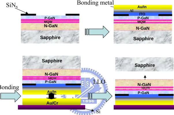
Figure 2.3 show the processing of the VLEDs. At first, the sample was deposited a 5000Å Si3N4 thin film layer on GaN-based LED film, followed by
photolithography patterning to define the isolation layer of device, then, the sputter evaporated ITO (300 nm) as the transparent contact layer, and fabricated reflective mirror which we evaporated Al (30nm) with electron-beam gum. About bonding metal was In/Au (30/150nm), and Si substrate was evaporated Cr/Au(30/1000nm). Finally, we bond sample and Si substrate at 350ºC and used laser lift-off technique to separate original sapphire substrate as shown in Figure 2.3. Then, the structure of VLEDs was finished
Reference
[2.1] S. Nakamura, M. Senoh, N. Iwasa, and S. Nagahama, Appl. Phys. Lett., 67 1868 (1995).
[2.2] S. Nakamura, M. Senoh, N. Iwasa, S. Nagahama, T. Yamada, T. Mukai, Jpn. J. Appl. Phys., 34 L1332 (1995).34 L1332 (1995).
[2.3] T. Mori, T. Kozawa, T. Ohwaki, Y. Taga, S. Nagai, S. Yamasaki, S. Asami, N. Shibata, and M. Koike,Appl. Phys. Lett., 69 3537 (1996).
[2.4] S. Strite, H. Morkoc, J. Vac. Sci. Technol. B10, 1237 (1992).
[2.5] S.A. Nikishin, N.N. Faleev, V.G. Antipov, S. Francoeur, L. Grave de Peralta, G.A. Seryogin, H. Temkin, T.I. Prokofyeva, M. Holtz, and S.N.G. Chu, Appl. Phys. Lett. 75, 2073 (1999).
[2.6] Chuong A. Tran, A. Osinski, R.F. Karlicek, Jr., I Berishev, Appl. Phys. Lett. 75, 1494 (1999).
[2.7] S. Sriram, G. Augustine, A. Burk, R. Glass, H. Hobogood, P. Orphanos, L. Rowland, T. Smith, C. Brandt, M. Driver, and R. Hopkins, IEEE Electron. Device Lett. 17, 369 (1996).
[2.8] D. L. Barton, M. Osinski, C. J. Helms, N. H. Berg, and B. S. Phillips, SPIE Int. Soc. Opt. Eng. 64 2694, (1996).
[2.9] M. K. Kelly, O. Ambacher, B. Dahlheimer, G. Groos, R. Dimitrov, H. Angerer, and M. Stutzmann, Appl. Phys. Lett. 69, 1749 (1996).
[2.10] A. Yasan, R. McClintock, K. Mayes, S. R. Darvish, H. Zhang, P. Kung, M. Razeghi, S. K. Lee and J. Y. Han, Appl. Phys. Lett. 81, 2151 (2002).
[2.11] T. Mori, T. Kozawa, T. Ohwaki, Y. Taga, S. Nagai, S. Yamasaki, S. Asama, N. Shibita, and M. Koite, Appl. Phys. Lett. 69, 3537 (1996).
L2112 (1989)
[2.13] X. Guo, and E. F. Schubert, Appl Phys. Lett. 78, 3337, (2001). [2.14] X. Guo, and E. F. Schubert, J. Appl Phys. 90, 4191, (2001).
[2.15] H. Kim, S. J. Park, H. Hwang, N. M. Park, Appl Phys. Lett. 81, 1326, (2002). [2.16] J. J. Wierer, D. A. Steigerwald, M. R. Krames, J. J. O’Shea, M. J. Ludowise, G.
Christenson, Y.-C. Shen, C. Lowery, P. S. Martin, S. Subramanya, W. Go¨ tz, N. F. Gardner, R. S. Kern, and S. A. Stockman., Appl. Phys. Lett. 78, 3379 (2001).
Sapphire substrate N-GaN N-Contact P-GaN MQW P-Contact Transparent contact
Figure2-1 The basic structure of GaN
Sapphire Polished GaN Ga+N2 GaN Epoxy Carrier substrate (Si) Workstation KrF Excimer Pulsed Laser Sapphire GaN Epoxy Carrier substrate (Si) Hot Plate heating Ga melting point=30℃
Figure2-2: The process scheme for fabrication of LLO un-ddoped GaN
Figure 2-3 The processing of vertical light emitting diodes MQW N-GaN P-GaN
LLO
Au/Cr SapphireSiN
xBonding metal
Bonding
Si Sapphire N-GaN MQW P-GaN Au/In Al ITO Sapphire N-GaN P-GaN MQW Sapphire N-GaN Au/In P-GaN MQWChapter 3
The progress of dry etching using by ICP-RIE
In this chapter, we report the progress of dry etching using by inductively coupled plasma reactive ion etching (ICP-RIE) for micro lens array and n-GaN surface roughening. The content consists of the introduction of photoresist, the re-flow of photoresist, the proportion of gases and the ICP bias for plasma etched. Finally, the images of etching result were taken by the scanning electron microscope (SEM).
3-1 Micro-lens formed by re-flow of photoresist
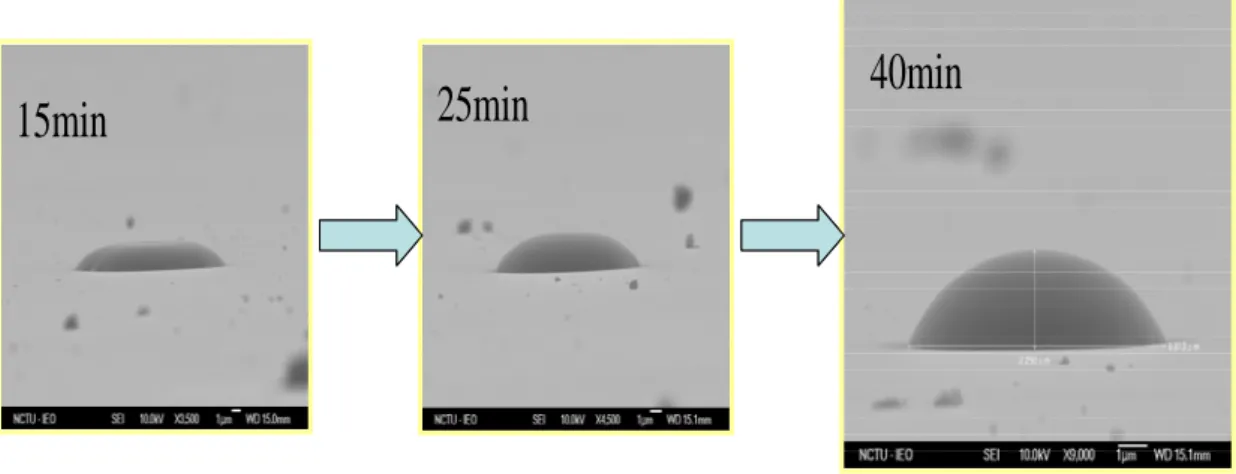
We use the well-known PR-reflow and dry-etching technique to fabricate n-GaN micro lens, and the basic method are well described in the literature.[3-1~3] The PR used in our experiments is AZ-5214E. An array of circular PR patterns with various diameter sizes is defined on an n-GaN film by the standard photolithography technique. The samples are then baked on hot plate, 168℃. The Si substrate transition temperature and PR start to flow. At the initial stage, the center was thinner and increased the circumference. As the temperature is further increased, the viscosity of the PR decreases, and the patterns eventually become convex with the center of each pattern the thickest. The smaller the diameter of the circular PR pattern, the lower the temperature required for convex shape formation. When the PR layer thickness and the baking temperature are 2.1um and 168℃, pattern diameter below 20um produce convex PR lens in a reproducible manner. Throughout the experiments the PR baking time is kept at 35min for consistency. Figure 3-1 shows the progress of micro lens formed by re-flow of photoresist.
15min
25min
40min
15min
25min
40min
Figure 3-1 The progress of micro lens formed by re-flow of photoresist
3-2 The etching result of micro lens array by ICP-RIE
At first, the micro-lens array with various diameter sizes was defined on an n-GaN film on sapphire by the standard photolithography and photoresist reflow technique. Then, the sample was etched by using ICP-RIE. The parameters we used is Cl2/Ar= 40/5 sccm, ICP power=550W, Bias=150W, 5mTorr. At this condition, the
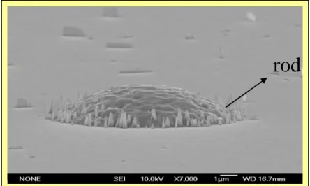
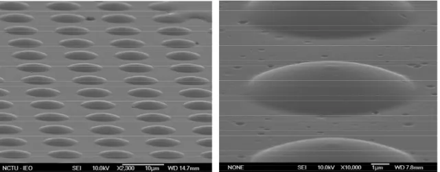
GaN etching rate was 330nm/min and the etching selectivity of GaN to photoresist was 0.58 for the n-GaN film that is on sapphire substrate. Figure 3-2 shows the SEM images of etching result, we can observe the planar and the micro lens, the planer is next to flat but the circumference of micro lens have the rod. In same condition, we also fabricated micro lens on laser lifted off n-GaN and etched by the same recipe as shown in Figure 3-3. It shows not only rods happened on the planar but also on the micro-lens. The planar also generated the rod and was not flat. The micro lens still had the rod. Therefore, we in order to improve the etching surface adjust the proportion of gas and the ICP bias for plasma etched.
rod
rod
Figure 3-2 The SEM images of etching result, the micro lens is fabricated on the basic structure
Micro lens
planar
Micro lens
planar
Figure 3-3 The SEM images of etching result, the micro lens is fabricated on vertical light emitting diode
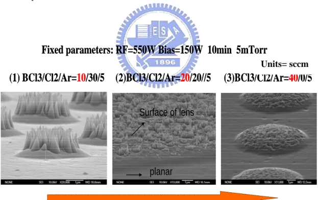
The main parameters of dry etching we discussed here are the mixture of gases and bias power.
Mixture of gases
etching surface roughness for III-nitride compounds. In this section, wed increased the ratio of BCl3 and Cl2 to understand the effect of the gases mixture on etching
surface. Figure3-4 shows the results under different ratio of BCl3 and Cl2. With
increasing the ratio, the surface roughness of micro-lens indeed becomes lower. However, the rod shape roughness always exists on the top of micro-lens in all these three conditions.
Bias power
In this experiment, we turned down the bias power to decrease the bombardment damage of photoreist. Figure3-5 shows the etching results under different bias power conditions. Obviously, the bombardment damage of photoreist could be eliminated as the bias power is lower than 75W.
Fixed parameters: RF=550W Bias=150W 10min 5mTorr
(1) BCl3/Cl2/Ar=
10
/3
0/5
(2)BCl3/Cl2/Ar=
20
/20//
5
(3)BCl3/Cl2/Ar=
40
/0/5
Fixed parameters: RF=550W Bias=150W 10min 5mTorr
(1) BCl3/Cl2/Ar=
10
/3
0/5
(2)BCl3/Cl2/Ar=
20
/20//
5
(3)BCl3/Cl2/Ar=
40
/0/5
Units= sccmSurface of lens
planar
Surface of lens
planar
Fixed parameters: BCl3/Ar=45/0 ICP=550W 5mTorr t=6min
(1) Bias=100W (2) Bias=75W (3) Bias=50W
Fixed parameters: BCl3/Ar=45/0 ICP=550W 5mTorr t=6min
(1) Bias=100W (2) Bias=75W (3) Bias=50W
Figure 3-5 As the bias decreasing, the SEM images of etching result
Finally, the dry etching was performed in a gas mixture of BCl3/Ar = 45 /0 sccm
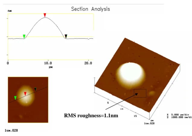
with an ICP source power of 550 W, a bias power of 50 W, etching time of 25min ,and a chamber pressure of 5 mTorr. At this condition, the GaN etching rate was 100nm/min and the etching selectivity of GaN to photoresist was 0.58. The etching was performed until the photoresist was etched away. Then, the GaN micro lens was formed on the LLO n-GaN surface. Figure 3-6 shows the final result of micro lens array on VLEDs. The AFM image was shown in Figure 3-7. The surface RMS is 1.1nm.
Figure 3-7 The AFM image of micro-lens RMS roughness=1.1nm
3-3 The progress of surface roughening for VLEDs
High power LED application is roughen the top surface of an LED is one of the methods for improving the light extraction. The roughening process was performed in an ICP-RIE. The parameters we used isCl2/Ar= 30/5 sccm, ICP power=550W,
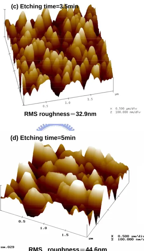
Bias=0W, 6mTorr. The n-GaN surface roughening was fabricated and the loss is not too much for n-GaN film. Figure 3-8 is an AFM image which shows the dry etching result at different etching time (conventional, 1min, 3.5min and 5min). The root mean square (RMS) roughness was obtained to be 1.2nm, 7.4nm, 32.9nm and 44.5 nm for conventional VLED, nano-roughened VLED with etching time of 1min, 3.5min and 5min, respectively. Obviously, the surface of VLED becomes more roughening as the etching time is longer. We could observe lots of granules were formed on sample
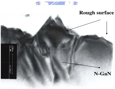
surface. In fact, the increase of roughness with the etching time increasing is because the size of the granules becomes larger. Using SEM, its size was found to be about 50nm, 150nm and 500nm at the etching time of 1min, 3.5min and 5min, respectively. Figure 3-9(a) shows the image of SEM for etching time=3.5min. Figure 3-9(b) is the image of SEM that compared surface before etching and after etching. In order to realize the cause of granules, we took the TEM photo as shown in Figure 3-10.In the figure, we could observe the dislocation exist in the bottom of those granules. This means the formation of granules could be partly attributed to the higher etching rate at the dislocation region generated than at other region. Of course, the relatively high etching rate of defects or those pits on LLO surface should be other possible reason to cause granules.
(a) Conventional RMS roughness=1.2nm (a) Conventional (a) Conventional RMS roughness=1.2nm 50nm RMS roughness=7.4nm (b) Etching time=1min 50nm RMS roughness=7.4nm (b) Etching time=1min
RMS roughness=32.9nm (c) Etching time=3.5min RMS roughness=32.9nm (c) Etching time=3.5min
RMS roughness=44.6nm
(d) Etching time=5min
RMS roughness=44.6nm
(d) Etching time=5min
Figure 3-8 AFM image of an N-face GaN surface etched by ICP-RIE (a)conventional devices (b)1-min etching (c) 3.5-min etching and (d) 5-min etching
no etching surface for n-GaN no etching surface for n-GaN
Figure 3-9 (a) shows the image of SEM for etching time=3.5min. (b) The image of SEM that compared surface before etching and after etching
N-GaN Rough surface
N-GaN Rough surface
Chapter4
Fabrication and Characteristics of GaN VLEDs with Micro Lens
Array
In this chapter, I demonstrate the fabrication and characteristics of GaN VLEDs with micro lens array. The size and coverage of micro lens on VLEDs, including of L-I-V、view angle were discussed. We compared our experiment data with the simulation results by Trace pro.
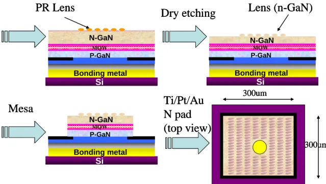
4-1 The Fabrication of GaN VLEDs with micro lens array
Figure 4.1 show the process of the GaN vertical light emitting diodes with micro-lens array. The process began with photolithography and photoresist reflow technique to form lens-shaped photoresist. AZ5214E photoresist was used and post baked. The detail of this process was discussed in 3-1. The photoresist lens was designed respectively, the photoresist lens was 3.5.10.15.20um and their height was 1.6-4.3um (see Table 4-1).Then, the dry etching was performed using on ICP-RIE with a gas mixture of BCl3/Ar = 45 /0 sccm, an ICP source power of 550 W, a bias
power of 50 W, and a chamber pressure of 5 mTorr. At this condition, the etching rate of GaN was 100nm/min and the etching selectivity of GaN to photoresist was 0.58. The etching was performed until the photoresist was etched away and measured using a scanning electronic microscope (SEM) The height of GaN lens is shown in Table (4-1). Figure 4.2 shows the SEM image of GaN micro-lens with diameter of 10 µm
The sample was deposited a 2um SiO2 film as etching mask and patterned by
photolithography technique to define the mesa region of device and followed by the dry etching process. The mesa region of device is 300μm × 300μm. Finally, the trilayers of Ti/Pt/Au (20 nm/20 nm/100 nm) served as n-type ohmic contact that was deposited by an e-gum.
The electrical characteristics of VLEDs with micro-lens array and conventional VLEDs were both measured by probe station system and evaluated by injecting different current density. The device is driven by Keithley 238CW current source, and its light output from top view could be observed by CCD. Current-voltage (I-V) measurements were performed using the probe station and the data could be fee-backed to the computer from these facilities by a GPIB card. Figure 4.3 shows the electrical measurement system. The light output power was measured using a calibrated power meter with a large Si detector (detector area 10×10 mm2) approximate 5 mm above the device, collecting the light emitted in the forward direction.
4.2 Characteristics of GaN VLEDs with micro lens array
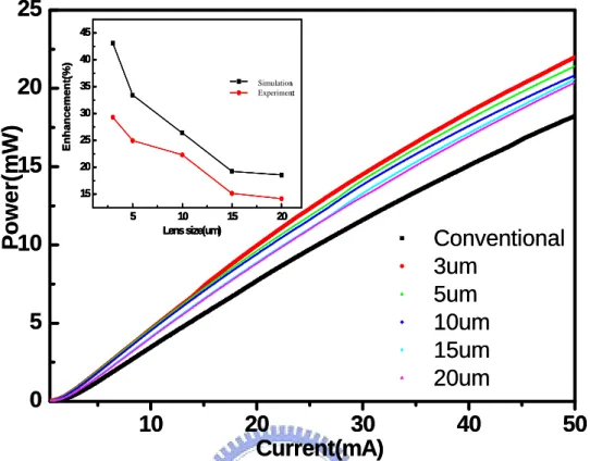
Figure 4.4 plots the current-voltage (I-V) characteristics of VLEDs with different size micro-lens (the space between micro-lens is kept to be 3um) and that of a conventional VLED fabricated on the same wafer. The forward voltage at 20mA (VF)
of conventional VLED and micro-lens VLEDs are almost the same (3.6V). The relation of light output power of our devices and driving current was plotted as shown in Figure 4.5. Figure4.6 shows the emission image of VLEDs with 3um lens array at inject on current of 0.5mA and 1.0mA. Compared to the conventional VLED, micro-lens VLEDs all show a stronger light output power. We plotter the enhancement of light output power of VLED with different size micro-lens at 20mA of driving current as shown in the inset.Clearly, the enhancement varies from 18% to 30% as the size of micro-lens varies from 20um to 3um. Especially, the enhancement shows a relatively rapid increase as the size of micro-lens is smaller than 15um. This phenomenon seems to suggest our variation of enhancement with micro-lens size is related to the curvature radius of micro-lens. In order to simply realize this
phenomenon, we considered the micro-lens is next to the part of sphere in reality and used equation r = ( h2
+a2)/(2h) to calculate curvature of the different size lens, where
‘r’ is the curvature , ‘h’ is the height of micro lens and ‘a’ is the radius of micro lens. We could obtained the curvature = 1.96, 3.27, 7.48, 12.53 and 22.18um for size of micro lens=3, 5, 10, 15 and 20um micro-lens, respectively. In our structure of VLEDs, the n-GaN film is 1.85um and MQW film is 0.05um. It is noticeable that the curvature center of 3um micro-lens is almost located at MQW considering the thickness of n-GaN and micro-lens. On the contrary, the curvature center of micro-lens rapidly far away MQW as the size of micro-lens is beyond 5um, especially beyond 15um. As shown inFigure4-11, the light cone for photon escaping outsider is the largest as the curvature center of micro –lens is located at MQW. This simply explains not only the largest enhancement of 3um micro-lens but also the small enhancement variation as the micro-lens size is larger than 15um. However, in order to clearly understand the actual effect of different micro-lens size on light output enhancement, we also need to consider the coverage of micro-lens. The coverage was defined as area of micro-lens/ total emitting area. We kept the total area of micro-lens array to be 1620×32×π (51% coverage) for VLEDs with different size micro-lens. The Figure 4.7 plots the L-I curve of conventional and micro-lens VLEDs and the enhancement of light output of micro-lens VLEDs. Similar to previous results, the light output power is also obviously enhanced as the size of micro-lens decreases. This again proves our explanation for the enhancement is reasonable. That is, the location of the curvature center of micro-lens determines the enhancement. However, compared with previous results, the enhancement of VLEDs with 5um, 10um, 15um, 20um lens was slightly lower. This should be due to less coverage of these size micro-lens compared with previous design. This also suggests the coverage of micro-lens array plays an important role for light extraction. The enhancement could be larger of we have
micro-lens array on VLEDs with larger coverage.
4.3 Simulation of GaN VLEDs with micro lens array
4-3.1 Simulation software – TracePro
TracePro is a comprehensive, versatile software tool for modeling the propagation of light in imaging and non-imaging opto-mechanical systems. TracePro is a Monte Carlo ray tracing program that accounts for flux or light power in your optical system, as well as the irradiance or the distribution of light. In Monte Carlo raytracing, scattering and diffraction are treated as random processes. Instead of propagating a distribution of light, discrete samples of the distribution, or rays, are propagated with BSDFs (Bidirectional Scattering Distribution Functions) used as probability distributions for determining ray directions. Monte Carlo ray tracing has several advantages over finite element methods. A list from includes
• Geometry can be procedural • No tessellation is necessary
• It is not necessary to precompute a representation for the solution • Geometry can be duplicated using instancing
• Any type of BRDF can be handled
• Specular reflections (on any shape) are easy • Memory consumption is low
• The accuracy is controlled at the pixel/image level
To use TracePro, you set up a model of your optical system within the program including optical and non-optical surfaces, and trace rays through the model.
4-3.2 Simulation of VLEDs with Micro Lens Array by Tracepro
We set up our structure in TracePro software. The size of device we simulated is 300μm×300μm. The structure contains a 1.85 µm-thick n-GaN; an active layer of five-period InGaN (2 nm)/GaN (8 nm) QWs; a 0.25 µm-thick p-GaN, and bonding metal located at bottom of structure with reflectivity of 80%. The micro lens array was set up following the real condition(Table 4-1). An absorbing box was placed very close to the device for simulating the intensity distribution of our devices. In this study, the propagation and reflection of light in the devices were examined by applying the ray tracing method in TracePro [4.1], [4.2]. The parameters used in all simulations of this work are shown in Table 4-2 and the emission power densities in the active regions of all devices were set identical in the simulation.
Figure 4-8 shows intensity distribution of GaN VLEDs with micro lens array simulated from the Trace Pro program. From the Figure4-9 we could see that the light intensity of GaN VLEDS with micro-lens is stronger than that of conventional VLED, especially, the region of micro-lens. This explains micro-lens could effectively enhance the probability for photons escaping outside VLED structure.
Figure 4.10 (a) and (b) show our simulation results and experimental data for comparison under the condition of fixed spacing (3um) and fixed coverage of micro-lens array, respectively. In both conditions, the experimental data is similar to the simulation results. That is, the enhancement increases as the lens size decreases. It also was a strong evidence to say that the enhancement of light output of our devices surely come from the micro-lens. However, some enhancement shift about 10% could be found between simulation and experimental data. This inaccuracy must comes from not perfect process (such as of bottom mirror during LLO procedure) or inaccurate parameters of simulation.
In summary, highly efficient GaN VLEDs with micro lens array were fabricated. Their characteristics were measured and compared with those of conventional VLEDs fabricated from the same wafer. The forward voltages at 20mA of conventional and micro-lens VLEDs were all around ~3.6V. As the size of micro-lens is 3um and the coverage is 51%, the light output of the micro-lens array VLEDs shows largest 30%. This result is also consistent with simulation.
Reference
[4.1] D. Eisert, and V. Harle, International Conference on numerical simulation of semiconductor optoelectronic devices, (2002).
[4.2] C. C. Kao, H. C. Kuo, H. W. Huang, J. T. Chu, Y. C. Peng, Y. L. Hsieh, C. Y. Luo, and S. C. Wang, C. C. Yu, C. F. Lin, IEEE Photonics Technology Lett. 17, 19 (2005).
Figure 4.1 the processing of the GaN vertical light emitting diodes with micro-lens array
Dry etching
Mesa
Ti/Pt/Au
N pad
(top view)
Lens (n-GaN)
300um 300um MQW N-GaN P-GaNPR Lens
Bonding metal Si MQW N-GaN P-GaN Bonding metal Si MQW N-GaN P-GaN Bonding metal SiFigure 4.1 the processing of the GaN vertical light emitting diodes with micro-lens array
Dry etching
Mesa
Ti/Pt/Au
N pad
(top view)
Lens (n-GaN)
300um 300um MQW N-GaN P-GaNPR Lens
Bonding metal Si MQW N-GaN P-GaN Bonding metal Si MQW N-GaN P-GaN Bonding metal SiDry etching
Mesa
Ti/Pt/Au
N pad
(top view)
Lens (n-GaN)
300um 300um MQW N-GaN P-GaN MQW N-GaN P-GaNPR Lens
Bonding metal Si MQW N-GaN P-GaN Bonding metal Si MQW N-GaN P-GaN Bonding metal Si MQW N-GaN P-GaN Bonding metal Si MQW N-GaN P-GaN Bonding metal SiFigure 4.2 the SEM image of the GaN micro-lens array Figure 4.2 the SEM image of the GaN micro-lens array
CCD Objective Keithley 238 driver Power supply Power meter Spectrum analyzer Computer Integrating sphere PD Prober CCD Objective Keithley 238 driver Power supply Power meter Spectrum analyzer Computer Integrating sphere PD Prober CCD Objective Keithley 238 driver Keithley 238 driver Power supply Power supply Power meter Power meter Spectrum analyzer Spectrum analyzer Computer Computer Integrating sphere PD Prober
Figure4-3 The probe-station system is used for electronically characteristic measurements
0
1
2
3
4
5
6
Figure4-4 Curves of current-voltage (I-V) of VLEDs with micro lens array and a conventional VLED fabricated from the same wafer.
0
5
10
15
20
25
30
35
40
45
Conventional 3um 5um 10um 15um 20umCurrent(mA)
Voltage(v)
0
5
10
15
20
25
Figure4-5 Light output power of VLEDs with micro lens array and a conventional LED as functions of injected current density. The insert shows the enhancement-lens size curves.
Figure4-6 the VLEDs with 3um lens array have injected 0.5 mA and 1.0 mA .
0.5mA 3um Lens 1mA 3um Lens
GaN micro lens GaN micro lens
0.5mA 3um Lens 1mA 3um Lens
0.5mA 3um Lens
0.5mA 3um Lens 1mA 3um Lens1mA 3um Lens
GaN micro lens GaN micro lens
0
10
20
30
40
50
Conventional 3um 5um 10um 15um 20umCurrent(mA)
Po
wer
(mW)
5 10 15 200
5
10
15
20
25
5 10 15 20 25 30 2000/45 Lens size(um) En han c emen t( %)0
10
20
30
40
50
Conventional 3um 5um 10um 15um 20umCurrent(mA)
Po
wer
(mW)
5 10 15 200
5
10
15
20
25
5 10 15 20 25 30 2000/45 Lens size(um) En han c emen t( %)0
10
20
30
40
50
Conventional 3um 5um 10um 15um 20umCurrent(mA)
Po
wer
(mW)
5 10 15 20 5 10 15 20 25 30 2000/45 Lens size(um) En han c emen t( %)0
5
10
15
20
25
Figure 4-7 The same coverage for the different size lens. Light output power of VLEDs with micro lens array and a conventional LED as functions of injected current density. The insert shows the enhancement-lens size curves.
(units:um)
pad
Boning metal (80% reflection) MQW P-GaN N-GaN 1.85 0.25 0.05 detector (100% absorption) 1mw 1mW (units:um) pad
Boning metal (80% reflection) MQW P-GaN N-GaN 1.85 0.25 0.05 detector (100% absorption) 1mw 1mW
Figure 4-8 an irradiance map of GaN VLEDs with micro lens array of 300×300 µm2 simulated from the Trace Pro program
Experiment
10
20
30
40
50
Conventional
3um
5um
10um
15um
20um
Current(mA)
Po
w
e
r(
mW
)
5 10 15 200
5
10
15
20
25
15 20 25 30 35 40 45 Simulation Same area Lens size(um) E n h ancem en t(%) Simulation Experiment10
20
30
40
50
Conventional
3um
5um
10um
15um
20um
Current(mA)
Po
w
e
r(
mW
)
5 10 15 20 15 20 25 30 35 40 45 Simulation Same area Lens size(um) E n h ancem en t(%) Simulation Experiment 5 10 15 20 15 20 25 30 35 40 45 Simulation Same area Lens size(um) E n h ancem en t(%) 5 10 15 20 15 20 25 30 35 40 45 Simulation Same area Lens size(um) E n h ancem en t(%) Simulation ExperimentConventional 5um lens
Conventional 5um lens
Conventional 5um lens
Figure 4-9 Light intensity distributed from the surface of detector box that is most next to the top surface of device by Trace Pro.
Figure4-10 (a) the experiment that fixed the space with different size of micro lens compared with simulation results. (b) the experiment that same coverage of micro lens compared with simulation results.
0 5 10 15 20 0 10 20 30 40 50 Simulation sample A (2000/45) Lens size(um) hancem t(%) 5 10 15 20 En en 15 20 25 30 35 40 45 Simulation Same area Lens size(um) En han c emen t(%) Simulation Experiment Simulation Experiment 0 5 10 15 20 0 10 20 30 40 50 Simulation sample A (2000/45) Lens size(um) hancem t(%) 5 10 15 20 15 20 25 30 35 40 45 En
en Simulation Same area
Lens size(um) En han c emen t(%) Simulation Experiment Simulation Experiment
pad
MQW
P-GaN
N-GaN
1.85
0.25
0.05
Units :um)
Figure 4-11 the light cone for photon escaping outsider is the largest as the curvature center of micro –lens is located at MQW
H L
Refractive index (n) Reflection of Bonding metal (80%) n-GaN 2.5 Total power from
p-GaN 2.5 the active region (mW) 2 Air 1 Absorption coefficient 100 MQW 2.5 (λ = 460 nm, cm-1) 4.30/2.38 2.12 1.92 1.16 /0.71
Lens height (after etching) 1.61 1.99/ 3.36/ 3.81/
ens height (PR)/ units (um) 20um 15um 10um 5um 3um Lens size ard bake (168°C) Time (45min) 4.30 3.81/ 3.36/ 1.99/ 1.61 ens height (PR)/ units (um) 20um 15um 10um 5um 3um Lens size ard bake (168°C) Time (45min) H
L Lens height (after etching) /0.71 1.16 1.92 2.12 /2.38
Table 4-1 The height of different size of micro lens
Table 4-2 Parameters for the light-tracing simulation of VLED with micro lens array
Chapter5
Fabrication and characteristic of GaN VLEDs with surface
roughening
In this chapter, I demonstrate the fabrication of GaN VLEDs with surface roughening, and we will discuss the scanning electron micrographs (SEM) image, the atomic force microscopy (AFM) image, the transmission electron microscopy (TEM) image of N-GaN surface roughening and performances of devices.
5-1 The Fabrication of GaN VLEDs with surface roughening
Figure 5-1 shows the process of the GaN vertical light emitting diodes with surface roughening which began 2-4 “the structure of vertical light emitting diodes”. At first, because of some treatments such as dry etching for roughening surfaces might cause electrical deterioration , we protected the surface of pad and passivation, the sample was deposited a 0.5um SiNx thin film layer on GaN-based VLED film and
followed by photolithography patterning. For n-GaN surface roughening formation, a dry etching method by inductively coupled plasma (ICP) self-aligned dry etching (Samco ICP-RIE). The dry etching was performed in a gas mixture of Cl2/Ar = 30 /5
sccm with an ICP source power of 500 W, a bias power of 0 W, and a chamber pressure of 6 mTorr. The roughenss could be controlled by the etching time. In our experiment, we have three etching times: 1min, 3.5min and 5min for different devices. The result of etching described detailedly in chapter3.
Then, the sample was deposited a 2um SiO2 film as etching mask and followed
by photolithography patterning to define the mesa region of device, and dry etched the mesa of device (300μm × 300μm), Finally, the trilayers of Ti/Pt/Au (20 nm/20 nm/100 nm) for n-type ohmic contact were deposited by an e-gum. The diameter for circle n-type ohmic contact is 100μm, the n-GaN film is 3.85um and MQW film is 0.05um
in our device. The conventional VLEDs with the same mesa size (300 µm × 300 µm) were also fabricated from the same wafer for comparison. Figure 5-2(a) shows plan-view microphotographs of an VLED bonded on a Si substrate before roughening the surface and after roughening the surface is shown in Figure 5-2(b).
The electrical characteristics of VLEDs with surface roughening and conventional VLEDs were both measured by probe station system and evaluated by injecting different current density. The device is driven by Keithley 238CW current source, and its light output from top view could be observed by CCD. Current-voltage (I-V) measurements were performed using the probe station and the data could be fee-backed to the computer from these facilities by a GPIB card. The light output power was measured using a calibrated power meter with a large Si detector (detector area 10×10 mm2) approximate 5 mm above the device, collecting the light emitted in the forward direction.
5-2 Characteristics of GaN VLEDs with surface roughening
Figure 5-3 plots the current-voltage (I-V) characteristics with different etching times for the surface roughening LLO GaN VLED devices. All I-V curves showed linear characteristics up to 50mA. Because of the higher thermal conductivity of Si compared sapphire, these devices are advantageous for high-power operation. The forward voltage at 20mA, VF = 4.44, 4.43, 4.53 and 4.55V for conventional VLED,
nano-roughened with1-min-etched, 3.5-min-etched and 5-min-etched, respectively. In this data, we could understand roughening surfaces might cause electrical deterioration in our case.
As shown in Figure 5-4, the output power from the surface of the chip versus dc injection current (L-I) characteristics for the VLEDs with different etching times. All L-I curves showed linear characteristics up to 50mA. The output power at a given
current increased with increasing etching time. As compared with the output power for a flat-surface VLED and the 10-min-etched surface VLED, the roughening treatment resulted in an increase of output power by a factor of 2.1 from the top surface. From other measurements on different etching time devices, the power also showed to enhance 30% and 95%. This output power measurement was performed from the upper side of the chip using a Si photodiode. It means that the power measurement is a relative output measurement from the top surface of the chip. Figure5-5 shows the VLEDs with surface roughening and conventional VLEDs at the same injected current 1mA, we could observe the relative intensity about output power.
In summary of the chapter, an etching method has been applied to a GaN-based VLED for the purpose of increasing extraction efficiency. VLED output test results have indicated that, presumably due to the decrease in light propagation in GaN film, there is a relationship between a roughened appearance and extraction efficiency. Although total integrated optical power has not been measured, the extraction efficiency from a top surface was increased 30% to 110% compared to that of a conventional VLED and the electrical properties of devices were similar. It is notable that the technique mentioned in this chapter is simple and does not require complicated processes, implying that it will be suitable for manufacturing of GaN-based VLEDs with surface roughening.
Units :um Si
ICP etching
Ti/Pt/Au
N pad
(top view)
300um 100um Cl2/Ar=30/5sccm 6Pa ICP/Bias=500/0WEtch mask SiO2 3000Å
MQW N-GaN P-GaN Bonding metal 300um MQW N-GaN P-GaN Bonding metal MQW N-GaN P-GaN Bonding metal Si
Mesa
3.5 0.05 0.25 300um Si Si Units :um SiICP etching
Ti/Pt/Au
N pad
(top view)
300um 100um Cl2/Ar=30/5sccm 6Pa ICP/Bias=500/0WEtch mask SiO2 3000Å
MQW N-GaN P-GaN Bonding metal 300um MQW N-GaN P-GaN Bonding metal MQW N-GaN P-GaN Bonding metal Si
Mesa
3.5 0.05 0.25 300um Si SiICP etching
Ti/Pt/Au
N pad
(top view)
300um 100um Cl2/Ar=30/5sccm 6Pa ICP/Bias=500/0WEtch mask SiO2 3000Å
MQW N-GaN P-GaN Bonding metal 300um MQW N-GaN P-GaN Bonding metal MQW N-GaN P-GaN Bonding metal Si
Mesa
3.5 0.05 0.25 300um SiICP etching
Ti/Pt/Au
N pad
(top view)
300um 100um Cl2/Ar=30/5sccm 6Pa ICP/Bias=500/0WEtch mask SiO2 3000Å
MQW N-GaN P-GaN Bonding metal 300um MQW N-GaN P-GaN Bonding metal MQW N-GaN P-GaN Bonding metal Si
Mesa
3.5 0.05 0.25 300umICP etching
Ti/Pt/Au
N pad
(top view)
300um 100um Cl2/Ar=30/5sccm 6Pa ICP/Bias=500/0WEtch mask SiO2 3000Å
MQW N-GaN P-GaN MQW N-GaN P-GaN Bonding metal 300um MQW N-GaN P-GaN 300um MQW N-GaN P-GaN MQW N-GaN P-GaN Bonding metal MQW N-GaN P-GaN Bonding metal Si
Mesa
3.5 0.05 0.25 MQW N-GaN P-GaN Bonding metal Si MQW N-GaN P-GaN Bonding metal SiMesa
3.5 0.05 0.25 300um Si SiFigure 5-1 the processing of the GaN vertical light emitting diodes with surface roughening
Figure 5-1 the processing of the GaN vertical light emitting diodes with surface roughening