國 立 交 通 大 學
電信工程學系
博 士 論 文
小型之寬頻一百八十度混合式耦合器及其
應用於寬頻耦合器與濾波器之設計
A Compact Wideband 180
0
Hybrid Coupler
and Its Applications to Wideband Coupler and
Bandpass Filter Designs
研究生:紀鈞翔 (Chun-Hsiang Chi)
指導教授:張志揚 (Chi-Yang Chang)
小型之寬頻一百八十度混合式耦合器及其應用於
寬頻耦合器與濾波器之設計
A Compact Wideband 180
o
Hybrid Coupler and Its
Applications to Wideband Coupler and Bandpass
Filter Designs
研究生:紀鈞翔
Student:
Chun-Hsiang
Chi
指導教授:張志揚 博士 Advisor:
Dr.
Chi-Yang
Chang
國立交通大學
電信工程學系
博士論文
A Dissertation
Submitted to Institute of Communication Engineering
College of Electrical and Computer Engineering
National Chiao Tung University
in Partial Fulfillment of the Requirements
for the Degree of Doctor of Philosophy
in
Communication Engineering
Hsinchu, Taiwan
小型之寬頻一百八十度混合式耦合器及其
應用於寬頻耦合器與濾波器之設計
研究生:紀鈞翔 指導教授:張志揚博士
國立交通大學
電信工程學系
摘要
本論文主要研究小型之寬頻一百八十度混合式耦合器以及其應
用,在第一部份,介紹步階式寬頻一百八十度混合式環形耦合器,其
新型的寬頻一百八十度相位移相器以混合共平面帶線/指插式共平面
帶線來實現,由於結合步階阻抗架構及寬頻的相位反轉器,此提出的
混合式耦合器不僅尺寸小、寬頻且擁有卓越的性能,在第二部分,提
出利用垂直安置基板耦合器的寬頻多節式一百八十度混合式耦合
器,基於變形的理想單節式混合式耦合器(內含理想相位反轉器的一
百八十度混合式耦合器),多節的一百八十度混合式耦合器可藉由適
當的串接單節的混合式耦合器來實現,相較於傳統的二分之三波長岔
路環,此兩節式的混合式耦合器頻寬寬、尺寸小且容易達到高比例的
能量分流。最後,介紹藉由串接兩個步階式一百八十度混合式耦合器
來實現擁有寬的上止帶之寬頻帶通濾波器。上述電路的分析過程皆有
詳細的說明,也提供設計方程式及設計曲線,因此,我們可以系統化
的設計這些電路。
A Compact Wideband 180
o
Hybrid Coupler
and Its Applications to Wideband Coupler
and Bandpass Filter Designs
Student:Chun-Hsiang Chi Advisor:Dr. Chi-Yang Chang
Department of Communication Engineering
National Chiao Tung University
Abstract
This dissertation presents the research and application of the compact wideband 1800 hybrid coupler. In the first part, a stepped-impedance wideband 1800 hybrid ring
coupler with a novel wideband 1800 phase-shifter implemented by the hybrid CPS/interdigital CPS structure is introduced. Due to the combination of the
stepped-impedance structure and a wideband phase inverter, the proposed hybrid coupler achieves size reduction, wide bandwidth, and excellent phase and amplitude performances. In the second part, wideband multi-section 1800 hybrid couplers using
the vertically installed planar (VIP) coupler are proposed. On the basis of the reconfigured ideal single-section 1800 hybrid coupler (the 1800 hybrid coupler with an
ideal phase inverter), the multi-section 1800 hybrid rings can be realized by properly cascading of the single-section 1800 hybrid coupler. Compared to the conventional 3/2 λ 1800
hybrid ring, the two-section hybrid rings exhibit wide bandwidth, size reduction, and easily achievable high power-division ratios. Finally, a wideband bandpass filter with wide upper stopband is presented by cascading two
stepped-impedance 1800 hybrid couplers. Analysis procedures of above-mentioned circuits are described in detail. Also, design equations and design curves are presented. Therefore, we can systematically design these circuits.
誌謝
感謝張志揚教授這些年來在研究上給予的指導與啟發,使得本研
究得以完成,教授豁達開朗、平易近人的個性,更拉近師生之間的距
離,再者,教授見識廣闊,與教授聊天,不僅輕鬆愉快,亦獲益良多,
讓研究生活增添另一番樂趣。另外,亦感謝口試委員陳俊雄教授、鍾
世忠教授、郭仁財教授、邱煥凱教授、江逸群教授與湯敬文教授對本
研究給予的建議與指正。
在此亦特別感謝實驗室的學長、弟、妹的照顧,特別是王士鳴、
謝明諭、李建育,除了研究上的討論外,生活的經驗談以及抒解壓力
的活動都給予不少的幫助,另外,更要感謝吳中宏,常常找我泡溫泉
以及開車載我去兜風,空閒的時候找我閒話家常,使得研究生活更多
采多姿。
最後,在此感謝家人以及女友在背後默默地給予支持與鼓勵,讓
我無後顧之憂的完成學業。
鈞翔
2009 年 1 月於新竹
Contents
Abstract (Chinese)………..………..Ⅰ Abstract...…………...………..……….Ⅱ Acknowledgement………Ⅲ Contents………Ⅳ List of Tables……..………...………...……Ⅵ List of Figures……….….…………...………...…...………...Ⅶ 1 Introduction………...………..……….….….1 1.1 Research motivations………...………2 1.2 Literature survey………..………3 1.3 Contribution……….51.4 Organization of the dissertation………..5
2 A Compact Wideband 1800 Hybrid Coupler Using a Novel Interdigital CPS Phase Inverter……….………...….………....7
2.1 Analysis of stepped-impedance line section….………...…9
2.2 Design steps of proposed 1800 hybrid ring coupler………...10
2.3 Realization and measurement………...…….….11
3 Wideband Multi-section 1800 Hybrid Couplers Using Vertically Installed Planar Couplers………..……...……….……..…….19
3.1 Theoretical analysis of the two-section hybrid ring………...….22
3.2 Characteristics of VIP couplers……..………..…………...……...….29
3.3 Experimental results and discussion……….………...…...…...…..31
4 Wideband Bandpass Filters with Wide Upper Stopband Using Stepped- Impedance Rat-Race Hybrid Couplers..………..…………...40
4.1 Bandpass filter by cascading two 1800 hybrid couplers………….…………41
4.2 bandpass filter by cascading two stepped-impedance 1800 hybrid couplers with one unit element……….…………45
two unit elements……….…..51
5 Conclusion……..………..……….………..58
List of Tables
Table 2.1 Parameters of the stepped-impedance hybrid ring………...……....10
Table 2.2 CPS and interdigital CPS parameters of the stepped-impedance hybrid ring………....………..…12
Table 2.3 Summary of measured performances of the 1800 hybrid ring coupler...18
Table 3.1 VIP coupler parameters extracted by HFSS (f0=2 GHz)………...…..30
Table 4.1 Parameters of the stepped-impedance bandpass filter………. 49
Table 4.2 Computed results by HFSS (f0=2 GHz)………..….…49
Table 4.3 Parameters of the stepped-impedance bandpass filter………...…….. 54
Table 4.4 CPS and Interdigital CPS parameters of the stepped-impedance bandpass filter………...….. 54
List of Figures
Figure 1-1 Schematic of the conventional rat-race hybrid.………...…….…2
Figure 1-2 Schematic of the 1800 hybrid ring coupler proposed by March ..…………3 Figure 2-1 Configuration of the wideband phase inverter realized with CPS...……….8
Figure 2-2 Schematic of the 1800 hybrid ring with an ideal 1800 phase inverter….…..8
Figure 2-3 Proposed configurations of the stepped-impedance 1800 hybrid ring coupler using interdigital CPS (a) λ/4 line section (b)λ/4 line section with a wideband phase inverter……...…………...………..8 Figure 2-4 (a) Quarter-wave transmission line (b) Stepped-impedance circuit equivalent to a quarter-wave transmission line…….………...……9
Figure 2-5 Cross-sectional view of the interdigital CPS with N=3………...……...…11
Figure 2-6 Computed characteristic impedance and effective dielectric constant of
CPS as a function of the gap width with the strip width as a parameter, t=0 mil…..……….……….……….….12
Figure 2-7 Computed characteristic impedance and effective dielectric constant of
interdigital CPS as a function of the gap width with the number of CPS strip pair as a parameter, t=0 mil (a) w=3 mil (b) w=4 mil…….……....13
Figure 2-8 Simulated magnitude of S11 and S21 and insertion phase difference between
t w o c o n f i g u r a t i o n s o f F i g . 2 ( a ) a n d ( b ) w i t h ZH= 1 8 4Ω, θH=15.20,ZL=22Ω and θL=16.30 where the S-parameters are based on 50-Ω port impedances……….14 Figure 2-9 Fabricated 1800 hybrid ring coupler (a) Layout (b) Photograph.……...…15
Figure 2-10 Measured results of the fabricated 1800 hybrid ring coupler (a) Out-of- phase operation (b) In-phase operation..…………..…...………16
Figure 2-11 Measured phase and amplitude differences of the fabricated 1800 hybrid
ring coupler (a) Out-of-phase operation (b) In-phase operation.…...…17
Figure 2-12 Measured and simulated results from 0 to 20 GHz.……….18
hybrid ring (b) Reconfigured hybrid ring (c) Proposed two-section hybrid
ring.……….……….…..21 Figure 3-2 Schematic of the proposed two-section hybrid ring with a unit element at each I/O port.………..………..….……..……...21
Figure 3-3 Even-mode and (b) odd-mode equivalent circuits of the rat-race ring coupler using an ideal phase inverter.………...………...21
Figure 3-4 Characteristic impedances Z1, Z2, and bandwidth versus return loss for the equal-ripple response 3-dB two-section hybrid ring.………...…………..25 Figure 3-5 Characteristic impedances Z1, Z2, and bandwidth versus coupling level for
the single- and two-section hybrid rings with 15-dB equal-ripple return loss.………..………...…26
Figure 3-6 Another set of characteristic impedances Z1, Z2, and bandwidth versus coupling level for the two-section hybrid rings with 15-dB equal-ripple return loss.………..……...……….27
Figure 3-7 Characteristic impedances Z1, Z2, Z3, Z4, and bandwidth versus return loss for the equal-ripple response 3-dB two-section hybrid ring with a unit
element at each I/O port. ………...………28 Figure 3-8 Cross-sectional view of the VIP coupler.….……….………..28 Figure 3-9 Equivalent circuit of a short-ended coupled line………....30
Figure 3-10 Simulated 15-dB equal-ripple return loss bandwidth of a 3-dB single- section hybrid ring with a short-ended coupler versus different
Z0e.………..………..……...31
Figure 3-11 3-D structure of the single-section hybrid ring using the VIP coupler.………...……….………..……..32
Figure 3-12 Fabricated circuits of the conventional and reconfigured single-section hybrid rings.……….…..………33
Figure 3-13 Fabricated two-section hybrid rings (a) 3-dB hybrid ring (b) 20-dB hybrid ring (c) 3-dB hybrid ring with a unit element at each I/O port.………...34 Figure 3-14 Measured and simulated results of the 3-dB two-section hybrid ring (a)
Out-of-phase operation (b) In-phase operation.…….…...35 Figure 3-15 Measured amplitude and phase imbalances of the 3-dB two-section
Figure 3-16 Measured and simulated results of the 20-dB two-section hybrid ring....37
Figure 3-17 Measured and simulated results of the 3-dB two-section hybrid ring with a unit element at each I/O port (a) Out-of-phase operation (b) In-phase operation……….38
Figure 3-18 Measured amplitude and phase imbalances of the 3-dB two-section hybrid ring with a unit element at each I/O port (a) Out-of-phase operation
(b) In-phase operation………39 Figure 4-1 Schematic of the proposed wideband bandpass filter using two 1800 hybrid ring couplers.……….……….…………..…….….……41
Figure 4-2 Characteristic impedances Z1 and Z2 versus bandwidth for the wideband bandpass filter with 15-dB equal-ripple return loss.………..….…..…….42
Figure 4-3 Characteristic impedances Z1 and Z2 versus bandwidth for the wideband bandpass filter with 20-dB equal-ripple return loss……….………..43 Figure 4-4 Circuit configuration of the realized phase inverter and crossover..……..43
Figure 4-5 Photograph of the fabricated filter………...44 Figure 4-6 Measured and simulated results of the wideband bandpass filter………..45
Figure 4-7 Schematics of the proposed wideband filters (a) Basic structure (b) Modified structure……….……….45 Figure 4-8 Characteristic impedances Z1, Z3, and bandwidth versus return loss for the
equal-ripple response bandpass filter shown in Fig. 4-7(b).……....……..46 Figure 4-9 Simulated results of the proposed wideband filter (a) Basic structure (b)
Modified structure.………...……..…47 Figure 4-10 Geometry of the fabricated filter (a) Main circuit section. W1=101 mil, W2=12 mil, W3=135 mil, W4=17 mil, S=82 mil, L1=158 mil, L2=283 mil,
L3=200 mil, L4=195 mil, L5=201 mil (b) VIP stepped-impedance coupler. Wv1=133 mil, Wv2=29 mil, Lv1=184 mil, Lv2=296 mil.………..………...49
Figure 4-11 (a) 3-D structure of the proposed wideband filter with the stepped- impedance structure (b) Photograph of the fabricated filter…………....50 Figure 4-12 Measured and simulated results of the proposed wideband filter with the
stepped-impedance structure.……….……….……...51 Figure 4-13 Schematics of the proposed wideband bandpass filters with no crossover (a) Basic structure (b) Modified structure.……….………....……..52
Figure 4-14 Characteristic impedances Z1, Z3, and bandwidth versus return loss for
the equal-ripple response bandpass filter shown in Fig. 4-13(b).……..…53 Figure 4-15 Layout of the fabricated stepped-impedance wideband bandpass
filter.………...……….……54 Figure 4-16 Layouts of discontinuities (a) Discontinuity A (b) Discontinuity B (c)
Discontinuity C (d) Discontinuity D (e) Discontinuity E…….……….…55 Figure 4-17 Simulated results of the proposed stepped-impedance wideband bandpass
filter by using the circuit simulator………56 Figure 4-18 EM simulated results and measured results of the proposed bandpass
filter.……...………56 Figure 4-19 Photograph of the fabricated stepped-impedance wideband bandpass
Chapter 1
Introduction
The 1800 hybrid ring coupler is a fundamental component in microwave circuit applications. Conventionally, a rat-race hybrid consists of three λ/4 line sections and a 3λ/4 line section as shown in Fig. 1-1. A signal applied to port 1 will be split into two in-phase signal at ports 3 and 4, and port 2 will be isolated. A signal applied to port 2 will be split into two out-of-phase signal at ports 3 and 4, and port 1 will be isolated.
It can be used as an 1800-out-of-phase or in-phase power divider with isolated output ports. Due to these characteristics, the 1800 hybrid coupler is widely used in balanced mixers, push-pull amplifiers, phase shifters, and feeding networks of antenna arrays.
Recently, a wideband bandpass filter is an important issue in the development of the wideband communication systems. In the design of the wideband filter, two major
issues must be considered. One is the wide bandwidth; the other is the spurious problem. In wideband applications, the filter needs not only wide bandwidth to meet the required large data rate but also wide stopband to suppress harmonics.
In this chapter, we describe the shortcomings of the conventional rat-race hybrid, the challenges in the design of the wideband bandpass filter, previous works for
Fig. 1-1. Schematic of the conventional rat-race hybrid.
1.1 Research Motivations
In the conventional rat-race hybrid, the 1800 phase shifter is implemented by a λ/2 transmission line and its phase-shift is only 1800 at the center frequency. Therefore, the conventional hybrid ring using a 3λ/4 line section results in large size and narrow bandwidth. Besides, it requires a quite high impedance line for large power-division ratios.
A wideband bandpass filter with the traditional microstrip half-wavelength parallel
coupled-line structure is difficult to manufacture due to very small gaps between coupled strips. Moreover, because of the unequal even- and odd-mode phase
velocities, this filter has a first spurious passband at twice of the midband frequency, resulting in poor harmonic suppression.
Most of the proposed circuits are implemented on microstrip structures because
microstrip is the most mature and widely used transmission line. However, the realization of a broadband phase inverter using microstrip structure would be a
challenge. In recent years, due to advantages of small dispersion, simple realization of short-circuited ends, easy integration with lumped elements and no need for via holes, uniplanar transmission lines such as coplanar waveguide (CPW) and coplanar strip
(CPS) have become a competitive alternative to microstrip in many applications. Therefore, the purpose of this research is to find some approaches to overcome
bandwidth and size problems of the rat-race hybrid on microstrip and uniplanar structure. Furthermore, based on theses proposed 1800 hybrid couplers, several novel
bandpass structures are proposed to solve bandwidth and harmonics problems.
Fig. 1-2. Schematic of the 1800 hybrid ring coupler proposed by March.
1.2 Literature Survey
In the design of the 1800 hybrid coupler, many approaches [1]-[5] have been
proposed to achieve small size. In [1], [2], using lumped elements were proposed to reduce the size of the hybrid. In [3], a design method for 1.25λ-and 7λ/6-ring 3-dB hybrids using λ/8 and λ/6 section was proposed. Other miniaturized methods were also presented such as folded line [4] and artificial lines [5]. However, in all above-mentioned 1800 hybrids, it is difficult to simultaneously achieve small size and wide bandwidth. March [6] replaced the 3λ/4 transmission line with an opposing ends short-circuited λ/4 coupled line to increase the bandwidth of the hybrid ring as shown in Fig. 1-2. However, to implement this hybrid ring requires extremely tight coupled lines. A reduced-size rat-race coupler of length 19λ/18 has been developed in [7]. In [8], a lumped-element left-handed transmission line was used to realize the hybrid ring. The 3λ/4 section of the rat-race has been replaced with a λ/4 section and various forms of wideband phase inverters [9]-[16].
A theory of cascading of several quarter-wave transmission-line sections to each
I/O port of an ideal 1800 hybrid ring for bandwidth improvement has been proposed by Rehnmark [17]. Chang et al. [18] have proposed a method to implement the hybrid
ring proposed in [17]. However, to implement these hybrid rings requires extremely
low and/or high impedance lines or extremely tight coupled lines especially for large power-division ratio situations. To reduce the impedance values, the 3λ/4 line section of the hybrid ring can be split into three λ/4 lines [19]. However, the required high impedance values still increase with power-division ratios. Therefore, the realizable highest and/or lowest impedance values limit the achievable power-division ratios of
those hybrid rings proposed in [1]-[19].
The 900 branch-line coupler [20] realized with a multi-section structure for bandwidth enhancement is well known. The multi-section 1800 hybrid ring was first
proposed by Ang et al. [21] to achieve broad bandwidth and high power-division ratios. However, because each single-section unit in [21] was based on the
conventional hybrid ring coupler with the narrow-band phase inverter, the amplitude and the phase performances of two output ports cannot achieve broad bandwidth simultaneously. Therefore, in [21], only conditions at the center frequency are derived
and the responses other than center frequency have not been discussed analytically. In addition, the bandwidth of the hybrid ring will dramatically decrease with increasing
of power-division ratios.
In the design of the wideband bandpass filter, based on the insertion loss method [22], a wideband bandpass filter function of Chebyshev type can be easily synthesized.
However, to realize a wideband bandpass filter with the conventional microstrip half-wavelength parallel coupled-line structure, very small gaps between coupled
strips are required to achieve a tight coupling. This may cause some difficulties in the fabrication processes. Moreover, due to the unequal even- and odd-mode phase velocities, this filter has a first spurious passband at 2f0, resulting in poor harmonic
suppression. To improve bandwidth performance, several methods [23]-[34] have been proposed. In [23], a bandpass filter with increased bandwidth can be obtained
from resonator coupling enhancement with the three-line coupling structure was reported. Another method for coupling enhancement using apertures etched in the microstrip ground plane was described in [24]. In [25], a cascade of two cascadable
180o hybrid ring couplers could form a wideband bandpass filter. In [26]-[31], a multiple-mode resonator (MMR) is used to construct a wideband bandpass filter.
wide passband. In [32], bandpass filter based on the bandstop filter uses two tuning
stubs to construct a wideband passband. A microstrip ring bandpass filter with dual stopbands below 3.1 GHz and above 10.6 GHz was built up in [33].
In [34], a composite UWB filter is realized by cascading lowpass and highpass
filters together or embedding one into the other. However, most of the above- mentioned filters show narrow upper stopband performance and some of them even
show notch-like upper stopband response. Therefore, it is still a challenge to design a single filter having wide passband and broad upper stopband characteristics simultaneously.
1.3 Contribution
In this dissertation, we propose a novel wideband 1800 phase shifter using the CPS/interdigital CPS structure to realize the stepped-impedance 1800 hybrid coupler. Extremely high impedances and low impedances can be implemented by CPS and
interdigital CPS respectively. Due to the large high- to low-impedance ratio, the size of this 1800 hybrid coupler can be reduced significantly. Also, a reconfigured 1800
hybrid coupler using the VIP coupler is presented and fabricated by microstrip structure. This 1800 hybrid coupler with two output ports on the same side is convenient for the applications such as balanced-mixer, push-pull amplifier, etc.
Based on this cascadable 1800 hybrid coupler, the multi-section 1800 hybrid couplers are proposed to exhibit high power-division ratios and wide bandwidth. Furthermore,
we propose a novel bandpass filter structure using multi-section 1800 hybrid couplers to achieve broad bandwidth and wide upper stopband performance.
1.4 Organization of the Dissertation
In chapter 2, a novel wideband 1800 phase shifter using CPS/interdigital CPS
structure is proposed to realize the compact wideband 1800 hybrid coupler. Design equations for stepped-impedance lines and design curves for CPS/interdigital CPS lines are also presented. Chapter 3 describes a single-section cascadable 1800 hybrid
coupler is realized by vertically installed planar (VIP) coupler for size reduction and bandwidth enhancement. Then, based on this single-section cascadable 1800 hybrid
power- power-division ratios is proposed. Furthermore, the analysis procedures are
described in detail for these hybrid couplers. The coupled line using VIP structure is also discussed in this chapter. Chapter 4 presents several novel wideband bandpass filter structures by cascading two 1800 hybrid couplers. The design methods are also
Chapter 2
A Compact Wideband 180
0Hybrid Coupler
Using a Novel Interdigital CPS Phase Inverter
In this chapter, we modify the 1800 hybrid ring in [9] where the phase inverter was implemented by 1800 twist of the high impedance CPS as shown in Fig. 2-1 and the parasitic effect of the twist must be considered. More importantly, the design of the
hybrid ring in [9] was mostly try-and-error using EM simulator. Therefore, we propose the 1800 hybrid ring coupler with an wideband phase inverter as shown in Fig. 2-2 where three λ/4 line sections and one λ/4 line section cascading an ideal phase inverter are realized by the configurations in Fig. 2-3(a) and (b) respectively. Note that physical dimensions in Fig. 2-3(a) and (b) have the same dimensions so that the
design curves in this chapter are valid for both cases. Also, simple design equations for designing of stepped-impedance line are provided. The method described in this
chapter can systematically design a hybrid ring with much better performance than that of [9].
Fig.2-1. Configuration of the wideband phase inverter realized with CPS.
Fig. 2-2. Schematic of the 1800 hybrid ring with an ideal 1800 phase inverter.
(a)
(b)
Fig. 2-3. Proposed configurations of the stepped-impedance 1800 hybrid ring coupler using interdigital CPS (a) λ/4 line section (b) λ/4 line section with a wideband phase inverter.
(a)
(b)
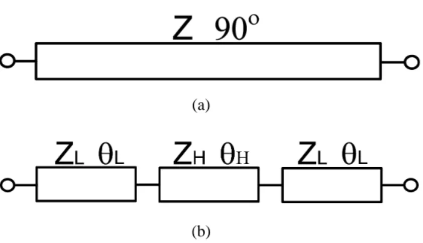
Fig. 2-4. (a) Quarter-wave transmission line (b) Stepped-impedance circuit equivalent to a quarter-wave transmission line
2-1 Analysis of the stepped-impedance line section
The characteristic impedance Z of the hybrid ring corresponding to the specific
return loss can be determined by [17]. A quarter-wave transmission line of impedance Z is shown in Fig. 2-4(a) and it serves as a basic building block of the proposed hybrid ring. Its ABCD matrix is given by
⋅
⎥
⎥
⎦
⎤
⎢
⎢
⎣
⎡
=
⎥
⎦
⎤
⎢
⎣
⎡
0
0
Z
j
jZ
D
C
B
A
(2-1)The quarter-wave transmission line can be replaced by a stepped-impedance structure shown in Fig. 2-4(b) where ZH and ZL are the characteristic impedances of the cascaded sections and θΗ and θL are the corresponding electrical lengths. By choosing ZH>ZL, the overall electrical length of the stepped-impedance section can be
shorter than 900. The ABCD matrix of the stepped-impedance section shown in Fig. 2-4(b) is given by ⎥ ⎥ ⎦ ⎤ ⎢ ⎢ ⎣ ⎡ • ⎥ ⎥ ⎦ ⎤ ⎢ ⎢ ⎣ ⎡ • ⎥ ⎥ ⎦ ⎤ ⎢ ⎢ ⎣ ⎡ = ⎥ ⎦ ⎤ ⎢ ⎣ ⎡ L L L L L L H H H H H H L L L L L L Z j jZ Z j jZ Z j jZ D C B A θ θ θ θ θ θ θ θ θ θ θ θ cos sin sin cos cos sin sin cos cos sin sin cos which gives L H L H L L H L H L H Z Z Z Z Z Z
A [ cos cos2 ( )cos sin sin ]
2
2 θ θ θ
θ
θ − +
H L H H L H L L H L H Z Z Z Z Z j
B [ cos sin ( sin sin cos sin2 )]
2 2 2 θ θ + − θ θ + θ θ = 2 2 2 2 )] 2 sin cos sin sin ( sin cos [ L H L H L L H H H H L L Z Z Z Z Z Z j C= θ θ + − θ θ + θ θ L H L H L L H L H L H Z Z Z Z Z Z
D [ cos cos2 ( )cos sin sin ]
2
2 θ θ θ
θ
θ − +
= (2-2)
Equating the ABCD matrix of the quarter-wave transmission line and the
stepped-impedance structure shown in Fig. 2-4, we have
. 0 sin sin cos ) ( 2 cos cos 2 2 = + − L H L H L L H L H L H Z Z Z Z Z Z θ θ θ θ θ (2-3) . 0 ) 2 sin cos sin sin ( sin cos2 2 2 = − + − + Z Z Z Z Z Z H L H H L H L L H L H θ θ θ θ θ θ (2-4) . 0 1 ) 2 sin cos sin sin ( sin cos 2 2 2 2 = − + − + Z Z Z Z Z Z Z L H L H L L H H H H L L θ θ θ θ θ θ (2-5)
2-2 Design steps of the proposed 1800 hybrid ring coupler
The first step to implement the proposed 1800 hybrid ring coupler is to specify the required return loss. The next step is to replace each line section in Fig. 2-2 by the
stepped-impedance structure. Followings show the procedures. First, arbitrary choose the θΗ and θL and then use (2-3)-(2-5) to find ZH and ZL. Second, check the obtained ZH and ZL to be realizable or not, if not, redo the first step again. Finally, fine-tuning
the obtained circuit parameters might be required to optimize the circuit performance. In this work, the 1800 hybrid ring coupler with 15-dB return loss is designed as an
example and the optimized circuit parameters are shown in Table 2-1.
TABLE2-1
Parameters of the stepped-impedance hybrid ring
ZH
(Ω) (Ω) ZL (Degree)θH
θL (Degree)
Fig. 2-5. Cross-sectional view of the interdigital CPS with N=3.
2-3 Realization and measurement
From [35], we know that the length of a stepped-impedance line can be significantly reduced with larger high- to low-impedance ratios. However, to realize
such high and low impedances simultaneously would be a challenge. Fortunately, this can be solved by using CPS (high impedances) and interdigital CPS (low impedances). The cross-sectional view of the interdigital CPS is shown in Fig. 2-5. Here, N is
defined as the number of CPS strip pair (for instance N=2 has 4 strips) and the conductor thickness (t) is assumed to be zero. The proposed hybrid ring coupler is
fabricated on an Al2O3 alumina substrate with 15-mil thickness (h) and a dielectric constant (εr) of 9.8. It is designed to operate at the center frequency of 2 GHz.
Fig. 2-6 shows the computed characteristic impedance and effective dielectric
constant of CPS as a function of the gap width with the strip width as a parameter. Fig. 2-7 indicates the computed characteristic impedance and effective dielectric constant
of interdigital CPS as a function of the gap width with the number of CPS strip pair as a parameter. It can be found that extremely high impedances can be obtained by conventional CPS with large S and small W and extremely low impedances can be
implemented by interdigital CPS with large N, small S, and large W. Using the design curves in Fig. 2-6 and Fig. 2-7, parameters of each line section corresponding to Table
2-1 can be obtained. In this design, we choose N=3 and the parameters of each line section are listed in Table 2-2. Fig. 2-8 shows the simulated magnitudes of S11 and S21 and the insertion phase difference between two configurations of Fig. 2-3(a) and (b)
with ZH=184Ω, θH=15.20, ZL=22Ω and θL=16.30 where the S-parameters are based on 50-Ω port impedances. Note that all mentioned curves are computed by EM simulator Sonnet. It can be seen that insertion phase difference is within 10 and S-parameters of them are almost the same. Therefore, the proposed configuration in Fig. 2-3(b)
performs perfectly as a wideband phase inverter.
Fig. 2-6. Computed characteristic impedance and effective dielectric constant of CPS as a function of the gap width with the strip width as a parameter, t=0 mil.
TABLE2-2
CPS and Interdigital CPS parameters of the stepped-impedance hybrid ring
Line width W (mil) Gap width S (mil) Z (Ω) Interdigital CPS (N=3) 4 1.6 22 CPS 4 24 184
(a)
(b)
Fig. 2-7. Computed characteristic impedance and effective dielectric constant of interdigital CPS as a function of the gap width with the number of CPS strip pair as a parameter, t=0 mil (a) w=3 mil (b) w=4 mil.
Fig. 2-8. Simulated magnitude of S11 and S21 and insertion phase difference between two
configurations of Fig. 2(a) and (b) with ZH=184Ω, θH=15.20,ZL=22Ω and θL=16.30 where the
S-parameters are based on 50-Ω port impedances.
(b)
Fig. 2-9. Fabricated 1800 hybrid ring coupler (a) Layout (b) Photograph.
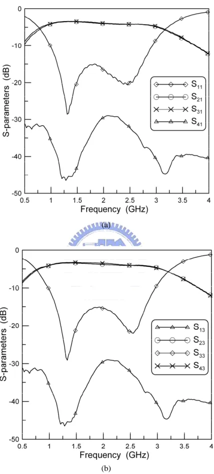
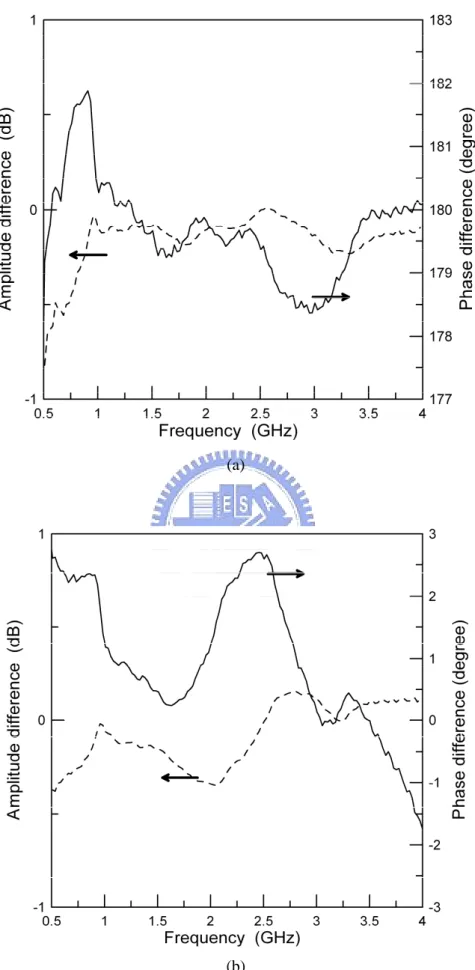
The layout and photograph of the fabricated 1800 hybrid ring coupler are shown in Fig. 2-9. The size of this hybrid is 404 mil × 404 mil. Fig. 2-10 depicts the measured results of the fabricated hybrid ring coupler and the measured insertion loss is
approximately 0.6 dB. The measured return losses are better than 10 dB from 0.98 to 2.93GHz for out-of-phase operation and from 0.97 to 2.96 GHz for in-phase operation,
respectively. The measured isolation is better than 30 dB from 0.5 to 4 GHz. The measured amplitude and phase differences are shown in Fig. 2-11. For out-of-phase operation, the amplitude difference is within 0.5 dB from 0.7 to 4 GHz and the phase
difference is within 20 from 0.5 to 4 GHz. For in-phase operation, the amplitude difference is within 0.5 dB from 0.5 to 4 GHz and the phase difference is within 30
from 0.5 to 4 GHz. Fig. 2-12 shows the measured and simulated results from 0 to 20 GHz. The measured performances of the 1800 hybrid ring coupler are summarized in Table 2-3.
(a)
(b)
Fig. 2-10. Measured results of the fabricated 1800 hybrid ring coupler (a) Out-of-phase operation (b) In-phase operation
(a)
(b)
Fig. 2-11. Measured phase and amplitude differences of the fabricated 1800 hybrid ring coupler (a) Out-of-phase operation (b) In-phase operation.
Fig. 2-12. Measured and simulated results from 0 to 20 GHz.
TABLE 2-3
Summary of measured performances of the 1800 hybrid ring coupler
Out-of-phase In-phase
Frequency range [GHz] (RL< -10dB) 0.98~2.93 (97.5%)
Phase imbalance [Degree] 180 ± 2 0 ± 3
Frequency range [GHz] 0.5 ~ 4
amplitude imbalance [dB] 0 ± 0.4 0 ± 0.5
Frequency range [GHz] 0.75 ~ 4
Chapter 3
Wideband Multi-section 180
0Hybrid Couplers
Using Vertically Installed Planar Couplers
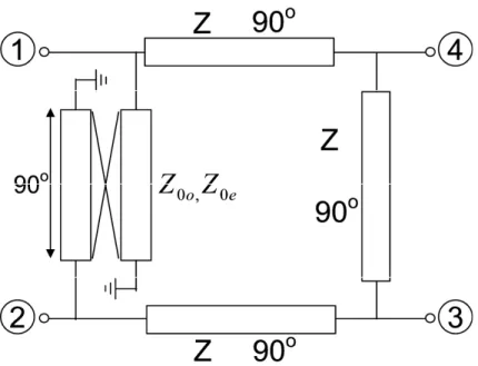
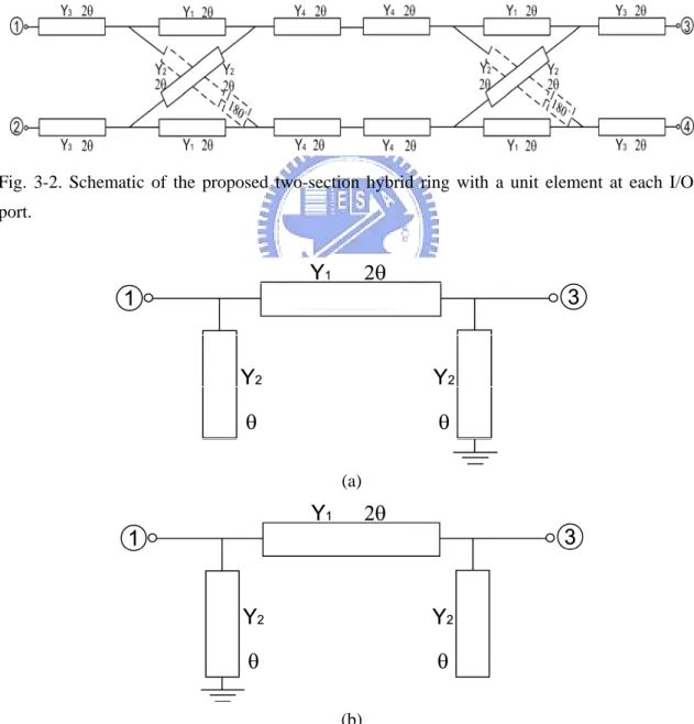
In this chapter, the multi-section 1800 hybrid rings are proposed to overcome the problems of high power-division ratios and broad bandwidth. The basic building block of the proposed multi-section 1800 hybrid ring is the reconfigured ideal 1800
hybrid ring as shown in Fig. 3-1(a) and (b). The proposed single-section hybrid ring can be easily cascaded like the 900 branch-line coupler as depicted in Fig. 3-1(c). The
reconfiguration proposed in Fig. 3-1(b) also results in size reduction. Furthermore, the hybrid ring in Fig. 3-1(b) with two output ports on the same side is convenient for the applications such as balanced-mixer, push-pull amplifier, etc. Synthesis procedures to
realize Chebyshev-response two-section cascaded 1800 hybrid rings shown in Fig. 3-1(c) with various power-division ratios will be described. The reconfigured
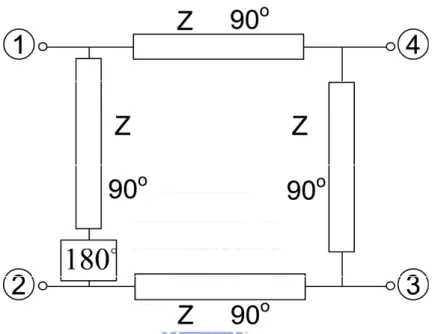
single-section 1800 hybrid ring with a unit element at each port [17], [18] can be cascaded to exhibit extended bandwidth as shown in Fig. 3-2. As an example, the 3-dB two-section hybrid ring with 15-dB return loss yields a bandwidth of 5:1.
However, the realization of a broadband phase inverter on microstrip circuits could be a problem. Fortunately, as described in [6] that a short-ended λ/4 coupled line can provide 2700 phase-shift and the ratio of the even- and odd-mode impedance of the
coupled line determines the bandwidth. The higher even- to odd-mode impedance
ratio produces wider bandwidth. As the ratio approaches to an asymptotic value, the short-ended coupled line is equivalent to a λ/4 line cascaded with an ideal phase inverter. To achieve an enough bandwidth, a very tight coupled line must be
implemented. In this chapter, the VIP coupler described in [36] is proposed to implement the very tight coupled lines. With the VIP coupler, the proposed wideband
multi-section hybrid rings can be easily implemented by microstrip circuits. Several design examples show that the proposed multi-section 1800 hybrid rings not only exhibit broad bandwidth but also depict wide range of power-division ratios.
(a)
(c)
Fig. 3-1. Schematics of hybrid rings using an ideal phase inverter (a) Conventional hybrid ring (b) Reconfigured hybrid ring (c) Proposed two-section hybrid ring.
Fig. 3-2. Schematic of the proposed two-section hybrid ring with a unit element at each I/O port.
(a)
(b)
Fig. 3-3. (a) Even-mode and (b) odd-mode equivalent circuits of the rat-race ring coupler using an ideal phase inverter.
3.1 Theoretical analysis of the two-section hybrid ring
In the reconfigured single-section hybrid ring shown Fig. 3-1(b), the admittance Y1 and Y2 are normalized values with respect to system admittance Y0. Fig. 3-3 shows the even- and odd-mode equivalent circuits of the rat-race ring hybrid using an ideal
phase inverter. Using the even- and odd-mode analysis, the ABCD matrices for the even- and odd-mode cascade elements are given by
⎥ ⎦ ⎤ ⎢ ⎣ ⎡ = ⎥ ⎥ ⎦ ⎤ ⎢ ⎢ ⎣ ⎡ − = ⎥ ⎦ ⎤ ⎢ ⎣ ⎡ D C B A t D t C t t tB t A t D C B A e e e e ) ( ) ( 1 ) ( ) ( ) 1 ( 1 2 1 2 2 2 0 2 1 2 (3-1) ⎥ ⎦ ⎤ ⎢ ⎣ ⎡ = ⎥ ⎦ ⎤ ⎢ ⎣ ⎡ = ⎥ ⎦ ⎤ ⎢ ⎣ ⎡ A C B D A C B D D C B A e e e e o o o o (3-2) where t = jtanθ and the subscripts indicate the degree of the polynomials A(t2
), B(t2), C(t2), and D(t2). The reflection and transmission coefficients of the even- and odd-mode cascade elements are
D C B A C B D A e + + + − + − = Γ ( ) ( ) D C B A C B A D o + + + − + − = Γ ( ) ( ) D C B A T Te o + + + = = 2 (3-3) Therefore, the S-parameters of the single-section hybrid ring can be expressed as
D C B A C B S S s s e o + + + − = Γ + Γ = = ( ) 2 1 22 11 0 ) ( 2 1 21s = Te−To = S D C B A T T S S s s e o + + + = + = = ( ) 2 2 1 42 31 D C B A Y Y D C B A D A S s e o + + + = + + + − = Γ − Γ = ( ) 2( / ) 2 1 2 1 32 D C B A Y Y D C B A A D S s + + + − = + + + − = 2( 2/ 1) 41 (3-4)
The conventional even- and odd- mode analysis method to obtain the S-parameters of the cascaded 900 hybrid ring [20] can not be used in this newly proposed two-section hybrid ring shown in Fig. 3-1(c) because the symmetrical planes for even-
and odd-mode excitation are not exist. Here, the multi-port connection method [37] is
used. The results at the center frequency are shown as follows:
2 4 2 3 2 2 2 1 2 2 2 1 2 4 2 3 44 33 22 11
)
(
)
(
Y
Y
Y
Y
Y
Y
Y
Y
S
S
S
S
+
+
+
+
−
+
=
−
=
−
=
=
0
21=
S
2 4 2 3 2 2 2 1 4 2 3 1 31)
(
2
Y
Y
Y
Y
Y
Y
Y
Y
S
+
+
+
−
−
=
2 4 2 3 2 2 2 1 4 1 3 2 41)
(
2
Y
Y
Y
Y
Y
Y
Y
Y
S
+
+
+
+
=
2 4 2 3 2 2 2 1 4 1 3 2 32 ) ( 2 Y Y Y Y Y Y Y Y S + + + + − = 2 4 2 3 2 2 2 1 4 2 3 1 42 ) ( 2 Y Y Y Y Y Y Y Y S + + + − − = (3-5)When Y1=Y3 and Y2=Y4, all ports can be perfectly matched and the signal incident
at the input port will be split between port 3 and port 4. Although all ports can be
perfectly matched for the case of Y1=Y4 and Y2=Y3, a zero dB coupler, which means
that no signal can be obtained from one of the output ports, is obtained. Therefore, we
concentrate our attention in the case of Y1=Y3 and Y2=Y4. Because in this case the
two-section hybrid ring consists of two identical single-section hybrid rings, the synthesis procedure can be largely simplified. Again, applying the multi-port
connection method to (3-4), we can obtain
) 2 )( 2 )( ( )] 2 ( ) 2 2 ( ) 2 ( [ 2 2 2 2 2 2 2 11 D C A D B A D C B A D CD AC A C D C A B D C A B S + + + + + + + + + + + − + − + + + + = 0 21 = S ) 2 )( 2 ( 4 ) / ( 4 ) 2 )( 2 ( 4 ) ( 2 2 1 2 31 D C A D B A Y Y D C A D B A D A S + + + + − − = + + + + − − − = ) 2 )( 2 ( ) / ( 8 ) 2 )( 2 ( ) ( 4 2 1 41 D C A D B A Y Y D C A D B A D A S + + + + − = + + + + − − =
) 2 )( 2 ( ) / ( 8 ) 2 )( 2 ( ) ( 4 2 1 32 D C A D B A Y Y D C A D B A D A S + + + + = + + + + − = ) 2 )( 2 ( 4 ) / ( 4 ) 2 )( 2 ( 4 ) ( 2 1 2 2 42 D C A D B A Y Y D C A D B A D A S + + + + − − = + + + + − − − = (3-6)
It should be noted that the interchange between Y1 and Y2 results in the interchange
between the sum port and the delta port. Assuming that the input is matched well in the passband, we have
1
2 41 2 31+ S
≈
S
(3-7) The output power-division ratio is2 2 1 2 1 2 2 31 2 41
1
)
/
(
)
/
(
2
⎟⎟
⎠
⎞
⎜⎜
⎝
⎛
−
=
=
Y
Y
Y
Y
S
S
R
(3-8) and (3-7) can be written as1
1
31
+ R
≈
S
(3-9) Now, considering the function
R
S
S
F
+
=
1
31 11 (3-10) where F is approximately equivalent to the reflection coefficient of the two-section hybrid ring over the passband because the denominator is very close to unity [see (3-9)]. Therefore, the insertion loss function PL can be shown as follows:2 2 2 2 2 2 2 2 2 ] 4 ) )[( ( 1 )] 2 ( ) 2 2 ( ) 2 ( [ 2 1 1 − − + + + + + + + + − + − + + + + + = + = D A D C B A R D CD AC A C D C A B D C A B F PL (3-11) As described by Riblet [38], and Carlin and Kohler [39], the insertion loss function of
a Chebyshev response has the form
2 2 2 2 2 2 } 1 2 ) / ( ) 1 1 ( ) / ( ) 1 1 ( { 1 x x x T x x x T x m PL c n c c n c − − − − − + + = − (3-12) where x=cos2θ, xc=cos2θc, Tn(x) is the Chebyshev polynomial of the first kind of
D in (3-1) into (3-11) and fitting (3-11) to (3-12) with n=3, we obtain ) 1 2 ( 1 1 ) 1 )( ( 2 2 1 2 2 1 2 2 2 1 2 1 c c c x x x m R Y Y Y Y Y Y Y = + − + ⎥ ⎥ ⎦ ⎤ ⎢ ⎢ ⎣ ⎡ − ⎟⎟ ⎠ ⎞ ⎜⎜ ⎝ ⎛ − − + (3-13) ) 1 2 2 ( 1 1 ) 2 1 )( ( 3 2 3 2 1 2 2 1 2 2 2 1 2 1 2 1 c c c x x x m R Y Y Y Y Y Y Y Y Y =− + − + ⎥ ⎥ ⎦ ⎤ ⎢ ⎢ ⎣ ⎡ − ⎟⎟ ⎠ ⎞ ⎜⎜ ⎝ ⎛ + + + − + (3-14) The relationship between m and return loss is
dB m
RL=10log(1+1/ 2) (3-15) According to (3-8), (3-13), (3-14), and (3-15), the unknown variables Y1 and Y2 can
be solved numerically. It should be emphasized that there exists two set of solutions.
Let us discuss in the following.
Fig. 3-4. Characteristic impedances Z1, Z2, and bandwidth versus return loss for the
Fig. 3-4 shows the plot of characteristic impedances of Z1, Z2, and bandwidth
versus return loss for the 3-dB two-section hybrid ring shown in Fig. 3-1(c). The 96.3% bandwidth for return loss better than 15dB can be achieved. A similar synthesis procedure can be used to solve the unknown variables for the single-section
hybrid ring. Fig. 3-5 shows the plots of characteristic impedances of Z1, Z2, and
bandwidth versus coupling level, which is defined by the power at coupling port
divided by the incident power, for the single- and two-section hybrid rings with 15-dB return loss. It can be seen that, for the single-section hybrid ring, the bandwidth increases with increasing power-division ratios, but the high impedance value of Z1
limits the realizable power-division ratios to about -10dB. The bandwidth of the two-section hybrid ring decreases with increasing of the power-division ratios but the
values of Z1 and Z2 are both located in the reasonable range for power-division from
as strong as -3dB to weaker than -20dB.
Fig. 3-5. Characteristic impedances Z1, Z2, and bandwidth versus coupling level for the
Fig. 3-6 shows another set of solutions for the two-section hybrid ring. Comparing
to the characteristics of the single-section hybrid ring in Fig. 3-5, it depicts a larger bandwidth, but requires a higher Z1 impedance value. The two-section hybrid ring
shown in Fig. 3-2 comprises two single-section units where each unit has a unit
element at each I/O port. This two-section hybrid ring can achieve larger bandwidth than above described two-section hybrid ring. However, the analysis method
described above is too complicated to obtain similar design equations. Fortunately, values of unknown variables Y1, Y2, Y3, and Y4 can be obtained by optimization with
the known relationship between Y1 and Y2. The design curves for a two-section 3-dB
hybrid of this type are shown in Fig. 3-7.
Fig. 3-6. Another set of characteristic impedances Z1, Z2, and bandwidth versus coupling level
Fig. 3-7. Characteristic impedances Z1, Z2, Z3, Z4, and bandwidth versus return loss for the
equal-ripple response 3-dB two-section hybrid ring with a unit element at each I/O port.
3.2 Characteristics of VIP couplers
Fig. 3-8 shows the cross-sectional view and the parameters of the VIP coupler. Coupling coefficients can be readily controlled by changing the dielectric constants or the thicknesses of the substrates or the height h and width w of the coupler. Therefore,
the newly added vertical substrate can significantly increase the freedom of design. From [36], we know that the electric field is mainly confined in the vertical substrate
for odd-mode excitation and in air and main substrate for even-mode excitation. The equivalent circuit of a short-ended coupled line is shown in Fig. 3-9 where Z0e
and Z0o are the even- and odd-mode characteristic impedances and θ is the electrical
length of the coupled line. When θ=900
, the two shunt shorted stubs of the characteristic impedance Z0e are open-circuited. Therefore, at the center frequency,
the short-ended coupled line is reduced to a λ/4 transmission line of characteristic impedance 2Z0eZ0o/(Z0e-Z0o) cascaded with an ideal phase inverter. It should be
emphasized that previously described theory is based on an ideal single-section 1800 hybrid ring. However, the two shunt shorted stubs in Fig. 3-9 are only open-circuited at the center frequency. Out of center frequency, the influence of this shunt shorted
stub decreases as the value of Z0e increases. Until Z0e approaches to infinity, the
short-ended coupled line is equivalent to the phase inverting arm required in an ideal single-section 1800 hybrid ring. To obtain higher Z0e, we can increase the height h of
the coupler. Comparing Fig. 3-1(b) and Fig. 3-9, it can be found that the value of Z0o
is closed to Z2/2 as long as Z0e is much higher than Z0o. The VIP coupler can not only
realize low values of Z0o but also implement high values of Z0e. Here, the main circuit
is fabricated on a RO4003 substrate with 20-mil thickness (hs) and a dielectric
constant (εr1) of 3.38 and the VIP coupler is implemented on same RO4003 substrate
with 8-mil thickness (hv) and same dielectric constant (εr2) of 3.38. The characteristic
impedances for even- and odd-modes of the VIP couplers can be obtained by the fully
Fig. 3-9. Equivalent circuit of a short-ended coupled line.
TABLE3-1
VIP coupler parameters extracted by HFSS (f0=2 GHz)
Z (Ω) H (mil) W (mil) εre εro Z0e (Ω) Z0o (Ω) L (mil) 59.0 70 21.5 1.28 2.87 348.0 27.2 894.0 50.8 70 25.9 1.26 2.91 336.0 23.5 886.0 41.3 70 34.0 1.24 2.97 320.6 19.4 875.5 29.8 70 49.0 1.22 3.04 297.5 14.2 862.0
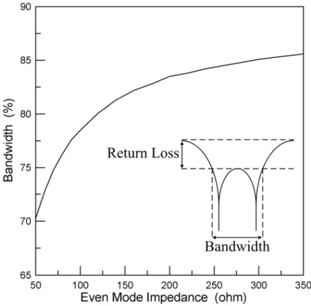
Four cases of VIP couplers are calculated for the prototype circuits in the next section. The physical parameters in Fig. 3-8 and the calculated electrical parameters
of the VIP couplers are listed in Table 3-1 where L is the required physical length of the short-ended VIP coupler to provide 2700 phase-shifting at the center frequency of 2GHz. Fig. 3-10 shows the simulated 15-dB equal-ripple return loss bandwidth of a 3-dB single-section hybrid ring with a short-ended coupler versus different Z0e. It can
be seen that the bandwidth approaches to an asymptotic value as long as Z0e is higher
than about 250Ω. Therefore, if the VIP coupler can have this high Z0e value, a nearly
ideal single-section unit can be implemented. Besides, the VIP coupler can also
provide a good crossover in the proposed circuit. Because the signal going through the short-ended VIP coupler is mainly odd-mode and the field of odd-mode is mostly confined in the VIP substrate, the crossover has negligible influence on circuit
Fig. 3-10. Simulated 15-dB equal-ripple return loss bandwidth of a 3-dB single-section hybrid ring with a short-ended coupler versus different Z0e.
3.3 Experimental results and discussion
As we mentioned previously, the VIP coupler is a good candidate to realize the phase inverter and the crossover on microstrip circuits. Four prototype circuits are
fabricated that all of them are with a 15-dB of equal-ripple return loss. Four prototype circuits are a single-section reconfigured 3-dB hybrid ring to observe the performance of the single-section building block, a two-section 3-dB hybrid ring with the
equivalent circuit shown in Fig. 3-1(c) to verify the validity of the theory derived in previous section, a two-section 20-dB hybrid ring to show the high power-division
ratio of the proposed design in Fig. 3-1(c), and a two-section 3-dB hybrid ring with the equivalent circuit shown in Fig. 3-2 to depict the bandwidth extension performance.
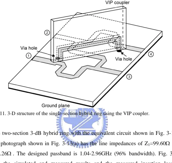
The 3-D view of the reconfigured single-section hybrid ring is shown in Fig. 3-11 and the photograph of the reconfigured and conventional 3-dB hybrid rings is depicted in Fig. 3-12. The required VIP coupler parameters with Z=59Ω are also shown in Table 3-1. It can be seen that the reconfigured single-section hybrid ring is
compact compared to the conventional one. The measured performance, although not
shown, is very close to theoretical results. This is the basic building block of next three two-section hybrids.
Fig. 3-11. 3-D structure of the single-section hybrid ring using the VIP coupler.
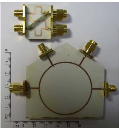
The two-section 3-dB hybrid ring with the equivalent circuit shown in Fig. 3-1(c)
and a photograph shown in Fig. 3-13(a) has the line impedances of Z1=99.60Ω and
Z2=41.26Ω . The designed passband is 1.04-2.96GHz (96% bandwidth). Fig. 3-14
shows the simulated and measured results and the measured insertion loss is approximately 0.4dB. The measured return losses are better than 10 dB from 1.06 to
3GHz for out-of-phase operation and from 1.16 to 3.04GHz for in-phase operation, respectively. The measured isolation is typically better than 20 dB from 0.5 to 3.5 GHz. The measured amplitude and phase imbalances are shown in Fig. 3-15. For
out-of-phase operation, the amplitude imbalance is within 1 dB from 1.06 to 3.1GHz and the phase imbalance is within 100 from 1.08 to 3.5GHz. For in-phase operation, the amplitude imbalance is within 1 dB from 0.96 to 3.5GHz and the phase imbalance
is within 100 from 0.5 to 3.5GHz. The required VIP coupler parameters with Z=41.3Ω are shown in Table 3-1.
Fig. 3-12. Fabricated circuits of the conventional and reconfigured single-section hybrid rings.
The two-section 20-dB hybrid ring with the equivalent circuit shown in Fig. 3-1(c)
and a photograph shown in Fig. 3-13(b) has line impedances of Z1=56.21Ω and
Z2=50.84Ω. The measured and simulated results are shown in Fig. 3-16. The designed
passband is 1.144-2.856GHz (85.5% bandwidth). The measured equal-ripple return loss bandwidth is a little narrower than the simulated result. The measured isolation is better than 25 dB from 0.5 to 3.5 GHz. The measured phase performances are not
shown here because they are not important for loose coupling. The required VIP coupler parameters with Z=50.8Ω are shown in Table 3-1. In contrast, a single section 20-dB hybrid ring with unit element should have Z1=364.1Ω, Z2=36.41Ω, and ZT
(impedance of a unit element) =38.9Ω which can hardly be realized by microstrip or CPW circuit. The single section 20-dB hybrid ring without unit element has higher
impedance values that are more difficult to implement.
The two-section 3-dB hybrid ring with the equivalent circuit shown in Fig. 3-2 and
a photograph shown in Fig. 3-13(c) has the line impedances of Z1=71.48Ω,
Z2=29.61Ω, Z3=34.29Ω, and Z4=29.12Ω. The designed passband is 0.66-3.34GHz
measured insertion loss is approximately 0.6dB. The measured return losses are better
than 10 dB from 0.72 to 3.38GHz for out-of-phase operation and from 0.82 to 3.36GHz for in-phase operation, respectively. The measured isolation is better than 20 dB from 1.16 to 3.5 GHz. The measured amplitude and phase imbalances are shown
in Fig. 3-18. For out-of-phase operation, the amplitude imbalance is within 1 dB from 0.72 to 3.5GHz and the phase imbalance is within 100 from 0.9 to 3.3GHz. For in-phase operation, the amplitude imbalance is within 1 dB from 0.72 to 3.36GHz and the phase imbalance is within 100 from 0.76 to 3.38GHz. The required VIP coupler parameters with Z=29.8Ω are shown in Table 3-1.
(a) (b)
(c)
Fig. 3-13. Fabricated two-section hybrid rings (a) 3-dB hybrid ring (b) 20-dB hybrid ring (c) 3-dB hybrid ring with a unit element at each I/O port.
(a)
(b)
Fig. 3-14. Measured and simulated results of the 3-dB two-section hybrid ring (a) Out-of-phase operation (b) In-phase operation.
(a)
(b)
Fig. 3-15. Measured amplitude and phase imbalances of the 3-dB two-section hybrid ring (a) Out-of-phase operation (b) In-phase operation.
Fig. 3-16. Measured and simulated results of the 20-dB two-section hybrid ring.
(b)
Fig. 3-17. Measured and simulated results of the 3-dB two-section hybrid ring with a unit element at each I/O port (a) Out-of-phase operation (b) In-phase operation.
(b)
Fig. 3-18. Measured amplitude and phase imbalances of the 3-dB two-section hybrid ring with a unit element at each I/O port (a) Out-of-phase operation (b) In-phase operation.
The above measured results indicate the bandwidth of the two-section cascadable hybrid rings using the VIP coupler is a little narrower than that using an ideal phase inverter, especially for in-phase operation. It should be point out that the simulated
performances in Figs. 3-14, 3-16, and 3-17 are based on an ideal single-section unit. The bandwidth shrinkage is due to the fact that the infinity value of Z0e is impractical
to be fabricated. In previous section, we have shown that if the Z0e higher than 250 Ω,
the performance of a single-section unit approaches to an ideal hybrid ring. Nevertheless, the characteristics of a single-section unit equal to those of an ideal
hybrid ring only when Z0e is infinity. Therefore, the bandwidth is shrunk due to finite
Z0e especially in the cascaded case. In addition, the junction effect (especially
junctions at microstrip and VIP coupler) and circuit fabricating imperfections degrade the bandwidth further.
Chapter 4
Wideband Bandpass Filters with Wide Upper
Stopband Using Stepped-Impedance Rat-Race
Hybrid Couplers
In this chapter, we propose the wideband bandpass filter using two 1800 hybrid ring couplers. Then, by adding one pair of quarter-wave transmission lines between two hybrid ring couplers, this filter can exhibit wider bandwidth. Finally, by employing
two pairs of quarter-wave transmission lines, the two rat-race hybrid couplers can be connected without crossover. In addition, compared to the basic structure, using two
pairs of quarter-wave transmission lines for connections can increase the order and bandwidth of the filter. Therefore, we use two rat-race hybrid couplers and two pairs of quarter-wave transmission lines with a stepped-impedance structure to design a
wideband bandpass filter. The filter with the stepped-impedance structure acquires not only size reduction, but also better upper stopband clearance.
Fig. 4-1. Schematic of the proposed wideband bandpass filter using two 1800 hybrid ring couplers.
4.1 Bandpass filter by cascading two 1800 hybrid couplers
Fig. 4-1 shows the schematic of the proposed wideband bandpass filter using two 1800 hybrid ring coupler. It should be noted that the schematic shown in Fig. 4-1 is
different from that shown in Fig. 3-1(c) at the connections of ports. Based on the analysis method mentioned in section 3.1, the S-parameters of the proposed wideband bandpass filter shown in Fig. 4-1 can be expressed as
) 2 )( 2 )( ( ) 2 ( 2 )] 2 2 ( ) 2 ( [ 2 2 2 2 2 2 2 44 33 22 11 D C A D B A D C B A D CD AC A C D C A B D C A B S S S S + + + + + + + + + + + − + − + + + + = = = =
0
43 21= S
=
S
0
42 31= S
=
S
. ) 2 )( 2 ( ) ( 4 2 32 41 D C A D B A D A S S + + + + − + = = (4-1) All of the power excited at port 1 will be delivered to port 4 and no power reaches port 3 and port 2. Also, we can obtain. 0 ) 1 2 ( ) 1 )( ( 2 2 2 2 1 2 2 2 1 2 1 − + − = + − − + c c c x x x m Y Y Y Y Y Y (4-2) . 0 ) 1 2 2 ( ) 2 1 )( ( 3 2 3 2 2 2 1 2 2 2 1 2 1 2 1 + + − = + + + + − + c c c x x x m Y Y Y Y Y Y Y Y (4-3)
The relationship between m and return loss (RL) is . ) / 1 1 log( 10 m2 dB RL= + (4-4) Here, we assume that the relationship between Y1 and Y2 is
.
2 1
r
Y
Y =
(4-5)Equations (4-2)-(4-5) can be used to design the wideband bandpass filter with a given
return loss and relationship r between Y1 and Y2. Fig. 4-2 and Fig. 4-3 show the plots of Z1 and Z2 versus bandwidth for 15-dB and 20-dB equal-ripple return loss,
respectively. It can be found that the higher Z2 to Z1 impedance ratio is, the broader the bandwidth of the filter can achieve.
Fig. 4-2. Characteristic impedances Z1 and Z2 versus bandwidth for the wideband bandpass
Fig. 4-3. Characteristic impedances Z1 and Z2 versus bandwidth for the wideband bandpass
filter with 20-dB equal-ripple return loss.
The wideband phase inverter formed by a FGCPW (finite ground-plane-width
CPW) twisted line can be adopted for the realization of this proposed filter. In the mean time, there are two crossovers as shown in Fig. 4-1. Fortunately, phase inverters and crossovers can be combined. The circuit configuration of the realized phase
inverter and crossover using FGCPW is shown in Fig. 4-4. This wideband bandpass filter is fabricated on an Al2O3 alumina substrate with 15-mil thickness and a
dielectric constant of 9.8. The wideband bandpass filter with 15-dB return loss has the
line impedance of Z1=Z2=53.31Ω which corresponds to a passband of 1.15-2.85GHz (85% bandwidth). Fig. 4-5 shows the photograph of the proposed filter where port 1 and port 4 are terminated with 50-Ω resistors. Here, the port 2 is input port and port 3 is output port as depicted in Fig 4-1. It should be note that port 1 and port 4 can also
be open-circuit or short-circuit because of good isolations in port 1 and port 4. Fig. 4-6 shows the simulated and measured results. The measured passband insertion loss is approximately 1.2dB. The measured results match very well with the simulated
results.
Fig. 4-6. Measured and simulated results of the wideband bandpass filter.
4.2 Bandpass filter by cascading two stepped-impedance 1800 hybrid couplers with one unit element
(a)
(b)
Fig. 4-7. Schematics of the proposed wideband filters (a) Basic structure (b) Modified structure .
Although the bandpass filter shown in Fig. 4-1 exhibits wide bandwidth, it still has
the spurious problem. Now, consider the two-section hybrid ring shown in Fig. 4-7(a) and its S-parameters at the center frequency are
0
22 11= S
=
S
0
43 21= S
=
S
2 2 2 1 2 2 2 1 42 31S
(
Y
Y
)
/
Y
Y
S
=
=
−
−
+
) /( 2 22 2 1 2 1 32 41 S YY Y Y S =− = + . (4-6) When Y1=Y2, the signal excited at port 1 is equally divided between 3’ and 4’ and nopower reaches 2’. The signal arriving at 3’ and 4’ are out of phase. Then, the signal at 3’ is equallydivided between 3” and 4” and the signal arriving at 3” and 4” are out of
phase. The signal at 4’ is equally divided between 3” and 4” and the signal arriving at 3” and 4” are in phase. Therefore, all of the power excited at port 1 will be delivered to port 4 and no power reaches port 3 and port 2 (corresponding to a 0-dB coupler).
This means that a bandpass response can be obtained by cascading two 3-dB 180o hybrid rings.
Fig. 4-8. Characteristic impedances Z1, Z3, and bandwidth versus return loss for the
Fig. 4-9. Simulated results of the proposed wideband filter (a) Basic structure (b) Modified structure.
Here, to increase the order and the bandwidth of the proposed filter, a 900 transmission line of impedance Z3 can be added between two 180o hybrids as shown
in Fig.4-7(b). With the design method described in section 3.1, the bandwidth of this filter corresponding to specific return losses can be obtained. Fig. 4-8 shows the plot
of characteristic impedances of Z1, Z3, and bandwidth versus return loss for the
bandpass filter shown in Fig. 4-7(b).
The simulated results of the filters in Fig. 4-7(a) and 4-7(b) with 15-dB return loss
are depicted in Fig. 4-9 that they correspond to third (Z1=Z2=53.31Ω) and fourth
(Z1=Z2=58.65Ω and Z3=41.16Ω) order filter respectively. Although wide passband
can be easily achieved, the first spurious passband at 3f0 results in poor upper
stopband performance. In chapter 2, the frequency of the first spurious response of the 180o hybrid ring can be moved using the stepped-impedance structure by adjusting its structural parameters. Thus, by applying the stepped-impedance structure to Fig. 4-7(b), a wideband filter with broad upper stopband characteristics can be obtained.
The design procedures are summarized as follow:
Step 1) Specify the required return loss and obtain the corresponding circuit parameters in Fig. 4-7(b). This can be easily obtained from Fig. 4-8. (15dB-