Central European Journal of
Chemistry
Electrical and Optical Properties of a Single
Sb
2
Se
3
Nanorod
* E-mail: [email protected]
Received 25 June 2008; Accepted 11 September 2008
Abstract: In this paper we present the methods to chemically synthesize the Sb2Se3 nanorods and study the electrical and optical properties of a
single Sb2Se3 nanorod with an average size of 70 nm in diameter and a length of about 1 mm to 2 mm. The techniques we devised can
immobilize and allocate a single nano-object on an electron beam (E-beam) patterned smart substrate. It can also overcome the limita-tion of the spatial resolulimita-tion of convenlimita-tional optical techniques (~ 1 mm) to obtain optical spectroscopy in an individual nano-object less than 100 nm in size. We also demonstrate the techniques in using E-beam defined metallic coordination markers as electrodes to measure the conductance of a single Sb2Se3 nanorod.
© Versita Warsaw and Springer-Verlag Berlin Heidelberg.
Keywords:Nanorod • Conductance • Photoluminescence • Electron beam lithography 1 Department of Applied Chemistry and Institute of Molecular Science,
National Chiao Tung University, 30010 Hsinchu, Taiwan
2 Department of Chemistry, National Dong Hwa University,
Hualien 97401, Taiwan
T.Y. Ko
1, C.H. Yang
1, K. W. Sun
1*, H.W. Chang
2, B. Sarkar
2, C.W. Liu
2SSC-2008
1. Introduction
In recent years, antimony triselenide (Sb2Se3), which
is a layer-structured semiconductor of an orthorhombic crystal structure, has attracted considerable attention due to its switching effects [1] and good photovoltaic and thermoelectric properties [2,3]. Thin polycrystalline films of Sb2Se3 semiconductors are commonly used as
absorber films for the fabrication of cost-effective solar cells and Hall effect devices [4]. Its high thermoelectric power allows possible applications for optical, thermoelectric cooling, and power conversion devices [5].
Over the last decade, various methods have been demonstrated on the synthesis and characterization of one-dimensional (1D) nanostructure V-VI group semiconductor compounds. These 1D nanostructures can be used as building blocks for many novel functional materials and devices. The synthesis of Sb2Se3 nanorods
has been demonstrated using a hydrothermal reduction route [6]. It was found that hydrazine as both the reducing agent and the coordinator was crucial for the
formation of the rod-like morphologies. The solvothermal synthesis of crystalline Sb2Se3 nanowires with a high
aspect ratio in diethylene glycol media was reported by Wang et al. [7]. Nanoribbons with diameters in the range of 25 to 100 nm and length of 10s of micrometers have been synthesized via a simple hydrothermal process [8]. More recently, Zhang et al. [9] reported the synthesis of Sb2Se3 hollow nanospheres prepared by
solvothermal treatment of SbCl3 and selenium powder
in the presence of cetyltrimethyl ammonium bromide (CTAB). The control synthesis of novel Sb2Se3 and
Sb2S3 nanostructures with a sheaf-like and dumbbell
morphology was demonstrated under hydrothermal treatment in the presence of poly-(vinyl pyrrolidone) PVP polymer by Chen and co-workers [10].
In this work, we demonstrate the synthesis of nanocrystalline Sb2Se3 from the single source precursor
Sb[Se2P(OiPr)2]3 at different temperatures. The
optical and transport properties of the single Sb2Se3
nanostructure were measured at room temperature by dispersion, immobilization, and allocation of a single nanorod on silicon substrates patterned with coordination markers using E-beam lithography techniques.
Electrical and Optical Properties of a Single Sb2Se3 Nanorod
2. Experimental Procedures
2.1. Synthesis of Sb
2Se
3nanorods
The synthesis of the Sb[Se2P(OiPr)2]3 precursor followed
the modified procedure reported by Zingaro et al. [11] that had been used to prepare the Sb[Se2P(OEt)2]3. A
suspension of NH4[Se2P(OiPr)2]3 (1.00 g, 3.067 mmol)
in 40 mL of dichloromethane was added to Sb(OAc)3 (0.306 g, 1.025 mmol), and the resulting mixture was stirred for 4 h under N2. The reaction mixture was filtered
through Celite under a N2 atmosphere; the yellow filtrate
was collected and evaporated to dryness using a rotary evaporator under reduced pressure. The resulting solid was dissolved in hexane (20 mL), filtered through Celite, and evaporated to dryness. After evaporation of the solvent, the yellow powder Sb[Se2P(OiPr)2]3
was collected. A single crystal suitable for X-ray crystallography was grown from dichloromethane layered with hexane.
The nanorods were prepared by a solvothermal method from the single-source precursor Sb[Se2P(OiPr)2]3. Sb[Se2P(OiPr)2]3 (0.8 g, 0.767 mmol)
was added to 20 mL of methanol and heated in a Teflon-coated stainless steel autoclave at either 100 oC or 150oC
for 12 h. After cooling to room temperature, the product appeared as a black solid. The solid was washed with methanol (1 mL × 3 times) and dried at 70oC for 5 h.
The composition of the solid was found by powder X-ray diffraction (XRD) and energy dispersive spectrometer (EDS) to be Sb2Se3. More details on the preparation of
the precursor and the synthesis of Sb2Se3 nanorods can
be found in [12,13].
2.2. Spectroscopy of a single nanorod
We first diluted the 0.001 g of Sb2Se3 nanorod powder
fabricated at 100oC in 10 ml deionized (DI) water and
ethanol mixture. The solution was then placed in an ultrasonic bath operated at a vibration frequency of 185 KHz for 30 min to prevent the formation of nanorod clusters. Due to the acoustic cavitation effect [14], the ultrasonic wave heated up the water and broke the water molecules into H+ and OH- ions. The OH- ions
attached to the nanorod surface and induced a Coulomb repulsion force between the nanostructures. Therefore, the clustering of the nanorods was avoided. A test drop of the solution was placed on a bare Si wafer, and after the solution had dried out, the scanning electron microscope (SEM) images were taken to examine the clustering of the nanorods. The concentration of the solution was continuously adjusted until the nanoparticles were well dispersed on the template. The preparation of the patterned smart substrates is explained as follows.
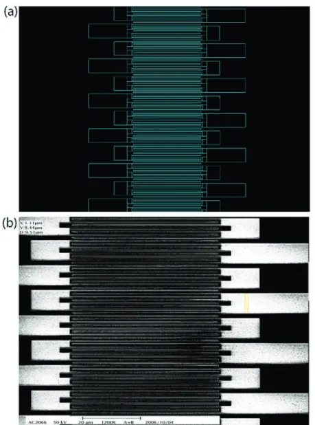
We designed and fabricated a coordination system on Si templates for labeling a dispersed single nanorod. The templates used in the experiments were commercially available 4-inch silicon wafers with (001) crystal orientation and n-type background doping. The Si wafer was first diced into 2 cm × 2 cm chips. As shown in Fig. 1(a), a pattern of two-dimensional array cross-finger type metal wires with a linewidth of 500 nm, a pitch of 1 mm, and a length of 50 mm was defined on the Si chip using E-beam lithography within an area of 1 mm2. On
the right- and left-hand sides of the patterned area, we defined a series of rectangular and square position markers (with dimensions of 10 mm × 30 mm and 10 mm × 10 mm, respectively), so the coordinates could be easily counted under an optical microscope. The pitch and metal linewidth were determined according to the laser spot size ( ~ 1 mm ) and optical resolution of our confocal microscope ( ~ 300 nm ) at the excitation wavelength of 532 nm. The SEM image of the E-beam defined pattern is shown in Fig. 1(b). A drop of the well diluted Sb2Se3 nanorod solution was placed on the
patterned template.
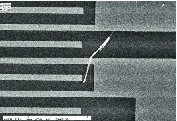
After the sample had dried out, the surface was scanned by SEM to allocate a single nanorod. Fig. 2
shows the SEM scanning results of a single nanorod with a diameter of 70 nm and a length of 2 mm. Most importantly, from the SEM image, we were able to ensure that there was no other nanorod within the laser focus spot but the selected target before the optical measurements. After the target was allocated, their corresponding coordinates were assigned. Fig. 3
shows the optical image of the patterned substrate. The dimension of the coordination markers was properly designed so they could still be clearly seen under the optical microscope. The entire template was moved via an X-Y stepping motor to the given coordinate to position the targets under the laser spot, while the optical image of the substrate was simultaneously monitored on a TV screen. The optical signals were collected at room temperature through the microscope objective and were analyzed by a 0.32 m spectrometer equipped with a liquid nitrogen cooled CCD detector at the excitation wavelength of 532 nm. The optical signal was further optimized by adjusting the focal plane position along the z-axis via the piezo-driven objective lens. The acquired spectra were averaged to achieve a good signal-to-noise ratio.
2.3. Conductivity measurement of a single
nanorod
The E-beam defined cross-finger type position markers can also serve as the electrodes for the transport measurements on a single object basis. After a
single nanorod was selected, a focus ion beam (FIB) was used to selectively deposit Platinum (Pt) metal contacts on both ends of the rod. A thin Pt metal wire was also sputtered using the FIB to make connections between the metal contacts and the nearby electrodes (coordination markers). The surface of the Si substrate was first passivated with a thermally-grown SiO2 layer
with a thickness of 1000 Å before the fabrication of the metal coordination markers to avoid leakage of current through the substrate during the current–voltage (I-V) measurement. The I-V characteristics of a single nanorod were probed at room temperature with an HP-4145 probe station under a current sensitivity of 1 pA.
3. Results and Discussion
The SEM images of the fabricated nanorods at 100oC
and 150oC are shown in Fig. 4 (a) and (b), respectively.
The Sb2Se3 nanorods made at 100oC have an average
diameter of 30 nm to 50 nm and an average length of 2 mm to 3 mm. However, for the rods made at 150oC,
the SEM images show a slightly larger diameter of 70 nm to 90 nm and an average length of 3 mm to 5 mm. Fig. 5 shows the XRD pattern of the nanorods. Synthesis at both temperatures can be indexed with the orthorhombic crystal system with the space group Pnma, and the cell parameters a = 11.63 Å, b = 3.99 Å, and c = 11.78 Å were able to meet the standard values in the Joint Committee on Powder Diffraction Standards
Figure 1. (a) Schematics of the cross-finger type coordination markers and (b) SEM image of the E-beam defined pattern after photolithography processes.
Electrical and Optical Properties of a Single Sb2Se3 Nanorod
Figure 3. The optical image of the patterned substrate through the microscope.
(JCPDS) 15-0861 documents. In short, the intrinsically anisotropic, layered crystalline structure of Sb2Se3 plays
an important role in favoring the crystal growth along the formation of 1D nanostructures. If we think of the Sb2Se3 structure as made up of puckered sheets or
planes of stoichiometric composition running parallel to the c-axis, and close to the [010] directions. The binding between these sheets is much weaker than that within the sheets. Considering the strong Sb-Se bonds, these sheets consist of infinite chains of Sb2Se3 parallel to the
c-axis. Consequently, Sb2Se3 breaks easily along the
c-axis, thus leading to the formation of 1D structure.
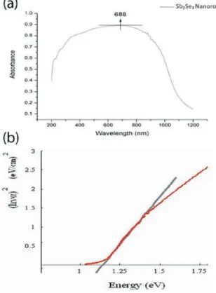
The UV-visible light absorption spectrum of the nanorod clusters in the range of 200 nm to 1200 nm, as shown in Fig. 6 (a), has a maximum of 688 nm. The absorption coefficient a is determined by the following
Figure 4. The SEM images of the fabricated Sb2Se3 nanorods at (a) 100oC, the nanorods have an average diameter of 30 ~ 50 nm and a length
of 2 ~ 3 mm and (b) 150oC, the nanorods have an average diameter of 70 ~ 80 nm and a length of 3 ~ 5 mm.
Figure 5. The XRD pattern of the Sb2Se3 nanorods (Sb2Se3
stan-dard: Joint Committee on Powder Diffraction Standards (JCPDS) 15-0861).
Figure 6. (a) The UV-visible light absorption spectrum and (b) the calculated absorption coefficient as a function of energy
Electrical and Optical Properties of a Single Sb2Se3 Nanorod equation: E E E B n g)] ( [ � = � ,
where E=� , B is determined by the effective mass of the valence band and conduction band and n = ½ for the direct band material. Fig. 6 (b) shows the absorption coefficient as a function of energy. The extrapolation of this curve gives the energy of the direct band gap (Eg) at
1.17 eV. The estimated band gap energy of our nanorods is comparable to the value (1.13 eV) reported in [10], which is also not affected by the quantum confinement effect.
Photoluminescence of more than 200 nm in full width at half maximum (FWHM) and centered at 710 nm was observed from the nanorod powder. However, for
Figure 7. Photoluminescence spectrum of a single Sb2Se3 nanorod.
the single nanorod, a narrower PL emission centered at about 700 nm with an FWHM of 125 nm was observed at an excitation wavelength of 532 nm as shown in Fig. 7. The broader linewidth of the nanorod powder is due to the size distribution of the rods. The exponentially decaying tail near 560 nm in Fig. 7 is due to the Si Raman signal from the substrate. The features on this broad emission can be fitted with a single Lorentzian peak centered at 695 nm, although similar PL results were reported by Ma et al. [15] on wire-like microcrystalline Sb2Se3 powder excited with UV laser light. Their experimental results indicated a PL peak at 707 nm but with a much narrower FWHM of only 25 nm. The broad emission peaks observed in our experiment originate from the increasing number of surface defects, impurities, and dangle bonds attached to the surface as the dimensions of the nanostructures were reduced from micrometer to nanometer scale.
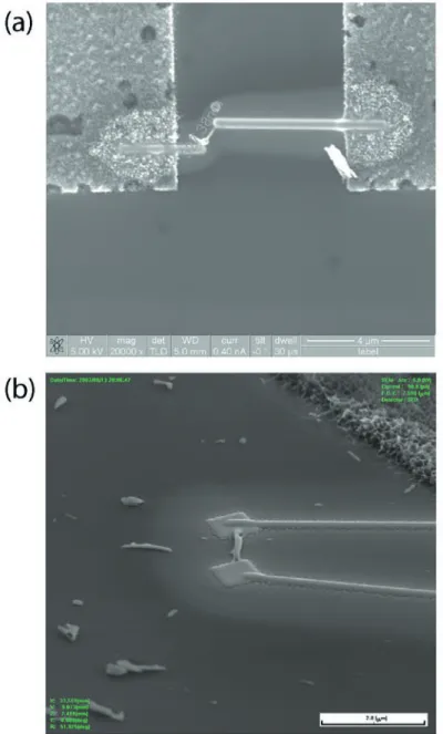
Fig. 8 shows the SEM image of the two-point electrical contact made on a single Sb2Se3 nanorod with
a diameter of 70 nm and a length of about 0.5 mm. The Pt metal wires sputtered with FIB were used to connect both ends of the rod to the nearby electrodes. The total resistance between the two probes can be expressed by the following equation:
2 3 2 2 2 T p c sp s Sb Se V R R R R R R I = = + + + + ,
where Rsp represtents the spreading resistance, Rp is
the probe resistance, and Rs and Rc are the sheet ad
contact resistance, respectively. By directly shortening the probes and the contact pads, the values of Rp and Rsp + Rs can be determined. The measured values of Rp and 2Rsp + 2Rs are 1.87�and 55�, respectively,
which is negligible compared to the Rc and RSb2Se3.
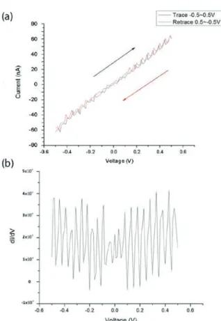
The sample was annealed after the deposition of Pt to reduce the contact resistance. Fig. 9 (a) shows the I-V characteristics of a single nanorod. The slope of the curve gives a resistance of about 10 M�, which is the value of typical semiconductors.
The I-V curve also shows an interesting oscillatory behavior between the applied voltage of -0.4 V and 0.6 V. The first-order differentiation of the curve, as shown in Fig. 9 (b), shows a clear oscillation period of 0.04 V. This phenomenon is attributed to the chain-like structures of the Sb2Se3 nanorod [7], which leads to the trapping of
multiple electrons. The number of trapped electrons changes successively from 0 to 1, to 2 and so forth when the external source is increased. At zero temperature, the current can only flow during the charge configuration transition and lead to an additional Coulomb staircase in the I-V curve [16]. However, thermal fluctuation can give the trapped electrons a finite probability to tunnel to a nearby vacancy or defect site. When such tunneling takes place, trapped electrons escape from the current charge configuration and the configuration is destroyed. The charge configuration can be restored later when the voltage source supplies the necessary number of electrons. The sequence of break-up and restoration of the charge configuration repeats. Therefore, a current can flow in the Coulomb blockade gaps.
4. Conclusion
In summary, we demonstrated a solvothermal method for synthesizing the nanocrystalline Sb2Se3 rods from
a single source precursor. By combining a confocal microscope and an E-beam patterned smart substrate, we were able to study the photoluminescence and electrical properties of the nanorods on a single nanostructure basis. In contrast to earlier reports on Sb2Se3 nanostructure powder or clusters, the factors
arising from size distribution can be ruled out. The observed broad linewidth of the luminescence spectra from the single rod can be attributed to the increased number of surface defects, impurities and dangle bonds attached to the surface as the nanoparticle size is reduced to nanometer scale. The oscillatory behavior
Figure 9. (a) The I-V characteristics of the single nanorod and (b) The first order differentiation of the I-V curve shown in (a).
Electrical and Optical Properties of a Single Sb2Se3 Nanorod
observed in the I-V curve is attributed to a new type of Coulomb blockade gap and fluctuation-induced Coulomb staircase.
Acknowledgement
This work was supported by the National Science Council of the Republic of China under contract No. NSC 96-2112-M-009- 024 –MY3 and the MOE ATU program.
References
[1] N.S. Platakis, H.C. Gatos, Phys. Status Solidi A13 K1 (1972)
[2] J. Black, E.M. Conwell, L. Sigle, C.W. Spencer, J. Phys. Chem. Solids 2, 240 (1957)
[3] K.Y. Rajapure, C.D. Lokhande, C.H. Bhosele, Thin Solid Films 311, 114 (1997)
[4] V.B. Nascimento, V.E. de Carvalho, R. Paniago, E.A. Soares, L.O. Ladeira, H.D. Pfannes, J. Electron Spectrosc. 104, 99 (1999)
[5] K.Y. Rajpure, C.D. Lokhande, C.H. Bhosale, Mater. Res. Bull. 34, 1079 (1999)
[6] J. Wang, Z. Deng, Y. Li, Mater. Res. Bull. 37, 495 (2002)
[7] D. Wang, D. Yu, M. Shao, W. Yu, Y. Qian, Chem. Lett. 31, 1056 (2002); J. Crystal Growth 253, 445 (2003)
[8] Q. Xie, Z. Liu, M. Shao, L. Kong, W. Yu, Y. Qian, J. Crystal Growth 252, 570 (2003)
[9] Y. Zhang, G. Li, B. Zhang, L. Zhang, Mater. Lett. 58, 2279 (2004)
[10] G.-Y Chen, B. Dneg, G.-B. Cai, T.-K. Zhang, W.-F. Dong, W.-X. Zhang, A.-W. Xu, J. Phys. Chem. C 112, 672 (2008)
[11] V. Krishnan, R.A. Zingaro, Inorg. Chem. 8, 2337 (1969)
[12] Y.-F. Lin, H.-W. Chang, S.-Y. Lu, C.W. Liu, J. Phys. Chem. C 111, 18538 (2007)
[13] H.-W. Chang, B. Sarkar, C.W. Liu, Crystal Growth & Design 7, 2691 (2007)
[14] H. Richer, Z.P. Wang, L. Ley, Solid State Commun. 39, 625 (1981)
[15] X. Ma, Z. Zhang, X. Wang, S. Wang, F. Xu, Y. Qian, Journal of Crystal Growth 263, 491 (2004)
[16] M. Shin, S. Lee, K.W. Park, E.-H. Lee, Supperlattices and Microstructures 25, 279 (1999)