The Strong Degradation of 30 Å Gate Oxide Integrity
Contaminated by Copper
Y. H. Lin,aY. C. Chen,bK. T. Chan,aF. M. Pan,cI. J. Hsieh,band Albert China,,z a
Department of Electronics Engineering, National Chiao Tung University, Hsinchu, Taiwan bDepartment of Electric Engineering, Chung Hua University, Hsinchu, Taiwan
c
National Nano-Device Laboratory, Hsinchu, Taiwan
A much higher leakage current, a lower breakdown effective field, a poorer charge-to-breakdown, and worse stress-induced leakage current are observed in ultrathin 30 Å oxides even at a low Cu contamination of 10 ppb. The strong degradation of the ultrathin gate oxide integrity can be explained by the tunneling barrier lowering and the increased interface trap tunneling due to the presence of Cu in the oxide and at the oxide-Si interface.
© 2001 The Electrochemical Society. 关DOI: 10.1149/1.1357182兴JES S0013-4650共00兲07-090-7. All rights reserved. Manuscript submitted July 24, 2000; revised manuscript received November 1, 2000.
Cu contamination1-7 has attracted much attention in advanced high-speed complementary metal oxide semiconductors 共CMOS兲 circuits using Cu metallization. The Cu contamination, which may come from either the front surface Cu interconnects or the back-side surface contaminated by the Cu process, may precipitate at the Si/SiO2interface5,7,8or form a silicide by a reaction with Si. The Cu contamination can degrade metal oxide field effect transistor’s 共MOSFETs兲 performance by increasing the leakage current at the source-drain junction, shifting the threshold voltage, and increasing the subthreshold swing.8,9The Cu contamination may also degrade the gate oxide integrity by reducing the breakdown electric field at high contamination levels,2 but has little effect on the gate area oxide breakdown at low contamination levels.1 However, most of the reported Cu contamination studies are focused on relatively thick oxides. In this paper, we have examined the gate oxide integrity10-12of Cu-contaminated ultrathin⬃30 Å oxides used for an 0.18m generation. In contrast to previous reports on thick oxides, we have found severe degradation of the gate oxide integrity for these ultrathin⬃30 Å oxides. Compared with the control sample, the contaminated oxides show higher direct and Fowler-Nordheim 共F-N兲 tunneling currents, lower breakdown electric field, poorer charge-to-breakdown distribution (QBD), and worse stress-induced leakage current共SILC兲, even at a low Cu contamination level of 10 ppb. This is probably due to the presence of Cu within both the oxide and the Si-oxide interface, which effectively lowers the tun-neling barrier and increases the SILC.
Experimental
Standard 4 in. p-type Si共100兲 wafers with a typical resistivity of ⬃10 ⍀ cm were used in this study. The preoxidation cleaning of the wafers was performed by a modified RCA clean, followed by HF dipping, and spin drying. Device isolation was formed by growing and patterning the 3000 Å thick field oxide. Then the⬃30 Å gate oxide was grown at 900°C in dry oxygen diluted with nitrogen. The oxide thickness was measured by ellipsometry and high frequency C-V measurements under accumulation. The gate electrode was formed by depositing a 3000 Å poly-Si with subsequent phosphorus doping by POCl3. The standard aluminum contact was formed by thermal evaporation, and MOS capacitors of 100⫻ 100 m were fabricated. The Cu contamination was introduced by dipping the devices for 1 min into a CuSO4solution with a concentration of 10 ppb or 10 ppm, and the contaminated wafer was then annealed at 400°C in a nitrogen gas ambient.
Results and Discussion
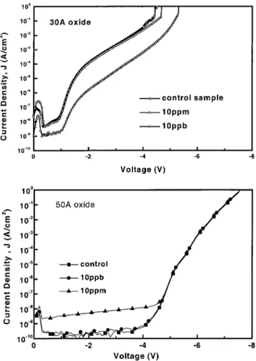
Figure 1a and b show the current density-voltage共J-V兲 charac-teristics of MOS capacitors with 30 and 50 Å oxides, respectively.
For the thick 50 Å oxide, the Cu contamination slightly increases the gate oxide leakage current in the pretunneling region, which may be attributed to the trap-assisted tunneling. The reason why the Cu contamination has little effect on the F-N tunneling may be due to a much larger current conduction than the trap-assisted tunneling at large bias. In contrast, a large leakage current is also observed in the direct tunneling region in addition to the increased pretunneling cur-rent. The two orders of magnitude larger leakage current at direct tunneling regime is unacceptable for low power circuit application. If a thinner oxide has a similar increasing trend for the leakage
zE-mail: [email protected]
Figure 1. J-V characteristics of MOS capacitors with共a, top兲 30 Å and 共b, bottom兲 50 Å oxides. The devices were contaminated by 10 ppb or 10 ppm Cu. A control sample without Cu contamination is also shown for comparison.
Journal of The Electrochemical Society, 148共4兲 F73-F76 共2001兲
0013-4651/2001/148共4兲/F73/4/$7.00 © The Electrochemical Society, Inc.
F73
) unless CC License in place (see abstract).
ecsdl.org/site/terms_use
address. Redistribution subject to ECS terms of use (see
140.113.38.11
current, then it will ultimately limit the gate oxide scaling because the allowed maximum leakage current is at 1 A/cm2.12
To further analyze the J-V characteristics, we have plotted the leakage current and breakdown electric field in Fig. 2a and b, re-spectively. As shown in Fig. 2a, the leakage current is one to two orders higher in the Cu-contaminated sample than in the control sample, and the leakage current generally increases with the Cu-contamination level. The higher leakage current of Cu-contaminated MOS devices than control samples suggests a higher defect density inside the oxide. According to the lattice-damage model, defects with a higher density in the oxide will grow faster and finally gen-erate a current conduction path that will have a very high energy density and cause oxide breakdown.13Therefore, the higher leakage current in Cu-contaminated samples is expected to correlated with a lower breakdown electric field. This is further evidenced from the lower cumulative breakdown field of Cu-contaminated samples shown in Fig. 2b, where the breakdown is defined at a current den-sity of 103A/cm2. It is important to notice that no such effect of lowering the breakdown field was found in the thick 50 Å oxide as shown in Fig. 1b and in agreement with the literature regarding low Cu contamination.1
Figure 3 shows the QBDdistribution of ultrathin⬃30 Å oxides. The standard oxide without contamination has a mean QBD of ⬃0.13 C/cm2at a constant voltage stress of⫺4.3 V, which is close to the data published in the literature.14The Cu-contaminated MOS capacitor has a larger QBDdistribution than the control device, and this is consistent with the larger distribution of leakage current and
the breakdown electric field shown in Fig. 2a and b. The larger QBD distribution might be due to a wide variation of the Cu concentration inside the oxide. In addition to the larger distribution, the Cu-contaminated MOS capacitor has a lower QBDvalue than the control device. The larger QBD distribution in combination with a lower QBDfor the capacitor contaminated with 10 ppm Cu than the one contaminated with 10 ppb Cu may be due to the higher Cu concen-tration inside the oxides.
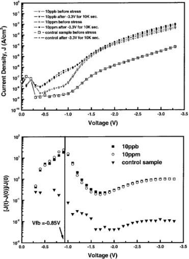
Figure 4. 共a, top兲 J-V characteristics of 30 Å oxides with different Cu con-tamination levels stressed at⫺3.3 V for 10,000 s and 共b, bottom兲 current change关J(t)-J(0)兴/J(0) plot of 共a兲 to enhance the stress effect.
Figure 2. 共a, top兲 The leakage current density and 共b, bottom兲 the break-down electric field of 30 Å oxides with different Cu contamination levels. The breakdown is defined at a current density of 105A/cm2共0.1 A through a 100⫻ 100 m area兲.
Figure 3. The QBDdistribution at⫺4.3 V constant voltage stress of ultrathin 30 Å oxides with different Cu contamination level.
Journal of The Electrochemical Society, 148共4兲 F73-F76 共2001兲 F74
) unless CC License in place (see abstract).
ecsdl.org/site/terms_use
address. Redistribution subject to ECS terms of use (see
140.113.38.11
We have also studied the SILC effect in these samples. Figure 4a shows the stress effect on the J-V characteristics. The stress condi-tion is⫺3.3 V for 10,000 s, which is equivalent to a total charge injections of 0.9 C/cm2 and ⬃45 C/cm2 for the control and Cu-contaminated devices, respectively. The constant voltage stress is used because it represents a more accurate stress condition for ul-trathin oxide than the constant current stress. Under the same stress conditions the control oxide shows the smallest current increase. We have plotted the current change关J共t兲-J共0兲兴/J共0兲 to further analyze the stress effect. As shown in Fig. 4b, the current change increases with increasing Cu contamination level, and the peak values are close to the flatband voltage measured by C-V. A similar result was also reported for ultrathin oxides without contamination16 and the mechanism was attributed to be the interface trap-assisted tunneling. The reason why there is no discernible peak in the control sample is ascribed to the very small current close to the noise margin of our measurement system.
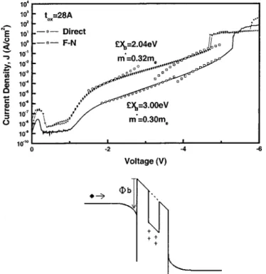
To study the cause of the large leakage current in the Cu-contaminated sample, we have analyzed the J-V characteristics us-ing theoretical direct and F-N tunnelus-ing equations.15 Figure 5a shows the theoretically calculated and measured J-V characteristics. Good matching between the measured and calculated J-V character-istics at direct and F-N tunneling regions can be obtained in the control MOS capacitor with a barrier height of 3.0 eV and an effec-tive mass of 0.30 me. These values are close to the data published in the literature.13The fitted oxide thickness of 28 Å is also close to the value measured by ellipsometry, which has an error of 6.7%. These results point out the good accuracy of the theoretical calculation. For the Cu-contaminated oxide, the best fitting result gives a barrier height and an effective mass of 2.04 eV and 0.32 me, respectively. The large error between the measured and calculated currents may be due to a spread of barrier height that cannot be modeled by a single fixed barrier height value. From the theoretically calculated J-V and the measured data, it is suggested that a barrier lowering exists in the Cu-contaminated oxide. Based on this result, we pro-pose a tunneling model in the Cu-contaminated ultrathin oxide as shown in Fig. 5b. It is known that the oxide charges or traps can
create a local energy variation inside the oxide,17 and we believe that Cu may have the same effect on the oxide. Therefore, electrons may see an effectively lower tunneling barrier as they tunnel through the oxide.
Figure 6 shows a secondary ion mass spectroscopy共SIMS兲 depth profile for the MOS structure. A strong Cu accumulation is observed in the poly-Si and gradually diffuses into the oxide. Although the diffusion into the oxide seems to be retarded by the amorphous structure of the oxide, Cu can still be found in the oxide. Further-more, the presence of Cu at the Si-oxide interface can also explain the large SILC observed in Cu-contaminated samples because of the increased interface-trap density.12The higher number of interface-trap states can help the current tunneling as the applied voltage is less than the flatband voltage. The higher Cu concentration at the oxide-Si interface is also suggested by the C-V measurement of a thick 50 Å oxide, where the interface trap density increased from 2⫻ 1010eV⫺1/cm2in the control oxide to ⬃ 2 ⫻ 1011eV⫺1/cm2 in the Cu-contaminated samples.
Conclusion
We have studied the gate oxide integrity of 30 Å ultrathin oxides. One to two orders of magnitude larger leakage current is observed in the pretunneling and direct tunneling region than in control devices, even at a low Cu contamination level of 10 ppb. In contrast, only the pretunneling current increase is found in thick 50 Å oxides with the same Cu level. Because of the increased leakage current, degrada-tion of the breakdown electric field and QBDare expected. The de-graded gate oxide integrity is due to the presence of Cu inside the oxide as measured by SIMS. The presence of Cu at the oxide-Si interface can also increase SILC because of the higher number of Cu-induced interface states.
Acknowledgments
This work is supported by the National Science Council of the R.O.C. under contract no. 2215-E-317-006 and NSC89-2721-2317-200. The technical support from National Nano Device Laboratory is gratefully acknowledged.
National Chiao Tung University assisted in meeting the publication costs of this article.
References
1. B. Vermeire, L. Lee, and H. G. Parks, IEEE Trans. Semicond. Manuf., 11, 232
共1998兲.
2. D. A. Ramappa and W. B. Henley, J. Electrochem. Soc., 146, 2258共1999兲. 3. T. Gravier, F. Braud, J. Torres, J. Palleau, A. Chantre, and J. Kirtsch,
Microelec-tron. Eng., 33, 211共1997兲.
4. P. Motte, J. Torres, J. Palleau, F. Tardif, and H. Bernard, Solid-State Electron., 43, 1015共1999兲.
Figure 5.共a, top兲 Theoretically calculated and measured J-V characteristics from Fig. 1a and共b, bottom兲 band diagram illustrating the Cu effect in the oxide.
Figure 6. SIMS profile of 30 Å oxides contaminated by with ppm Cu. The Al contact was removed before SIMS analysis.
Journal of The Electrochemical Society, 148共4兲 F73-F76 共2001兲 F75
) unless CC License in place (see abstract).
ecsdl.org/site/terms_use
address. Redistribution subject to ECS terms of use (see
140.113.38.11
5. Y. Shacham-Diamand, A. Dedhia, D. Hoffstetter, and W. G. Oldham, in
Proceed-ings of IEEE VMIC Conference, 109共1991兲.
6. T. Heiser, S. McHugo, H. Hieslmair, and E. R. Weber, Appl. Phys. Lett., 26, 3576
共1997兲.
7. A. Correia, D. Ballutaud, and J. L. Naurice, Jpn. J. Appl. Phys., 33, 1217共1994兲. 8. K. Hozawa, T. Itoga, S. Isomae, J. Yugami, and M. Ohkura, in Proceedings of
Symposium on VLSI Technology, 24共2000兲.
9. M. Inohara, H. Sakurai, T. Yamaguchi, H. Tomita, T. Iijima, H. Oyamatsu, T. Nakayama, H. Yoshimura, and Y. Toyoshima, in Proceedings of Symposium on
VLSI Technology, p. 26共2000兲.
10. A. Chin, B. C. Lin, W. J. Chen, Y. B. Lin, and C. Tsai, IEEE Electron Device Lett.,
19, 426共1998兲.
11. A. Chin, C. C. Liao, C. H. Lu, W. J. Chen, and C. Tsai, in Proceedings of
Sym-posium on VLSI Technology, 133共1999兲.
12. A. Chin, Y. H. Wu, S. B. Chen, C. C. Liao, and W. J. Chen, in Proceedings of
Symposium on VLSI Technology, 16共2000兲.
13. S. Wolf, Si Processing for the VLSI Era, Vol. 3, p. 457, Lattice Press, Sunset Beach, CA共1995兲.
14. Y. Taur and T. K. Ning, Fundamentals of Modern VLSI Devices, p. 106, Cam-bridge University Press, New York共1998兲.
15. P. E. Nicollian, M. Rodder, D. T. Grider, P. Chen, R. M. Wallace, and S. V. Hattangady, in Proceedings of International Reliability of Physics Symposium, 400
共1999兲.
16. E. M. Vogel, K. Z. Ahmed, B. Hornung, W. Kirlen Henson, P. K. McLarty, G. Lucovsky, J. R. Hauser, and J. J. Wortman, IEEE Trans. Electron Devices, 45, 1350共1998兲.
17. Y. Taur and T. K. Ning, Fundamentals of Modern VLSI Devices, p. 85, Cambridge University Press, New York共1998兲.
Journal of The Electrochemical Society, 148共4兲 F73-F76 共2001兲 F76
) unless CC License in place (see abstract).
ecsdl.org/site/terms_use
address. Redistribution subject to ECS terms of use (see
140.113.38.11