Transient Device Simulation of Floating Gate
Nonvolatile Memory Cell With a Local Trap
Hiroshi Watanabe
Abstract—The single-electron general-purpose device simulator is improved to carry out a wide-range transient analysis from 1 ps to 10 years. We apply this simulator to a floating gate (FG) nonvolatile memory cell in order to simulate a degradation mode of data retention owing to the direct tunneling enhanced by the fixed charge stored by a local trap in an interpoly dielectric. The scaling impact of ideal high-K interpoly dielectric FG nonvolatile memory cell is also investigated.
Index Terms—Coulomb oscillation, device modeling, device simulation, floating gate (FG), local trap, memory, modeling, single-electron sensitivity, TCAD, trap-assisted tunneling.
I. INTRODUCTION
T
HE DESIGN window of a floating gate (FG) memory cell is narrowed by a local trap in dielectrics surrounding the FG because the trap causes data retention degradation, thresh-old voltage (VTH) dispersion, the increase of noise, and other disturbing effects. These influences become more notable with aggressive device scaling. Since hopping of electron modulates potential profiles around the traps, the operation of such a memory cell is sensitive to the single-electron hopping via the trap, which is similar to a Si dot surrounded by SiO2 [1]. On the other hand, a single-electron transistor composed of a Si dot may be regarded as a promising candidate at the final stage of complementary metal–oxide–semiconductor scaling [2]. The further scaling therefore results in a molecular transistor (e.g., single-C60 transistor [3]). It is noted that the local trap is much smaller than a Si dot and C60, whose diameters are several nanometers and 8 Å, respectively. Since the single-electron effect is enhanced as islands capturing single-electrons are made smaller, this effect is an intrinsic issue in current electron devices involving a local trap. The single-electron sensitivity in calculation is accordingly indispensable to demonstrate a trap–detrap phenomena. However, in the modeling, the band structure of the Si dot should be replaced with the trap levels that can be estimated by individual experiments. In the case of SiN film, Maruyama and Shirota studied transient leakage current through a stacked film of SiO2 and Si3N4 under the stressing, and then found that there are two different decay Manuscript received November 24, 2009; revised May 13, 2010; accepted May 14, 2010. Date of publication June 14, 2010; date of current version July 23, 2010. The review of this paper was arranged by Editor D. Esseni.The author was with the Advanced LSI Technology Laboratory, Toshiba Corporation, Yokohama 235-8522, Japan. He is now with the Department of Electrical Engineering and Microelectronics and Information Systems Re-search Center, National Chiao Tung University, Hsinchu 300, Taiwan (e-mail: [email protected]; [email protected]).
Color versions of one or more of the figures in this paper are available online at http://ieeexplore.ieee.org.
Digital Object Identifier 10.1109/TED.2010.2051248
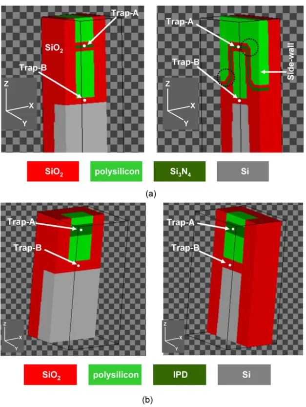
modes in the transient leakage current through the oxide from SiN film [4]. Assuming that the traps in SiN film have two relevant levels according to Robertson and Powell [5], they concluded that the upper level causes fast mode, and the other causes slow mode. From the fitting of the transient leakage current, it is found that the upper level is 1.2 eV lower than the conduction band edge of SiN film, and the lower level is a further 0.8 eV lower [4]. Such local traps are located in dielectrics of memory cell, as illustrated in Fig. 1(a), for example. Trap-A is located at the center of SiN film between oxides (ONO) and Trap-B is located at the center of tunnel oxide (TOX) between the FG and the Si substrate (SUB). The ONO film between the FG and the control gate (CG) is also called an interpoly dielectric (IPD).
Considering the freedom of spin, we have five charge states of (+2), (+1), (0), (−1), and (−2), where the state of (+2) has no electron, that of (+1) has an electron in bottom level, that of (0) has two electrons in bottom level and the charge neutrality, that of (−1) has an electron in upper level and two electrons in bottom level, and that of (−2) has two electrons in upper level and two electrons in bottom level. These charge states are transited among them owing to the hopping of electrons, as illustrated in Fig. 2 [Trap-A in (a) and Trap-B in (b)]. In the upper lines of Fig. 2(a) and (b), a positive bias is applied on the CG, while a negative bias is applied in the bottom lines of Fig. 2(a) and (b). Since the transition via trap is associated with the applied bias condition as well as charge state of trap, it is complicated to describe it at all the charge states. In order to make it simple, let us consider the state of (0) in the upper line of Fig. 2(a) at positive CG bias condition. If an electron is injected from the left electrode to the upper level of trap, the charge state is transited to the state of (−1) and the self-potential of trap becomes shallow (upward in energy diagram), which enhances the emission of the electron from the upper level to the right electrode and suppresses the injection of another electron from the left electrode. If the emission rate to the right becomes larger than the injection rate from the left at the state of (−1), an electron can be emitted from the upper level to the right and then the self-potential becomes deep (downward in energy diagram), which makes the state of (0) again. It is noted here that the electron injected from the left electrode to the upper level of the trap at the state of (0) loses energy that compensates the energy discrepancy between the injecting electron energy and the self-potential level of trap after the electron is injected. The process in which this energy loss is negative must be prohibited without any activation due to thermal (phonon) process, alpha ray, neutron ray, and so on. If the energy loss is positive, the electron transition is inelastic 0018-9383/$26.00 © 2010 IEEE
1874 IEEE TRANSACTIONS ON ELECTRON DEVICES, VOL. 57, NO. 8, AUGUST 2010
Fig. 1. Simulation sample of FG-memory cell with Trap-A in ONO layer and Trap-B in TOX. At y–z plane in (a), the circled portions increase the number of meshing points substantially.
trap-assisted tunneling, and the positive energy loss may be considered as absorbed by phonon-motion. If the energy loss is zero, the transition is elastic trap-assisted tunneling. In any event, the electron is considered to be transported from the left electrode to the right one via the upper level by trap-assisted tunneling [6]–[10] as long as the energy loss is not negative. If an electron is transported via the bottom level, the energy loss is increased by 0.8eV, which is equivalent to the energy discrepancy between the upper and the bottom levels.
If the emission and the injection rates were the same at the state of (−1), it would be stable. Generally speaking, local traps are so small that single-electron potential change is large enough to break the detailed balance where the emission and the injection rates are the same. If the detailed balance exists between the states of (−1) and (0), an electron can be emitted from the upper level to the right electrode at the state of (−1), and the charge state is then transited to (0), while another electron can be injected into the upper level at the state of (0),
Fig. 2. Hopping transport via local trap in TOX [Trap-A in (a) and Trap-B in (b)]. and the charge state is then transited to (−1) as long as the energy loss is not negative. Where the detailed balance exists is determined by the bias condition. If the positive bias is smaller, the detailed balance exists between the states of (0) and (+1). If the positive bias is even smaller, the detailed balance exists between the states of (+1) and (+2). If the positive bias is still smaller, the detailed balance exists out of the state of (+2) and then we have no recursive trap-assisted tunneling, which is described in Section III. In a case of negative bias, the above discussion can be extended to the opposite direction, as shown in the bottom lines of Fig. 2(a) and (b). In this way, we found that the trap–detrap process makes the self-potential of local trap oscillate around the detailed balance point between two adjacent charge states, which is determined by electric field across dielectric layer involving local trap, as long as the energy loss is not negative. If an electron is transported via trap, it is recursively pumped up to result in the hopping transport [1].
It is also noted that the volume of the local trap is too small for us to define the capacitance couplings around the trap. We, then, need a solver that is sensitive to single-electron potential change due to trap–detrap phenomena. On the other hand, data retention is a long-term transient phenomenon, e.g., 10 years, although a typical period of trap–detrap phenomena is much shorter. To study such a long-term transient single-electron oscillation, we have to improve the general-purpose device simulator that has single-electron sensitivity in computation, which is demonstrated in [1].
In this paper, we demonstrate the single-electron device simulation that enables us to study advanced modeling of the local trap issue in an FG memory cell. In Section II, we describe the calculation method. The results obtained are shown in
Section III. Sections IV and V are devoted to the discussion and the conclusion, respectively.
II. CALCULATIONMETHOD
As mentioned above, local traps are small and not connected to any electrode defining a boundary condition of potential profile there. We, however, have already resolved this problem in the case of a Si dot [1], using a self-consistent recursion method with highly precise physical models [11]–[16]. On the other hand, it should be noted that an end-point of a tunnel path associated with a trap cannot be integrated within 2-D k-space perpendicular to tunnel path. To calculate emis-sion and injection rates, we apply the WKB approximation [17]–[19] with a given wavenumber along tunnel path, kx,
regarding trap levels as the other wave number, kt. This means
that the summation of ktis replaced with that of local traps in
Harrison’s formula described in [11, eq. (9)]. Accordingly, we have five basic steps to simulate this, namely: 1) to calculate the profiles of carriers and potential while achieving the single-electron sensitivity in calculation; 2) to search a tunnel path in a 3-D simulation sample at a given profiles of carriers and potential at the last step; 3) to calculate the tunnel hopping of electron along the searched paths at the last step; 4) to obtain the elapsed time during the tunneling; and 5) to turn to the first step until the cumulative elapsed time is attained at a predetermined time. It is noted that we cannot trace the revision in these profiles due to the tunnel hopping without the single-electron sensitivity in calculation.
We regard SiO2 and Si3N4 as large-gap and low-K semi-conductors, e.g., EG = 8.95 eV [20] and K = 3.9 [21] in SiO2
1876 IEEE TRANSACTIONS ON ELECTRON DEVICES, VOL. 57, NO. 8, AUGUST 2010
and EG = 5.4 eV [22] and K = 7.5 [21] in Si3N4, while EG = 1.12 eV [21] and K = 11.7 [21] in silicon and polysilicon, where EG and K depict energy gap and dielectric constant, respectively. The tunnel barriers for electrons are 3.34 eV and 2.38 eV in SiO2and Si3N4, respectively, since the valence-band affinities are 4.49 eV [23] and 1.9 eV [22] in SiO2and Si3N4, respectively.
A. Single-Electron Sensitivity in 3-D Device-Simulator A CG bias applied on the CG (VCG) is divided to the po-tential drops of the depletion layer at the CG bottom, the ONO layer, the accumulation layer at the FG top, the depletion layer at the FG bottom, TOX, and the inversion layer on the Si sur-face. The depletion layers at CG and FG bottoms are modeled considering the incomplete depletion layer with a phenomenon known as “surface band-gap narrowing” according to [14], since CG and FG are made of degenerate n+-polysilicon where the donor concentration is 1020cm−3in the present simulation sample. The accumulation layer at the FG top is narrow but not negligible in precise calculation, which is modeled according to [15] and [16]. The surface charge is thereby increased in proportion to band bending to the power of 3/4 [16], which is a phenomenon known as “weak accumulation.”
Other than the aforementioned incomplete depletion [14] and weak accumulation [15], [16], and the inversion layer on the Si surface, VCG is mainly divided to potential drops across TOX and ONO layers, which potential drops are determined by self-potential of the FG. It is, unfortunately, difficult to solve the self-potential of the FG that is not connected to any electrode, since it is a boundary value problem. This is similar to cases of a Si dot [1] and local traps. One might regard self-potential as Cr× VCG, where Cr is the capacitance coupling ratio defined by Cr = CONO/(CTOX+ CONO) with CONO being the capacitance between CG and FG, and CTOX being the capacitance between FG and SUB. However, the VTHmust be shifted by the stored charge that is individual from the capac-itance couplings. In other words, if this method was valid, Cr at programmed state would differ from that at erased state. How-ever, CTOX and CONO are independent of the stored charge. Therefore, this method is invalid. Even though the fringe ca-pacitance is considered, this method must be invalid because the fringe capacitance is also independent of stored charge. It is noted that the method, in which Cr is used as an adjustable parameter to individually fit the calculated characteristics of program and erase with the measurements, is invalid before the sample that will be measured is fabricated. Moreover, it is not appropriate for “general-purpose use” considering local traps and the Si dot as well as FGs. The Cr is an important index of device design and should not be used as a fitting parameter.
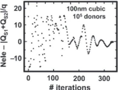
In order to catch potential shift due to stored charge, we have to study a detailed charge balance taking into consideration the number of stored electrons (Nele) and surface charges QS1
at the Si surface and QS2 at the CG bottom. Here, note that
we can regard Nele− |QS1+ QS2|/q as the computational
error that should be suppressed. In Fig. 3, we show the cal-culation result of the module implemented here to suppress the computational error, i.e., Nele− |QS1+ QS2|/q, where the
computational sample is a 100-nm cubic FG with the doping
Fig. 3. Single-electron sensitivity in calculation leakage current between calculation and measurement.
concentration of phosphorus being 1020cm−3, i.e., 105donors therein. After the conventional solver is converged, the residual error is decreased with the iteration of the present module and then vanishes. In this way, the present general-purpose 3-D device-simulator achieves an amazing precision that can detect the single-electron modulation in potential profile, so-called “single-electron sensitivity in computation” [1].
B. To Search Tunnel Paths
At a given potential profile, in order to search the tunnel paths used for calculating tunnel fluxes, we search whole the 3-D simulation sample comprised of local traps, CG, FG, SUB, IPD, and the oxides surrounding the FG, as shown in Fig. 1(a) and (b). In this search, we regard each trap as a 2-Å cubic semi-conductor cluster and then divide it with 20× 20 × 20 meshing points. Other semiconductor regions are FG (polysilicon), CG (polysilicon), and SUB (silicon). These semiconductor islands are isolated from one another by oxides or IPD, and accordingly the surfaces surrounding isolated islands are not connected. Each surface consists of the surface elements that are cut out by a boundary surface from a control volume at the surface. Next, we connect two of these surface elements that belong to isolated islands with a straight line. Dividing, further, SUB to 3 islands of source, drain, and channel according to the doping profile, we can group the lines (tunnel paths) according to associating islands and then take the groups connecting Trap-A and CG, Trap-Trap-A and FG, Trap-B and FG, Trap-B and source, Trap-B and drain, Trap-B and channel, CG and FG, CG and source, CG and drain, FG and source, FG and drain, and FG and channel. In the present search, we have omitted the band-to-band tunneling through p–n junction, i.e., the paths across the boundary between channel and source–drain diffusion layer. Furthermore, we have prohibited the paths that are interrupted by a third semiconductor island. For example, a path is prohib-ited between CG and channel because it is interrupted by FG.
We also have to take into account the energy band diagram while searching the tunnel paths. Let us depict E as the energy of electron at the initial point of tunnel path. If a given E is less than EC or trap level at the end of tunnel path, the
considered path is prohibited. If we prevent the negative energy-loss process during tunneling, we also prohibit the paths where the energy of final state after tunneling is higher than E. In other words, if the end-point of tunneling is a trap, E must be larger than the trap level that will be updated owing to injection of an electron after the considered tunneling process. It appears that this can be regarded as the Coulomb blockade effect of local trap, which we will not considered explicitly because the
Fig. 4. Comparison of leakage current between calculation and measurement. description of capacitance surrounding trap is unknown. If the end-point is an FG, the potential change due to single-electron injection is negligibly small. If we take into consideration hopping processes of negative energy loss, we may recognize that some kind of activation is involved in the process. We can perform the simulation with and without a negative energy loss process, in order to investigate the impact of activation via local trap. Since the trap has bistate levels in the present modeling, we must judge the energy losses via upper and lower levels, respectively. We may consider that the positive energy loss is diffused by a phonon process that is not involved in the present simulation. Moreover, in order to make the simulation simple, we ignore the hole tunneling paths.
C. To Calculate Tunnel Flux
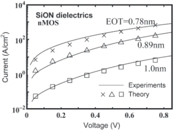
At each path we take into consideration two waves of going and coming that have opposite signs and then add their fluxes to obtain the net tunneling flux that we call “tunnel flux” below. We can thereby calculate the tunnel flux along the remaining tunnel paths assuming the 1-D WKB-based formula for calculating tunneling probability along each tunnel path (straight line). To confirm the validity of the present calculation, in Fig. 4, the calculated leakage current of n+-polysilicon/ SiON/p-Si capacitor is compared with the measured data pub-lished in [24]. The measured samples were analyzed using the AR-XPS method [25] to obtain the profile of local traps made of Si-N bond broken with an estimated dangling-bond yield [24]. This profile is also used in the calculation of current shown in Fig. 4. The tunnel mass is assumed to be 0.85m0, where m0is the rest electron mass, assuming the interfacial transition layer where EG and K are gradually changed [24], [26]. We have good agreements in samples of three different thicknesses, in which the effective oxide thickness (EOT) is 0.78 nm, 0.89 nm, and 1.0 nm. The same physical models are all implemented in the present 3-D device simulator.
We carry out the energy integration of these paths according to Harrison’s formula [11] and then obtain the distribution of tunnel fluxes over the tunnel paths connecting two isolated islands.
D. To Calculate Elapse of Time
Subsequently, we carry out the time integration of these tunnel paths until one of them reaches the elementary charge,
q, firstly, whereas the elapse of time during the first single-electron hopping is obtained. In other words, we can calculate the elapse of time while an electron is moved from one island to another through the path in which the time integrated flux reaches q firstly. In order to reproduce reduction of wave packet, we refresh (unset) all the tunnel fluxes calculated at the past steps of calculation. To satisfy Kirchhoff’s current law, the obtained tunnel flux from an island to another is subtracted from the current flowing in the former island and added to the current flowing in the other island. The 3-D device simulation is carried out again, using the distribution of electrons that is revised owing to single-electron hopping across the considered path. This is why the single-electron sensitivity in calculation is needed. This simulation is iterated until the convergence is obtained at each revision of profiles of potential and carriers and continued until the cumulative elapse of time is attained at the predetermined time.
We self-consistently implement this module and the afore-mentioned high-precision physical models to the long-term transient device simulator that was used to study the theoretical limitation of TOX thickness for 10 years data retention [27]. In addition, considering the fastest mode in operation, we must adjust the time slice in calculation so that it is shorter than the shortest characteristic time. As a result, the present device simulator exhibits the picosecond resolution in timing while achieving 10 years long-term transient analysis with single-electron sensitivity in computation.
E. Other Remarks in Calculation Method
If a double-path process from an island to a trap and from the trap to another island occurs sequentially, this can describe the trap-assisted tunneling as long as the energy loss is not negative. The capture cross-section of trap is not explicitly considered in this paper. Instead, we can integrate the surface element of trap, which is defined as a 2-Å cubic semiconductor cluster divided to 20× 20 × 20 meshing points. The integrated area of 2 Å× 2 Å is equivalent to 4 × 10⁻¹⁶ cm2 in estimation of capture cross-section. If it is defined as half a whole surface of trap, it is equivalent to 1.2× 10⁻¹⁵cm2in estimation of capture cross-section.
In the present simulation, a local trap as well as an FG can be regarded as floating semiconductor islands that make it difficult to solve the potential profile while keeping the single-electron sensitivity in calculation. Since it is further difficult to perform the simulation with three floating islands, i.e., two local traps and an FG, we consider either Trap-A or -B in the following simulation (not both).
It is also noted that the traps are located at the center of TOX and IPD layers, as shown in Fig. 1(a) and (b), since it becomes more difficult to obtain the single-electron sensitivity in calculation if the position is apart from the center.
Generally speaking, the tunnel path may not be a straight line. However, since we still have no idea how to determine the curved path appropriately in 3-D general-purpose device simulation, we assume the tunnel path is a straight line in this paper. This ignores the paths from the sidewall of ac-tive area to FG, which may cause a minor contribution at
1878 IEEE TRANSACTIONS ON ELECTRON DEVICES, VOL. 57, NO. 8, AUGUST 2010
Fig. 5. Applied voltage pulse on CG and drain.
most. We leave the influence of such curved paths for future study.
III. RESULTS
As shown in Fig. 1(a), we have a side-wall structure sur-rounding the FG to increase a capacitance coupling ratio [28] in the actual memory cell. However, the curved portion of side-wall requires more detailed mesh, which causes the in-crease of computational resources. Since a local trap requires 20× 20 × 20 meshing points, as mentioned above, we need to decrease the excess meshing points increased by the curvature of side-wall. We, thereby, simplify the device structure, as shown in Fig. 1(b). That is, to compensate the lack of the contribution from the side-wall to the capacitance coupling, we have replaced the ONO film with the IPD film of K = 15.6, whose EOT is 3.43 nm and TOX thickness is 10 nm so that we have Cr = 0.745. The tunnel barrier of IPD film is 3.34 eV/2.38 eV/3.34 eV. If a tunnel path across IPD film is parallel to z-axis, the length of the considered tunnel path is 4.6 nm/4.5 nm/4.6 nm. We have considered all the tunnel paths nonparallel to as well as parallel to z-axis in 3-D space. Trap-A and -B have bistate levels, 1.2 eV and 2.0 eV from the conduction band edge of the center of IPD film and TOX film, respectively. We have assumed that Trap-B has the same level structure as Trap-A, to make the discussion transparent.
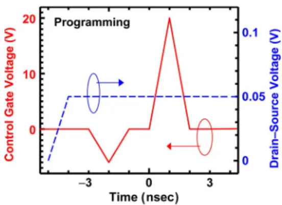
At the initial state, we gave four electrons to a trap, which artificially makes a nonequilibrium state, (−2). The transient device simulation was carried out in cases with no trap, with Trap-A, and with Trap-B. The pulse applied on CG and drain is shown in Fig. 5. The drain voltage is increased from 0 to 0.05 V with the elapse of time from−5 to −4 ns, and after that it is fixed. It is noted that the drain voltage of 0.05 V is too small to have an influence on data retention characteristics, as reported in [27]. The VCGsweeps between 0 and−6 V from −3 to−1 ns before programming. After a 1-ns interval, it sweeps again between 0 and 20 V from 0 to 2 ns, and the cell is then programmed. The source and substrate are grounded.
Let us prohibit the hopping process with negative energy loss via Trap-A, as mentioned in Section II. Fig. 6 is the calculation result of I–V characteristics, in which the data were plotted with respect to VCG-pulse from −2 to 2 ns in Fig. 5. That is, the VCG is increased from −6 to 20 V, and is then decreased to 0 V. Many electrons are injected from the channel to FG around 1 ns at which VCG is 20 V. This
Fig. 6. Simulated current–voltage characteristic.
Fig. 7. Simulated stored charge at Trap-A over time.
causes the threshold voltage shift (ΔVTH) that is defined as the discrepancy in VCG at 1 nA between before and after programming. As a result, we have ΔVTH= 3.4 V irrespective of Trap-A. This means that a local trap in the IPD layer has a negligible impact on the programming characteristic, which may be because the trap-assisted tunneling does not occur via Trap-A during programming. In Fig. 7, it is shown that the one-by-one emission occurs in scale of 0.1 ns before the saturation (+2) occurs at 0.4 ns, whereas we have no oscillation after Trap-A is saturated at (+2). This means that the electric field across IPD layer is so low owing to a large Cr(= 0.745) that the energy level of tunneling electron is lower than the bottom-level of Trap-A. Then, we have a fixed positive charge in the IPD layer. The IPD leakage via Trap-A is therefore regarded as the direct tunneling enhanced by barrier lowering due to the fixed positive charge stored by the trap, as illustrated in Fig. 8. This is similar to the leakage mechanism through ultrathin gate SiON dielectrics [24]. In Fig. 9, shown are the calculation results of the number of stored electrons in the FG and the drain current over time, in which the number of stored electrons is drastically decreased at 4.7 months (≈1.5 × 10⁷ s) with Trap-A whereas it is unchangeable during 10 years (3× 10⁸s) without Trap-A. It is shown that the current begins to flow at 4.7 months with Trap-A whereas it does not during 10 years without Trap-A, which is consistent with the number of stored electrons. It is thereby found that the retention characteristics of the FG memory cell are substantially degraded owing to fixed positive charge at a local trap in IPD layer.
During the standby, the electric field across TOX is so weak that Trap-B has less impact on data retention. We therefore
Fig. 8. Band-profile around Trap-A in retention state.
Fig. 9. Retention characteristics of the number of stored electrons and drain current: the insertions show that the number of stored electrons is decreased to be the same with that of stored electrons without trap when the drain current is increased to 1 nA.
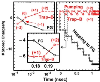
removed Trap-B from the long-term plot. In order to investigate the short-term impact of Trap-B, we reduce TOX thickness from 10 to 3.2 nm, which is equivalent to the theoretical limitation for 10 years data retention with no trap [27], and the EOT of IPD layer from 3.34 to 2.14 nm, so that the capacitance coupling ratio is 0.6, still larger than 0.5. We, further, include the process of negative energy loss via Trap-B, in which the limitation is−1.5kBT with kB being the Boltzmann constant
and T being temperature, 300 K. The calculation result of charge states is shown in Fig. 10, while VCG is fixed to be 6 V. With the elapse of time, the excess electrons artificially given at the initial state are all emitted up to 6 ps, which results in (+2). Although it might be shown in the broken circle that the hopping of double electrons occurs at the same time, the insertion clearly suggest the one-by-one hopping. An electron passes through Trap-B from the channel to FG while the trap state is (+1). Another electron is transferred from the bottom level of Trap-B to FG while the charge state is transited from
Fig. 10. Simulated stored charges at Trap-B over time.
(+1) to (+2). It is noted that the phase and period of oscillation between (+1) and (+2) agree with the hopping of the electron to the FG, which suggests that such an iterative pumping can be regarded as the trap-assisted tunneling and causes the overpro-gramming. After 1 ns, the oscillation of Trap-B is continued while the number of stored electrons in FG is unchanged. This means that electron comes and goes between Trap-B and channel. On the other hand, if we remove the process of negative energy loss via Trap-B from the simulation, this oscillation after 1 ns vanishes. It is thus suggested that the recursive hopping between Trap-B and channel is caused by an energy gain from thermal or other activation. Since the oscillation before 1 ns is left, the trap-assisted tunneling can occur without the negative energy loss. It is also found in the insertion that the time resolution of the present simulator reaches the order of 1 ps.
To demonstrate usefulness of this simulator further, in Fig. 11, we show the simulation result of a 3-D sample having pure oxide IPD and side-wall, which is made by replacing Si3N4layer with SiO2layer in Fig. 1(a). Here, we assumed no trap condition that enables us to simulate this side-wall structure because the meshing points are substantially reduced. At the first row, the applied pulses are shown. First, an erase pulse of −24 V is applied on CG, and, subsequently program pulses of 16 V, 18 V, 20 V, 22 V, and 24 V are applied. A drain voltage of 1 V and read pulse of −6 V/+6 V are iteratively applied during each standby between program pulses. At the second row, we show the simulation result of electric fields across TOX and the pure oxide IPD layers. The currents across TOX and the pure oxide IPD layers are shown at the third row. It is found that the electric fields and the currents are changed for recovering the detailed balance, at which the currents and fields across TOX and IPD layers are the same, during program. At the last row, we show the simulation result of stored charge in the FG. The sequential programs increase the number of stored electrons step by step, after erasing. Next, we replace the pure oxide IPD by the ONO layer, in which a 10-nm nitride layer is sandwiched between two oxides of 2 nm, 3 nm, and 4 nm. The resultant simulation samples have the side-wall surrounding the FG with no local trap. The simulated VTH shift is increased
1880 IEEE TRANSACTIONS ON ELECTRON DEVICES, VOL. 57, NO. 8, AUGUST 2010
Fig. 11. Simulation result of pure oxide IPD cell whose structure is shown in Fig. 1(a).
Fig. 12. Comparison of simulated relative VTHshifts after programming the
pulse shown in Fig. 11.
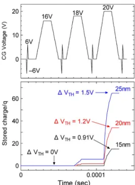
with the decrease of oxide thickness, as shown in Fig. 12. For comparison, we also show the simulated VTH shift of sample having pure high-K IPD (K = 25 and tunnel barrier is 1.08 eV1) and the same structure with Fig. 1(b) (with no side-wall) at the right end. The resultant VTH shift is even larger in cell of pure high-K IPD, which means that a pure high-K IPD has a significant advantage in multibit cell beyond 30-nm generations. Subsequently, we show the scaling trend of such pure high-K IPD cell (with no side-wall) from 25 to 15 nm in Fig. 13. We have assumed a very shallow diffusion layer (Xj =
5 nm) for improving the simulated ID–VD characteristics,
even though the manufacturing solution is still not known, and thereby obtained the simulated VTH shift. The simulated VTH shift after a 20-V pulse is decreased from 1.5 V, 1.2 V, and 0.91 V as the scaling is advanced. The number of stored
1See Appendix.
Fig. 13. Simulated scaling impact of pure high-K cell whose structure is shown in Fig. 1(b).
electrons is also decreased in a similar manner, 65, 34, and 15. This may be due to the fact that the fringe capacitance is dominating the capacitance coupling ratio with the scaling. In Fig. 14, we plot the scaling dependency of VTHshift per stored electron with pure high-K cell. This value is larger than thermal energies at room temperature and 85◦C at 25 nm and 20 nm, respectively, which suggests that single-electron nonvolatile memory cell is hopeful far beyond 20-nm generations as long as pure high-K IPD can be fabricated on cubic FG.
Fig. 14. Simulated scaling impact of VTHshift due to a stored electron.
The cell-to-cell space is also shrunk in memory cell arrays, which makes the side-wall control difficult and enhances the cell-to-cell crosstalk. However, if the height of FG is shrunk with the scaling, the cell-to-cell capacitance coupling can keep unchangeable during the scaling. The improvement of junction is indispensable to take advantage of high-K FG memory cell.
IV. DISCUSSION
From the literature [9], [10], it is reported that the retention degradation is due to stress-induced leakage current caused by trap-assisted tunneling. However, we consider that the degrada-tion mechanism is comprised of several components of leakage current through the IPD layer in actual memory cell. In this paper, using 3-D device simulation, we showed a possibility that fixed charge can also degrade the data retention character-istics. Provided that negative energy loss process is prohibited in calculation of tunnel fluxes, the energy of tunneling electron must be higher than the trap level that will be updated after the considered tunneling. Since the trap level is raised by the injection of electron, a very deep level is needed to make the energy loss nonnegative for exhibiting the trap-assisted tunnel-ing through IPD film. A large capacitance coupltunnel-ing ratio also decreases the electric field across the IPD layer, and then the possibility of trap-assisted tunneling is suppressed. Of course, in a large gate area sample, there may be a broad distribution of trap levels, some of which are deep enough to exhibit the trap-assisted tunneling. However, in a very small gate area cell (e.g., 30 nm× 30 nm), there may be a delta-like distribution of trap-level (e.g., twin delta for bi-states in this work) because a trap per 30 nm× 30 nm area is equivalent to 1.1 × 1011cm−2. The surface density of interfacial trap (Dit) of MOS capacitor is typically 1010 cm−2. Since the oxidation process has been improved through the history of the development of MOSFET, Dit is rather low in MOS capacitor. We may thus regard trap density as much higher in IPD film than in MOS capacitor, i.e., tenfold in this work. Although it still appears that 1.1× 1011 cm−2 is rather low compared with [4], the IPD process may have been improved these 15 years. In addition, we have aimed the simulation of the leakage component that cannot be measured, as mentioned below. We, therefore, have regarded
Fig. 15. Relationship between tunnel barrier heights and dielectric constants. few traps as existing in a cell. Trap levels may differ among cells, and accordingly some cells have deep traps exhibiting trap-assisted tunneling and others can exhibit direct tunneling enhanced by fixed charge. It is noted that a very small cell may be different in physics from a large gate area sample that is convenient to measure stress-induced leakage current. It is difficult to measure the leakage current through IPD layer in such a small cell because it is too low. For example, the ITRS roadmap requires the leakage is less than 10−25A [29], which is hardly measurable. This clearly suggests a merit of simulation work in which empirical fitting parameters are removed as possible as we can.
In this paper, Trap-B has no impact on data retention of a 30-nm cell, since TOX thickness is 10 nm, which is much thicker than the ITRS requirement, i.e., 6–7 nm [29]. On the other hand, if TOX has no trap, the theoretical limitation of TOX thickness is 3.2 nm for 10 years data retention in a 30-nm cell without any trap [27]. Since the leakage current is the maximum when a trap is located at the center of insulating film, 6.4 nm, at least, is required for 10 years data retention. This consists with the ITRS requirement [29].
V. CONCLUSION
We improved a general-purpose single-electron device sim-ulator to carry out a wide-range transient analysis from 1 ps to 10 years. It is found that the data retention of an FG memory cell can be degraded from 10 years to less than 5 months with a local trap in IPD layer, in which the leakage mechanism can be regarded as the enhancement of direct tunneling due to the fixed positive charge stored by the trap. This is similar to the intrinsic degradation mechanism of SiON gate dielectric [24]. It is also found that a local trap in TOX may cause trap-assisted tunneling from channel to FG, and the cell is then overprogrammed. The potential of the present device simulator is promising for the study of scaling impact of FG memory cells.
APPENDIX
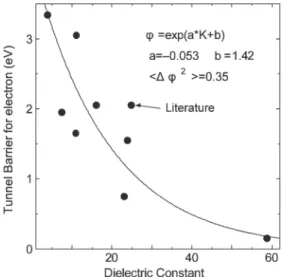
In Fig. 15, we regulate the data of tunnel barriers and dielectric constants according to [21]–[23], and [30]. Using an
1882 IEEE TRANSACTIONS ON ELECTRON DEVICES, VOL. 57, NO. 8, AUGUST 2010
exponential function, we can plot an empirical curve on the graph within fit variance being 0.35. If we regard the dielectric constant as 25, which may be equivalent to a La–oxide, this empirical curve indicates that the tunnel barrier is 1.08 eV. The barrier height is so low that trap-assisted tunneling may be a major cause of data retention degradation if there is a trap in this IPD film.
ACKNOWLEDGMENT
The author would like to thank T. Maruyama and H. Inoue for their encouraging this work. The present program was coded adding the modules for the single-electron sensitivity in calculation and the very wide range transient analysis to the do-mestic device-simulator that Toshiba Semiconductor Company developed. The author would like to thank A. Fathurahman and D. Hagishima for their fixing bug of the source code and D. Matsushita for supplying the measured data of tunnel current shown in Fig. 3. In addition, the author changed the affiliation from Advanced LSI Technology Laboratory, Toshiba Corporation, Yokohama, Japan to Department Elec. Eng. and Microelectronics and Information Systems Research Center, National Chiao Tung University, Hsinchu, Taiwan.
REFERENCES
[1] H. Watanabe, “Hopping transport of electrons via Si-dot,” in Proc.
SISPAD, Vienna, Austria, 2007, pp. 249–252.
[2] K. Uchida, J. Koga, R. Ohba, and A. Toriumi, “Room-temperature oper-ation of multifunctional single-electron transistor logic,” in IEDM Tech.
Dig., 2000, pp. 863–867.
[3] H. Park, J. Park, A. K. L. Lim, E. H. Anderson, A. P. Alivistatos, and P. L. McEuen, “Nanomechanical oscillations in a single- C60transistor,” Nature, vol. 407, no. 6800, pp. 57–60, Sep. 2000.
[4] T. Maruyama and R. Shirota, “The low electric field conduction mech-anism of silicon oxide-silicon nitride-silicon oxide interpoly-Si di-electrics,” J. Appl. Phys., vol. 78, no. 6, pp. 3912–3914, Sep. 1995. [5] J. Robertson and M. J. Powell, “Gap states in silicon nitride,” Appl. Phys.
Lett., vol. 44, no. 4, pp. 415–417, Feb. 1984.
[6] D. J. Dimaria and E. Cartier, “Mechanism for stress induced leakage cur-rent in thin silicon dioxide films,” J. Appl. Phys., vol. 78, no. 6, pp. 3883– 3894, Sep. 1995.
[7] S. Takagi, N. Yasuda, and A. Toriumi, “Experimental evidence of inelas-tic tunneling in stress-induced leakage current,” IEEE Trans. Electron
Devices, vol. 46, no. 2, pp. 335–341, Feb. 1999.
[8] S. Takagi, N. Yasuda, and A. Toriumi, “A new I– V model stress-induced leakage current including inelastic tunneling,” IEEE Trans. Electron
Devices, vol. 46, no. 2, pp. 348–354, Feb. 1999.
[9] D. Ielmini, A. Spinelli, M. A. Rigamonti, and A. L. Lacaita, “Modeling of SILC based on electron and hole tunneling—Part I: Transient effects,”
IEEE Trans. Electron Devices, vol. 47, no. 6, pp. 1258–1265, Jun. 2000.
[10] L. Larcher, A. Paccagnell, and G. Ghidini, “A model of the stress induced leakage current in gate oxide,” IEEE Trans. Electron Devices, vol. 48, no. 2, pp. 285–288, Feb. 2001.
[11] W. A. Harrison, “Tunneling from an independent-particle point of view,”
Phys. Rev., vol. 123, no. 1, pp. 85–89, Jul. 1961.
[12] H. Watanabe and S. Takagi, “Effects of incomplete ionization of impu-rities in poly-Si gate and band gap narrowing on direct tunneling gate leakage current,” J. Appl. Phys., vol. 90, no. 3, pp. 1600–1607, Aug. 2001.
[13] H. Watanabe, K. Matsuzawa, and S. Takagi, “Scaling effects on gate leakage current,” IEEE Trans. Electron Devices, vol. 50, no. 8, pp. 1779– 1784, Aug. 2003.
[14] H. Watanabe, “Depletion layer of gate poly-Si,” IEEE Trans. Electron
Devices, vol. 52, no. 10, pp. 2265–2271, Oct. 2005.
[15] H. Watanabe, K. Nakajima, K. Matsuo, T. Saito, and T. Kobayashi, “Re-duction of accumulation thickness in metal gate,” in Proc. Abs. SSDM, 2005, pp. 504–505.
[16] H. Watanabe, K. Matsuo, T. Kobayashi, K. Nakajima, and T. Saito, “Weak accumulation of gate polysilicon,” in Proc. 11th IWCE, 2006, pp. 89–90. [17] V. G. Wentzel, “Eine Verallgemeinerung der quantenbedingu ugen fur die
Zeeckeder wellenmechanik,” Z. Physik, vol. 39, pp. 518–529, 1926. [18] H. A. Kramers, “Wellenmechanik und halbzahlige quantisierung,”
Z. Physik, vol. 39, no. 10/11, pp. 828–840, Oct. 1926.
[19] L. Brillouin, “Lamecanique ondulatire de Schrodinger,” Compt. Rend., vol. 183, pp. 24–27, 1926.
[20] S. Miyazaki, H. Nishimura, M. Fukuda, L. Leyb, and J. Risteinb, “Struc-ture and electronic states of ultrathin SiO2 thermally grown on Si (100) and Si(111) surfaces,” Appl. Surf. Sci., vol. 113/114, pp. 585–589, Apr. 1997.
[21] S. Sze, Physics of Semiconductor Devices. Hoboken, NJ: Wiley, 1981. [22] S. Miyazaki, M. Narasaki, A. Suyama, M. Yamaoka, and H. Murakami,
“Electronic structure and energy band offsets for ultrathin silicon nitride on Si (100),” Appl. Surf. Sci., vol. 216, no. 1, pp. 252–257, Jun. 2003. [23] J. L. Alay and M. Hirose, “The valence band alignment at ultrathin
SiO2/Si interfaces,” J. Appl. Phys., vol. 81, no. 3, pp. 1606–1608, Feb. 1997.
[24] H. Watanabe, D. Matsushita, K. Muraoka, and K. Kato, “Universal Tunnel Mass and Charge Trapping in [(SiO2)1−x(Si3N4)x]1−ySiyFilm,” IEEE Trans. Elec. Dev., vol. 57, no. 5, pp. 1129–1136, May 2010.
[25] K. Muraoka, K. Kurihara, N. Yasuda, and H. Satake, “Optimum structure of deposited ultrathin silicon oxynitride film to minimize leakage current,”
J. Appl. Phys., vol. 94, no. 3, pp. 2038–2045, Aug. 2003.
[26] H. Watanabe, D. Matsushita, and K. Muraoka, “Determination of tun-nel mass and physical thickness of gate oxide including poly- Si/SiO2
and Si/SiO2interfacial transition layers,” IEEE Trans. Electron Devices,
vol. 53, no. 6, pp. 1323–1330, Jun. 2006.
[27] H. Watanabe, T. Ishihara, Y. Matsunaga, K. Matsuzawa, D. Matsushita, and K. Muraoka, “Numerical study of data retention due to direct tunnel-ing for nonvolatile memory cell,” IEEE Trans. Electron Devices, vol. 52, no. 5, pp. 955–961, May 2005.
[28] S. Aritome, S. Satoh, T. Maruyama, H. Watanabe, S. Shuto, G. J. Hemink, R. Shirota, S. Watanabe, and F. Masuoka, “A 0.67um2 self-aligned shal-low trench isolation cell (SA-STI cell) for 3 V-only 256 Mbit NAND EEPROM,” in IEDM Tech. Dig., 1994, pp. 61–64.
[29] [Online]. Available: http://www.itrs.net/Links/2008ITRS/Home2008.htm [30] J. Robertson, “Band offsets of high dielectric constant gate oxide on
silicon,” J. Non-Cryst. Solids, vol. 303, no. 1, pp. 94–100, May 2002.
Hiroshi Watanabe was born in Gunnma, Japan.
He received the B.Sc., M.Sc., and Ph.D. degrees in physics from the University of Tsukuba, Tsukuba, Japan, in 1989, 1991, and 1994, respectively.
From 1994 to 2010, he was with the Corporate Re-search & Development Center, Toshiba Corporation, Yokohama, Japan. Since February 2010, he has been a tenure-track faculty Full Professor with the Depart-ment of Electrical Engineering and Microelectronics and Information System Research Center, National Chiao Tung University, Hsinchu, Taiwan. He has studied quantum-statistical mechanics, quantum spin systems, device physics and device modeling, and some cutting edge devices. His current research interest is to establish new device physics for the nanodevice era. He has over 150 patents all over the world (including under examination).
![Fig. 2. Hopping transport via local trap in TOX [Trap-A in (a) and Trap-B in (b)].](https://thumb-ap.123doks.com/thumbv2/9libinfo/7969378.158457/3.891.212.669.99.536/fig-hopping-transport-local-trap-tox-trap-trap.webp)