ECS Solid State Letters, 1 (2) R9-R12 (2012) R9 2162-8742/2012/1(2)/R9/4/$28.00©The Electrochemical Society
Photoluminescence Characteristics of In
2O
3Quantum Dot
(QD)-SiO
2Nanocomposite Thin Films Containing Various QD
Sizes
Yang-Ru Lyu and Tsung-Eong Hsiehz
Department of Materials Science and Engineering, National Chiao Tung University, Hsinchu 30010, Taiwan Nanocomposite layers containing In2O3quantum dots (QDs) with radii ranging from 1.8 to 5 nm embedded in SiO2matrix were
prepared. Prominent blueshift with a drastic increase in emission efficiency for red, green and blue emissions were observed in the photoluminescence (PL) spectra of samples when QD radius was less than 1.32 nm. PL enhancement was further confirmed by the calibration of defect trap levels and indicated the Bohr radius of In2O3QDs was 1.32 nm.
© 2012 The Electrochemical Society. [DOI:10.1149/2.007202ssl] All rights reserved.
Manuscript submitted March 21, 2012; revised manuscript received May 11, 2012. Published July 20, 2012.
Quantized materials have attracted numerous interests in research and practical applications in past decade due to their unique physical and chemical properties. For instance, nanometer-scale semiconduc-tors in various geometrical forms have been prepared and, with the presence of quantum confinement effects, their optoelectronic prop-erties have been investigated in detail.1–3Indium oxide (In
2O3) is one
of the important wide-bandgap semiconductors with bandgap (Eg) = 3.75 eV (for direct bandgap) or 2.61 eV (for indirect bandgap)4and
its applications to solar cells,5field-emission displays,6biosensors,7
gas sensors,8optoelectronics,9and photocatalysis10have been
demon-strated. In2O3was often synthesized in one-dimensional forms, e.g.,
nanofibers11 or nanowires (NWs),12,13 so that the high
surface-to-volume feature can be applied to fast response gas detection. For zero-dimensional nano-structure, the In2O3 in nanoparticle form is
relatively difficult to obtain although various physical and chemical processing methods such as thermal evaporation, sputtering, ion plat-ing, oxygen ion assisted deposition, sol-gel methods and laser ablation deposition14–19have been employed. This consequently impoverishes
the fundamental understanding on In2O3 quantum dots (QDs). For
instance, the Bohr radius, a key parameter essential to the quan-tum confinement effects of nanostructures, of In2O3 QDs remains
in debate. Calibration based on the study of In2O3 nanofibers
indi-cated that the critical Bohr radius is about 2.14 nm.11 Zhou et al.
reported the exciton Bohr radius for In2O3 nanoparticle is in the
range of 1.3 and 2.5 nm.20 Yin et al. also reported the Bohr radius
of In2O3nanorods, nanoellipses, microspheres, and microbricks are
about 11.4 nm.21Discrepancies in Bohr radius of In
2O3QDs reported
by theoretical calculations might result from adopting the parameters of bulk materials for calculations.11In experimental studies, the Bohr
radius of In2O3QDs was usually determined in terms of the blueshift
phenomena of band edge. Nevertheless, the sample purities and data handling methods might interrupt the band edge judgment.22,23Hence,
further study is required to clarify the exact value of Bohr radius of In2O3QDs. In this study, nanocomposite thin films containing In2O3
QDs of various sizes embedded in SiO2 matrix are prepared and
their photoluminescence (PL) properties are characterized. In addi-tion to the microstructures, the PL efficiencies and the defect trap levels of samples are calibrated so as to identify the Bohr radius of In2O3QDs.
Experimental
Target-attachment sputtering method24 was adopted to prepare
the nanocomposite thin films containing In2O3 QDs embedded in
SiO2 matrix. First, high-purity In2O3 (99.99%) powder supplied by
CERAC/USA was pressed in the pellet form with 12 mm in diame-ter. Various amounts of In2O3pellets were then mounted on a 3-inch
quartz target for sputtering deposition in a vacuum system with back-ground pressure better then 10−7 torr. Without intentional substrate
zE-mail:[email protected]
heating, the sample deposition was carried out at working pressure of 3.5 mtorr and RF sputtering power of 70–160 W with argon (Ar) as the inlet gas flow. The surface-area-coverage ratios of In2O3pellets on
quartz target were adjusted in a range of 5 to 35% in order to modulate the contents of In2O3 QDs in the nanocomposite samples. Notably,
part of the In2O3pellets were subjected to a sintering at 1100◦C and
adopted for sample preparation. The sintered In2O3pellets possessed
a lower sputtering yield so that the ultra-small-size In2O3QDs could
be achieved. This allowed the preparation of nanocomposite samples containing QDs with a relatively wide size range. Sample designation and the preparation conditions are listed in TableI. The thickness of thin-film samples was fixed at about 600 nm to avoid the bias on physical property comparison.
Relevant characterizations were performed immediately after the completion of sputtering deposition without performing the post an-nealing treatment. Microstructures and compositions of nanocompos-ite layers were separately examined by a field-emission transmis-sion electron microscope (FE-TEM; JEOL JEM-2100F) operating at 200 kV and an X-ray photoemission spectroscopy (XPS; American Physical Electronics ESCA PHI 1600) using Mg Kαexcitation. PL spectra of samples were measured at room temperature by using a self-assembly PL apparatus within a 325-nm He-Cd laser at fixed beam size of 1.2 mm and a HORIBA Jobin Yvon iHR-320 spectrom-eter at the resolution of 0.03 nm (calibrated at 546.07 nm using a 2400 gr/mm grating).
Results and Discussion
Figures1a–1gpresent the TEM micrographs of In2O3 QD-SiO2
nanocomposite films for samples a to g. Discrete In2O3QDs uniformly
dispersed in SiO2matrix can be seen in all samples except samples d
and e which exhibit severe overlapping and coalescence of QDs due to the excessive usage of In2O3pellets. Note that the quantized effects
of In2O3 QDs in samples d and e were diminished accordingly as
illustrated by the PL property presented below. The average sizes of QDs (radius in nm) in various samples were obtained by measuring at least 60 In2O3QDs in the TEM images and the results are listed in
TableI. For the samples prepared at the same amount of In2O3pellets
but various RF powers, e.g., samples a, b and c, the QD size decreases with the decrease of sputtering power. A similar result was also ob-served in samples f and g. However, the influence of sputtering power on QD size was found to be moderate. A comparison of QD sizes of samples prepared using a sole In2O3pellet (samples a, b, c, f and
g) indicated the pellet sintering is essential to a substantial reduction
of QD size. The 1100◦C-sintering effectively increased the density of In2O3pellet and suppressed its sputtering yield, consequently
re-sulting in the reduction of In2O3QD size and content in the samples.
By taking the advantage of this feature and, in conjunction with the modulation of sputtering power, we were able to prepare the In2O3
QDs with the radii in a relatively wide range of 1.8 to 5.0 nm. TableI
also lists the volume ratios of In2O3 QDs in nanocomposite layers
deduced by XPS analysis. It can be seen that the number of In2O3
) unless CC License in place (see abstract). ecsdl.org/site/terms_use
address. Redistribution subject to ECS terms of use (see 140.113.38.11
R10 ECS Solid State Letters, 1 (2) R9-R12 (2012)
Table I. A summary of sample designation, In2O3contents, QD sizes, and PL emission locations of In2O3QD-SiO2nanocomposite samples.
Sample Sputtering condition QD radius In2O3content
Emission peak position (nm)
designation RF power (W) Pellet No. (nm) (Vol.%) Red Green Blue
a 160 1 5.0 12.5 648 572 510 b 130 1 4.8 11.9 642 566 504 c 100 1 4.4 11.4 632 564 492 da 130 5 4.1 74.1 627 559 487 ea 130 3 2.6 27.9 602 524 446 fa 130 1 2.2 7.2 586 501 419 ga 70 1 1.8 6.7 564 481 399
aPrepared by using the sintered In
2O3pellets.
Figure 1. TEM images of samples a-g are shown in (a)-(g). The insets at upper right-hand corner of each micrograph are the high-magnification images of In2O3QDs. Typical SAED pattern of In2O3QD-SiO2nanocomposite samples
is given in (h) and is indexed in accord with the JCPDS standard.
pellets adopted for sputtering mainly affects the In2O3content of the
sample as indicated by the In2O3volume ratios of samples d, e and
f. Though pellet number might also affect the QD size, it is believed
that the coarse QDs in the samples prepared by using large amount of In2O3pellets is correlated to the particle overlapping/coalescence
as illustrated by the microstructures of samples d and e depicted in Figs.1dand1e.
The insets at the upper right-hand corner of Figs.1a–1gare the enlarged images of In2O3 QDs in various samples. Lattice fringes
presenting in the QDs indicate each of the QDs corresponds to a single crystalline particle, a feature that would greatly benefit the optoelectronic performance of such a hybrid thin films. Representative selected area electron diffraction (SAED) pattern of In2O3QD-SiO2
nanocomposite samples is shown in Fig.1h. With the aid of the Joint Committee of Powder Diffraction Standard (JCPDS) file No. 06-0416, the In2O3 QDs were identified as the body-centered-cubic (BCC)
phase with space-group symbol Ia3.
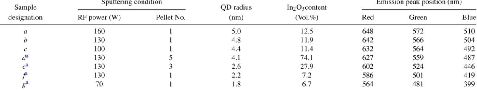
Figure2depicts the PL spectra and the de-convoluted profiles of In2O3QD-SiO2nanocomposite samples obtained by Gaussian curve
fitting method.25For the samples a-c prepared within the non-sintered
In2O3 pellets, the emission spectra locate mainly at the wavelength
range of 400 to 750 nm with a moderate difference in profile shape. On the contrary, dramatic differences in emission intensity and pro-file shape were observed in samples d-g prepared by using the sin-tered In2O3 pellets. Moreover, the samples with severe QD
over-lapping/coalescence, e.g., samples d and e, exhibit insignificant PL intensities in comparison with samples f and g containing uniformly dispersed, discrete In2O3QDs. In particular, emission intensities are
drastically enhanced for samples f and g, revealing the interfacial and quantized effects contributed by the embedment of sufficiently small In2O3QDs in such samples.
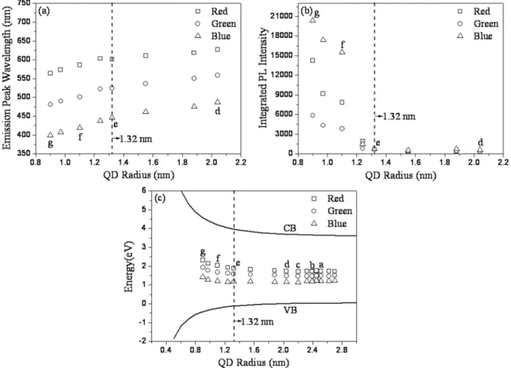
As illustrated by the curving fitting results of PL spectra shown in Fig.2, all spectra could be de-convoluted into red, green and blue emission bands. The corresponding emission peak positions summa-rized in TableIindicate, as the QD size decreases, all emissions shift toward the short wavelength side. As indicated by the plots of peak positions and integrated intensities of emission bands against the QD radius shown in Figs.3aand3b, the blueshift and emission efficiencies become pronounced when the QD radius is less than 1.32 nm. Such a phenomenon was ascribed to the quantum confinement effect since the strong confinement emerged when the QD radius is less than the Bohr radius. Notably, the Bohr radius deduced from the PL analysis is about equal to the low bound value of Bohr radii in a range of 1.3 to 11.4 nm reported by previous studies.11,20,21This is further validated
by the calibration of defect trap levels presented as follows.
Assume the PL properties of samples are correlated with the tran-sitions of electrons from conduction band edge (Ec) to the defect trap levels in In2O3QDs. The energetic position of the defect trap level in
an In2O3QD can thus be expressed as
Etr ap= Ec− Eemi ssi on (1)
) unless CC License in place (see abstract). ecsdl.org/site/terms_use
address. Redistribution subject to ECS terms of use (see 140.113.38.11
ECS Solid State Letters, 1 (2) R9-R12 (2012) R11
Figure 2. Curve fitting results for PL spectra for In2O3QD-SiO2nanocomposite samples a-g.
where Etrapis the energetic position of the defect trap level and Eemission is the photon energy of the emission band. The Ecand edge of the valence band (Ev) can be also expressed as functions of the QD radius in terms of the Brus’ model:26,27
Ec= Eg+ h2 8m∗er2 − 0.9e2 4πε0ε∞r (2) and Ev= h 2 8m∗hr2 −4πε0.9e2 0ε∞r (3) where Egfor the bulk In2O3is 3.75 eV, r is the QD radius, m∗eis the effective mass of electron (=0.35 mo), m∗h is the effective mass of hole (= 0.6 mo) andε∞is the high-frequency dielectric constant for
In2O3(=7).24By plugging the QD sizes and PL data listed in TableI
into Eqs.(1)–(3), one is able to plot the defect trap levels and their energetic positions in the bandgap of In2O3 against the QD radius
as depicted in Fig.3c. An obvious shift of trap levels occurs when QD radius is less than 1.32 nm, in agreement with the finding of PL properties. The Bohr radius of In2O3QDs was hence identified the as
1.32 nm.
Conclusions
In conclusion, the nanocomposite samples containing In2O3QDs
with sizes ranging from 1.8 to 5 nm embedded in SiO2 matrix were
prepared by utilizing the target-attachment sputtering method. TEM analysis revealed the In2O3 QDs are single crystalline with BCC
structure. The PL spectra of In2O3 QD-SiO2 nanocomposite layers
) unless CC License in place (see abstract). ecsdl.org/site/terms_use
address. Redistribution subject to ECS terms of use (see 140.113.38.11
R12 ECS Solid State Letters, 1 (2) R9-R12 (2012)
Figure 3. (a) Peak position and (b) integrated intensity of red, green and blue emissions deduced from the de-convoluted PL spectra of In2O3 QD-SiO2
nanocomposite samples as a function of QD radius. (c) The energetic positions of defect trap levels of In2O3QDs versus the QD radius calibrated in term of
the Brus’ model. The red, green and blue emissions correspond to the transitions either from Ecto a specific Etrapor from a specific Etrapto Evas defined in Eqs.(1)–(3). The letters a-b in above figures denoted the designation of samples prepared in this work.
were found to comprise of the red, green and blue emissions and the emission peaks shift toward the shorter wavelength side when the QD size is decreased. Moreover, the blueshift became pronounced when the QD radius was smaller than 1.32 nm, implying the occurrence of strong confinement effects in the samples containing QDs with radii less than such a value. The blueshift phenomenon was found in good agreement with the plot of integrated PL intensities for the three emissions and the calibration of defect trap levels against the QD radius, which allowed the identification of the Bohr radius of In2O3
QDs as 1.32 nm.
Acknowledgments
This work is supported by National Science Council (NSC), Tai-wan, R.O.C., under the contract No. NSC100-2221-E-009-054-MY2. Assistance of TEM analysis provided by Dr. Wei-Lin Wang and Dr. Li Chang at Department of Materials Science and Engineering, National Chiao Tung University, Taiwan, R.O.C., is also deeply acknowledged.
References
1. X. H. Zhang, S. J. Chua, A. M. Yong, S. Y. Chow, H. Y. Yang, S. P. Lau, and S. F. Yu,
Appl. Phys. Lett., 88, 221903 (2006).
2. B. Damilano, N. Grandjean, F. Semond, J. Massies, and M. Leroux,Appl. Phys. Lett., 75, 962 (1999).
3. J. Lee, V. C. Sundar, J. R. Heine, M. G. Bawendi, and K. F. Jensen,Adv. Mater., 12, 1102 (2000).
4. R. L. Weiher and R. P. Ley,J. Appl. Phys., 37, 299 (1966).
5. Z. B. Zhou, R. Q. Cui, Q. J. Pang, Y. D. Wang, F. Y. Meng, T. T. Sun, Z. M. Ding, and X. B. Yu,Appl. Surf. Sci., 172, 245 (2001).
6. Y. X. Liang, S. Q. Li, L. Nie, Y. G. Wang, and T. H. Wang,Appl. Phys. Lett., 88, 193119 (2006).
7. M. Curreli, C. Li, Y. H. Sun, B. Lei, M. A. Gundersen, M. E. Thompson, and C. W. Zhou,J. Am. Chem. Soc., 127, 6922 (2005).
8. T. Hibino, S. Tanimoto, S. Kakimoto, and M. Sanob,Electrochem. Solid-State Lett., 2, 651 (1999).
9. C. Y. Kuo, S. Y. Lu, and T. Y. Wei,J. Cryst. Growth, 285, 400 (2005).
10. B. Li, Y. Xie, M. Jing, G. Rong, Y. Tang, and G. Zhang,Langmuir, 22, 9380 (2006). 11. C. H. Liang, G. W. Meng, Y. Lei, F. Phillipp, and L. D. Zhang,Adv. Mater., 13, 1330
(2001).
12. X. C. Wu, J. M. Hong, Z. J. Han, and Y. R. Tao,Chem. Phys. Lett., 373, 28 (2003). 13. M. Mazzera, M. Zha, D. Calestani, A. Zappettini, L. Lazzarini, G. Salviati, and
L. Zanotti,Nanotechnology, 18, 355707 (2007).
14. Y. Shigesato and D. C. Paine,Thin Solid Films, 238, 44 (1994).
15. H. Kobayashi, T. Ishida, K. Nakamura, Y. Nakato, and H. Tsubomura,J. Appl. Phys., 72, 5288 (1992).
16. M. Higuchi, M. Sawada, and Y. Kuronuma,J. Electrochem. Soc., 140, 1773 (1993). 17. J. S. Cho, K. H. Yoon, and S. K. Koh,J. Appl. Phys., 89, 3223 (2001).
18. R. B. H. Tahar, T. Ban, Y. Ohya, and Y. Takahashi,J. Appl. Phys., 82, 865 (1997). 19. A. Murali, A. Barve, V. J. Leppert, S. H. Risbud, I. M. Kennedy, and H. W. H. Lee,
Nano Letters, 1, 287 (2001).
20. H. J. Zhou, W. P. Cai, and L. D. Zhang,Appl. Phys. Lett., 75, 495 (1999). 21. W. Yin, D. V. Esposito, S. Yang, C. Ni, J. G. Chen, G. Zhao, Z. Zhang, C. Hu, M. Cao,
and B. Wei,J. Phys. Chem. C, 114, 13234 (2010).
22. S. Das, S. Chakrabarti, and S. Chaudhuri,J. Phys. D: Appl. Phys., 4021 (2005). 23. M. G. Panthani, V. Akhavan, B. Goodfellow, J. P. Schmidtke, L. Dunn,
A. Dodabalapur, P. F. Barbara, and B. A. Korgel,J. AM. CHEM. SOC., 130, 16770 (2008).
24. Y. Y. Peng and T.-E. Hsieh,Appl. Phys. Lett., 89, 211909 (2006).
25. J. H. Noggle, Practical curve fitting and data analysis: software and self-instruction for scientists and engineers, Ellis Horwood, Hemel Hempstead (1993).
26. L. E. Brus,J. Phys. Chem., 90, 2555 (1986).
27. A. van Dijken, E. A. Meulenkamp, D. Vanmaekelbergh, and A. Meijerink,J. Lumin., 90, 123 (2000).
) unless CC License in place (see abstract). ecsdl.org/site/terms_use
address. Redistribution subject to ECS terms of use (see 140.113.38.11