IEEE TRANSACTIONS ON DEVICE AND MATERIALS RELIABILITY, VOL. 14, NO. 2, JUNE 2014 715
A Novel 3D Integration Scheme for Backside
Illuminated CMOS Image Sensor Devices
Cheng-Ta Ko, Zhi-Cheng Hsiao, Hsiang-Hung Chang, Dian-Rong Lyu, Chao-Kai Hsu, Huan-Chun Fu,
Chun-Hsien Chien, Wei-Chung Lo, and Kuan-Neng Chen, Senior Member, IEEE
Abstract—A novel backside-illuminated CMOS image sensor
(BSI-CIS) scheme and process are developed and demonstrated.
This innovative scheme can be realized without fusion oxide
bond-ing and through-silicon via (TSV) fabrication. This wafer-level
TSV-less BSI-CIS scheme includes transparent ultrathin silicon
(
∼ 3.6 μm) and uses several bonding technologies. The
character-ization and assessment results indicate that the integration scheme
possesses excellent electrical integrity and reliability. In addition,
good quality results of the image functional test demonstrate the
excellent performance of this scheme. This novel scheme also
provides a realizable low-cost solution for the next-generation CIS
and further 3-D novel BSI-CIS scheme.
Index Terms—CMOS image sensor, backside illuminated, 3D
integration.
I. I
NTRODUCTIONT
HREE-DIMENSIONAL integrated circuit (3D IC)
pro-vides a promising solution to extend beyond Moore’s Law
in the next generation semiconductor technology. In addition,
it could be extensively applied for the different products such
as CMOS imager sensor (CIS) module, MEMS, LED, memory
stacking, and logic/memory stacking. Among these CIS has
been led into mass production by using through-silicon via
(TSV) wafer-level package. There are two different schemes
for CIS. One is front side illuminated (FSI) [1], [2], and
the other is backside illuminated (BSI) [3]–[7] image sensor.
The traditional FSI-CIS has suffered the quantum efficiency
issue [8] as the pixel size down to less than 1.4 μm. In
FSI-CIS, the metal interconnects are formed above the sensing
area, which leads to a narrow optical path and makes worse
sensitivity (fill factor < 50%) as pixel size becomes smaller and
smaller. The quantity of the input light is only half compared
with BSI-CIS which makes the sensing area above the metal
interconnects.
Manuscript received January 2, 2014; accepted March 10, 2014. Date of publication March 17, 2014; date of current version June 3, 2014. This work was supported in part by the Ministry of Economic Affairs, Ministry of Education in Taiwan, under ATU Program and in part by the National Science Council through Grant NSC 102-2221-E-009-160.
C.-T. Ko is with the Department of Electronics Engineering, National Chiao Tung University, Hsinchu 300, Taiwan, and also with the Electronics and Optoelectronics Research Laboratories, Industrial Technology Research Insti-tute, Hsinchu 31040, Taiwan.
Z.-C. Hsiao, H.-H. Chang, C.-K. Hsu, H.-C. Fu, C.-H. Chien, and W.-C. Lo are with the Electronics and Optoelectronics Research Laboratories, Industrial Technology Research Institute, Hsinchu 31040, Taiwan.
D.-R. Lyu and K.-N. Chen are with Department of Electronics Engi-neering, National Chiao Tung University, Hsinchu 300, Taiwan (e-mail: [email protected]).
Color versions of one or more of the figures in this paper are available online at http://ieeexplore.ieee.org.
Digital Object Identifier 10.1109/TDMR.2014.2311887
For the BSI-CIS process, the CIS wafer is generally bonded
to a carrier wafer by oxide-oxide fusion bonding and followed
by a high temperature (> 300
◦C usually) annealing [9]–[11]. In
order to obtain a good bonding quality and strength,
chemical-mechanical polishing (CMP) is necessary to obtain a surface
roughness less than 1 nm. After bonding, the CIS wafer is
thinned down to few microns, and followed by color filter
formation and glass bonding for protection. Subsequently, the
carrier wafer is thinned and the TSVs are fabricated for power
and signal interconnection. However, the oxide fusion bonding
is an expensive and complex process inclusive of PECVD
oxide, CMP, surface clean, plasma activation, wafer bonding,
and post-bond annealing. In addition, the processes for TSV
fabrication are also very complex and expensive. In this paper,
we demonstrate a novel BSI-CIS structure and process, where
no carrier wafer required and the complex fusion bonding
and TSV fabrication processes can be skipped accordingly.
The electrical characteristics and reliability assessment of this
scheme are also investigated and discussed in the paper.
II. S
TRUCTURALD
ESIGN ANDC
OMPARISONIn BSI-CIS, as shown in Fig. 1(a), the CIS wafer is generally
attached to a carrier TSV wafer by oxide-oxide fusion bonding,
followed by a high temperature (> 300
◦C) annealing [4]–[6].
For good bonding quality and strength, chemical-mechanical
polishing (CMP) is necessary to obtain a surface roughness
less than 1 nm. After bonding, the CIS wafer is thinned down
to few microns, followed by color filter formation and glass
bonding for protection. Finally, carrier wafer thinning and TSV
fabrication are performed to complete process. However, this
scheme includes the oxide fusion bonding and TSV fabrication,
both are costly and complicated.
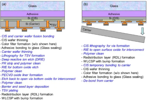
Compared to Fig. 1(a), Fig. 1(b) shows our novel BSI-CIS
scheme. With the wafer handling technology, the innovative
scheme can be realized without the complex fusion bonding
and TSV fabrication processes. As the process steps shown in
Fig. 1, where the italic type (blue color) presents the different
process required, this novel TSV-less scheme simplifies the
steps significantly, which can lead the fabrication cost reduced
greatly. The thermal budget and stress can be saved with
low temperature (< 200
◦C) adhesive bonding instead of high
temperature (> 300
◦C) annealing for oxide fusion bond. In
addition, without the carrier TSV wafer, the overall thickness
of this CIS module can be reduced significantly for future 3D
applications.
1530-4388 © 2014 IEEE. Personal use is permitted, but republication/redistribution requires IEEE permission. See http://www.ieee.org/publications_standards/publications/rights/index.html for more information.
716 IEEE TRANSACTIONS ON DEVICE AND MATERIALS RELIABILITY, VOL. 14, NO. 2, JUNE 2014
Fig. 1. Structural design and process comparison between (a) conventional and (b) our novel BSI-CIS scheme. The italic wording presents the different processes required in these two schemes, which indicates the novel BSI-CIS scheme simplifies process steps significantly.
Fig. 2. The schematic process flow of the novel TSV-less BSI-CIS structure, including the following steps: (a) CIS wafer with photodiode and multilayer metallization; (b) WLCSP with RDL and bump formation; (c) CIS temporary bonding to carrier; (d) CIS wafer thinning down to less than 5 μm; (e) color filter formation and glass sealing; and (f) carrier de-bond and soldering.
III. P
ROCESS ANDI
NTEGRATIOND
EMONSTRATIONFig. 2 shows the detailed schematic process flow of this
TSV-less BSI-CIS structure: (a) CIS wafer is prepared with
photodiode formation and multilayer metallization; (b) the
passivation is opened to reveal the metal pads, followed by
WLCSP with redistribution layer (RDL) and Ti/Cu
under-bump metallization (UBM) formation; (c) CIS wafer is then
temporarily bonded to a silicon carrier with adhesive material;
(d) CIS wafer is thinned down to less than 5 μm; (e) the
ultra-thinned CIS wafer is executed color filter formation, and then
permanently bonded to a 500 μm glass wafer for the sensing
area protection and handling carrier; (f) with the backside
glass wafer handling, the front side silicon carrier is de-bonded
followed by the solder bump formation on top of CIS wafer for
I/O fan out interconnect.
Critical process and integration steps are presented in Fig. 3.
Fig. 3(a) shows the fabricated CIS wafer with RDL and Cu pad
formation. The micro-bump is processed at the front side of the
wafer after sputtering. The wafer then is temporarily bonded
to a silicon carrier with HT-10.10, a thermal plastic material
from Brewer Science. Next, the CIS is thinned down to less than
5 μm by DISCO grinding and CMP system. It should be noted
that the total thickness variation (TTV) control after temporary
bonding is very important, as shown in Fig. 3(b). Fig. 3(c)
shows the ultra-thinned wafer without any chipping and cracks.
This CIS wafer is then permanently bonded to a 500-μm-thick
glass wafer for the sensing area protection and handling. After
edge cutting treatment, the silicon carrier is de-bonded by SUSS
DB12T de-bonder, and then the CIS surface is cleaned by SUSS
AR12 cleaner. Finally, 30-μm-diameter and 3-μm-thick Cu/Sn
micro-bumps are formed on the front side of the CIS based on
the pre-sputtered Ti/Cu UBM, as shown in Fig. 3(d). Fig. 3(e)
presents the completed 300 mm TSV-less BSI-CIS wafer with
well-developed process and integration. With ultra-thin silicon,
the final wafer is visible-light transparent as Fig. 3(f) presents.
Therefore, without oxide fusion bonding and TSV fabrication,
this scheme successfully provides a potential low cost solution
for BSI-CIS applications.
IV. E
LECTRICALC
HARACTERIZATION ANDR
ELIABILITYA
SSESSMENTIn this study, the packaged BSI-CIS module was
assem-bled onto a silicon interposer substrate by flip chip bonding
KO et al.: NOVEL INTEGRATION SCHEME FOR BSI CMOS IMAGE SENSOR DEVICES 717
Fig. 3. Process and integration demonstration of TSV-less BSI-CIS scheme, including the following steps: (a) CIS wafer with circuits and metallization; (b) WLCSP with RDL and Cu pad formation, and ready for temporary bonding; (c) CIS wafer thinning to < 5 μm without any chipping and cracks; (d) 30-μm-diameter Cu/Sn micro-bump formation on the front side of the CIS; (e) a completed TSV-less BSI-CIS wafer-level packaging; and (f) demonstra-tion of transparent BSI-CIS with ultra-thinned silicon.
technology. The silicon substrate was prepared with RDL,
elec-troless nickel, and immersion gold (ENIG) UBM formation.
Fig. 4(a) shows the assembled CIS/substrate bonding module.
Daisy chain feature and Kelvin structure were designed in the
scheme for electrical characterization and reliability
assess-ment. Fig. 4(b) shows the cross-sectional SEM image of the
ultra-thin silicon (
∼3.6 μm) BSI-CIS bonding with substrate
through the Cu/Sn micro-bump and ENIG UBM.
The characteristics and reliability of the bonding module
were analyzed. Agilent 4156C probe station with four-point
probes was adopted for electrical measurement. The bond chain
structure with a series of Cu RDL and Cu/Sn/ENIG micro-joint
interconnect was applied to investigate the electrical
charac-teristics of the integrated scheme, and the results are shown
in Fig. 5(a). The linear characteristic of total resistance versus
number of bond chain indicates excellent bonding integrity and
electrical performance. Fig. 5(b) shows the stable electrical
performance of four different structures under current stressing.
In addition, the characteristic of micro-joint interconnect was
investigated by Kelvin structure, and the results show the
con-tact resistance of single 30-μm-diameter Cu/Sn/ENIG bonded
interconnect is about 1.26 mΩ.
The bonded structure was fabricated for multiple cycles of
current stressing test, preconditioning test (JESD22-A113D,
Fig. 4. (a) Integrated CIS/Si substrate module. (b) SEM image of bonded structure.
Fig. 5. (a) Electrical characteristic of total resistance under different chain numbers. (b) Electrical performances of four different structure designs.
LV3), and temperature cycling test (TCT) (JESD22-A104B)
for reliability assessment. Fig. 6(a) and (b) shows the excellent
electrical stability even after 1000 cycles current stressing. The
test conditions of preconditioning and TCT are indicated in
Table I.
718 IEEE TRANSACTIONS ON DEVICE AND MATERIALS RELIABILITY, VOL. 14, NO. 2, JUNE 2014
Fig. 6. (a) Specific contact resistance results under multiple current stressing. (b) Daisy chain measurement results under multiple current stressing.
TABLE I
THETESTCONDITIONS OFPRECONDITIONING ANDTCT RELIABILITY
ASSESSMENT
As the results shown in Fig. 7(a), these structures can pass
1000 cycles of TCT test without apparent resistance variation.
The small specific contact resistance of single bonded
intercon-nect is even reduced from 3.94E-8 Ω-cm
2to 2.42E-8 Ω-cm
2after 1000 cycles of TCT as Fig. 7(b) presents. The reduction
may come from the improvement of bonded interface, such as
the grain growth and removal of defects [12]. These assessment
results indicate that the integration scheme possesses excellent
reliability and electrical stability, which is beneficial for the
further 3D integrated imager applications.
V. CMOS I
MAGES
ENSORF
UNCTIONALT
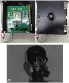
ESTThe integrated CIS module was verified with the image
func-tional test. Fig. 8(a) shows the developed system for the image
functional test, and Fig. 8(b) presents the image output result.
Herein the CIS device was fabricated with 0.18 μm generic
1P6M CMOS technology from TSMC, and packaged with our
novel TSV-less BSI-CIS WLP scheme. The pixel size is 3 μm
with three mega pixels (2048
× 1536) resolution. Because the
Fig. 7. (a) Resistance values before and after TCT. (b) Measurement results of specific contact resistance before and after TCT.
Fig. 8. (a) System development and set-up for the image functional test. (b) Image output result.
color filter formation was skipped, the image is black-white
color only. However, the image function is successfully verified
with good quality, which indicates the excellent performance
with this novel scheme and process integration. Based on these
results, this novel 3D-integration BSI-CIS scheme, including
analog-to-digital converter (ADC) and image signal processor
(ISP) integration with specific array design, can be fabricated
for a possible high resolution and frame rate (> 100 fps)
application.
KO et al.: NOVEL INTEGRATION SCHEME FOR BSI CMOS IMAGE SENSOR DEVICES 719
VI. C
ONCLUSIONIn this study, we successfully develop and demonstrate a
novel BSI-CIS structure and process flow based on 3D
integra-tion technologies. The innovative scheme can be realized
with-out the complex fusion bonding and TSV fabrication processes.
The characteristics and reliability of the scheme are
investi-gated, indicating excellent integration integrity and reliability.
In addition, the image function is successfully verified with
good quality, which indicates the excellent performance as well.
This scheme provides a realizable low cost solution for the next
generation CIS and further 3D integrated imager applications.
R
EFERENCES[1] D. Henry, F. Jacquet, M. Neyret, X. Baillin, T. Enot, V. Lapras, C. Brunet-Manquat, J. Charbonnier, B. Aventurier, and N. Sillon, “Through silicon vias technology for CMOS image sensors packaging,” in Proc. 58th Electron. Compon. Technol. Conf., May 2008, pp. 556–562. [2] M. Makoto and K. Mitsumasa, “3D-LSI technology for image sensor,”
J. Instrum., vol. 4, no. 3, p. P03009, Mar. 2009.
[3] J. A. Burns, B. F. Aull, C. K. Chen, C. L. Chen, C. L. Keast, J. M. Knecht, V. Suntharalingam, K. Warner, P. W. Wyatt, and D. R. W. Yost, “A wafer-scale 3-D circuit integration technology,” IEEE Trans. Electron Devices, vol. 53, no. 10, pp. 2507–2516, Oct. 2006.
[4] H. Rhodes, “The mass production of BSI CMOS image sensors,” in
Inter-national Image Sensors Workshop (IISW), Bergen, Norway, Jun. 2009.
[5] G. Meynants, J. Bogaerts, X. Wang, and G. Vanhorebeek, “Backside illuminated global shutter CMOS image sensors,” in Proc. Int. Image
Sensor Workshop, 2011, pp. R51–R54.
[6] X. Wang, B. Wolfs, J. Bogaerts, G. Meynants, T. Saito, and A. BenMoussa, “High dynamic range (HDR) back-side illuminated (BSI) CMOS image sensor for extreme UV detection,” Proc. SPIE, vol. 8298, pp. 82980B-1–82980B-8, Feb. 2012.
[7] P. Vu, B. Fowler, C. Liu, S. Mims, P. Bartkovjak, H. Do, W. Li, J. Appelbaum, and A. Lopez, “High dynamic range 4Mpixel CMOS image sensor for scientific applications,” Proc. SPIE-IS&T, vol. 8298, pp. 82980D-1–82980D-10, Feb. 2012.
[8] R. Fontaine, “Recent innovations in CMOS image sensors,” in Proc. IEEE
Adv. Semicond. Manuf. Conf., May 16–18, 2011, pp. 1–5.
[9] P. Coudrain, P. Batude, X. Gagnard, C. Leyris, S. Ricq, M. Vinet, A. Pouydebasque, N. Moussy, Y. Cazaux, B. Giffard, P. Magnan, and P. Ancey, “Setting up 3D sequential integration for back-illuminated CMOS image sensors with highly miniaturized pixels with low temper-ature fully depleted SOI transistors,” in Proc. IEEE Electron Devices
Meeting, Dec. 15–17, 2008, pp. 1–4.
[10] T. Matthias, G. Kreindl, V. Dragoi, M. Wimplinger, and P. Lindner, “CMOS image sensor wafer-level packaging,” in Proc. IEEE Electron.
Packag. Technol. High Density Packag., Aug. 8–11, 2011, pp. 1–6.
[11] K. Nam Hee, S. M. Hong, C. Yong-Won, L. Sun Jae, L. Han Gyul, K. Areum, K. Soo Won, K. Chang Hyun, and P. Sung Gyu, “Effect of planarity on the 3D integration in 3-D integrated CMOS image sensor,” in
Proc. 3D Syst. Integr. Conf., Jan. 31–Feb. 2, 2012, pp. 1–3.
[12] Y. J. Chang, C. T. Ko, and K. N. Chen, “Electrical and reliability in-vestigation of Cu TSVs with low-temperature Cu/Sn and BCB hybrid bond scheme,” IEEE Electron Device Lett., vol. 34, no. 1, pp. 102–104, Jan. 2013.
Cheng-Ta Ko received the B.S. and M.S. degrees in chemical engineering from National Taiwan Uni-versity, Taipei, Taiwan, in 2000 and 2002. He is currently working toward the Ph.D. degree in the De-partment of Electronics Engineering, National Chiao Tung University, Hsinchu, Taiwan. Since 2002, he has served in the Electronics and Optoelectronic Re-search Laboratories, Industrial Technology ReRe-search Institute, Hsinchu, where he is currently a Manager in the Packaging Technology Division. The focus of his research studies includes wafer-level packaging, system in package technology, flexible electronic packaging, and 3D IC tech-nologies.
Zhi-Cheng Hsiao received the M.S. degree in me-chanical engineer from National Taiwan Univer-sity of Science and Technology, Taipei, Taiwan, in 2002. Since 2003, he has served in the Electronics and Optoelectronic Research Laboratories, Industrial Technology Research Institute, Hsinchu, Taiwan. The focus of his research studies includes MEMS technology, micro bumping technology, wafer-level packaging, and 3D IC technologies.
Hsiang-Hung Chang received the Ph.D. degree from National Tsing Hua University, Hsinchu, Taiwan. Since 2002, he has served in the Electronics and Optoelectronic Research Laboratories, Industrial Technology Research Institute, Hsinchu, as a mem-ber of the Packaging Technology Division. The focus of his work is wafer bonding process, thin wafer han-dling process, process integration, and development of advanced package technology.
Dian-Rong Lyu received the B.S. degree in physics from National Sun Yat-sen University, Kaohsiung, Taiwan, in 2011. He is currently working toward the M.S. degree in the Institute of Electronics En-gineering, National Chiao Tung University, Hsinchu, Taiwan. The focus of his research studies includes wafer-level bonding, heterogeneous integration, and 3D IC technologies.
Chao-Kai Hsu received the B.S. degree in mechan-ical engineering from Chin-Yi University of Tech-nology, Taichung, Taiwan, in 1991. Since 2004, he has served in the Electronics and Optoelectronic Re-search Laboratories, Industrial Technology ReRe-search Institute, Hsinchu, Taiwan, where he is currently an Engineer in the Packaging Technology Division. The focus of his research studies includes wafer-level packaging, optical interconnects packaging, flexible electronic packaging, and 3D IC technologies.
Huan-Chun Fu received the M.S. degree in elec-trical engineering from Chang-Gung University, Taoyuan, Taiwan, in 2001. In 2000–2001, he served in the RD3 of Truelight Corporation. Since 2002, he has served in the Electronics and Optoelectronic Re-search Laboratories, Industrial Technology ReRe-search Institute, Hsinchu, Taiwan, where he is currently an Engineer in the Packaging Technology Division. The focus of his research studies includes wafer-level packaging, electrical and optical circuit board, and 3D IC technologies.
720 IEEE TRANSACTIONS ON DEVICE AND MATERIALS RELIABILITY, VOL. 14, NO. 2, JUNE 2014
Chun-Hsien Chien received the B.S. degree in chemical engineering from Fu Jen Catholic Uni-versity, New Taipei City, Taiwan, in 1995 and the M.S. degree in chemical engineering from National Tsing Hua University, Hsinchu, Taiwan, in 1997. In 1999, he served in United Microelectronics Corporation (UMC), Hsinchu, as Project Leader Engineer in advanced etching module. He is cur-rently a Project Manager in the Packaging Tech-nology Division, Electronics and Optoelectronic Research Laboratories, Industrial Technology Re-search Institute, Hsinchu. The focus of his reRe-search studies includes wafer-level packaging, embedded active device packaging, and 3D IC technologies.
Wei-Chung Lo received the Ph.D. degree in chem-istry from National Taiwan University, Taipei, Taiwan, in 1997. Since 1997, he has served in the Electronics and Optoelectronic Research Laboratories, Industrial Technology Research Institute, Hsinchu, Taiwan, where he is currently the Director of the Packaging Technology Division. He is currently the Executive Secretary of 3DIC consortium (Ad-STAC), Pro-gram Committee Chair of International Microsys-tems, Packaging, Assembly and Circuits Conference (IMPACT), and Chair of Advanced Microsystem and Packaging Alliance (AMPA), the largest package alliance in Taiwan.
Kuan-Neng Chen (M’05–SM’11) received the M.S. degree in materials science and engineering and the Ph.D. degree in electrical engineering and computer science from Massachusetts Institute of Technology, Cambridge, MA, USA. He is currently a Professor with the Department of Electronics Engineering, National Chiao Tung University, Hsinchu, Taiwan. Prior to the faculty position, he was a Research Staff Member with the IBM Thomas J. Watson Research Center, Yorktown Heights, NY, USA. His current research interests are three-dimensional integrated circuits, through-silicon via technology, wafer bonding technology, and het-erogeneous integration. Dr. Chen is a member of the Phi Tau Phi Scholastic Honor Society. He is currently the committee member of IEEE 3DIC, IEEE SSDM, and DPS. He was the recipient of two NCTU Distinguished Faculty Awards, two NCTU Outstanding Industry-Academia Cooperation Achievement Awards, Adventech Young Professor Award, EDMA Outstanding Youth Award, and five IBM Invention Plateau Invention Achievement Awards.