This content has been downloaded from IOPscience. Please scroll down to see the full text.
Download details:
IP Address: 140.113.38.11
This content was downloaded on 25/12/2014 at 02:55
Please note that terms and conditions apply.
Resistive switching characteristics of Pt/CeOx/TiN memory device
View the table of contents for this issue, or go to the journal homepage for more 2014 Jpn. J. Appl. Phys. 53 060303
(http://iopscience.iop.org/1347-4065/53/6/060303)
Resistive switching characteristics of Pt
/CeO
x/TiN memory device
Muhammad Ismail1,3, Ijaz Talib3, Chun-Yang Huang1, Chung-Jung Hung2, Tsung-Ling Tsai1,
Jheng-Hong Jieng1, Umesh Chand1, Chun-An Lin1, Ejaz Ahmed3, Anwar Manzoor Rana3,
Muhammad Younus Nadeem3, and Tseung-Yuen Tseng1*
1Department of Electronics Engineering and Institute of Electronics, National Chiao Tung University, Hsinchu 30010, Taiwan 2Department of Materials Science and Engineering, National Chiao Tung University, Hsinchu 30010, Taiwan
3Department of Physics, Bahauddin Zakariya University, Multan 60800, Pakistan E-mail: [email protected]
Received February 18, 2014; accepted March 24, 2014; published online May 15, 2014
The resistive switching characteristics of Pt/CeOx/TiN memory devices are investigated for potential applications in nonvolatile resistive random access memory (RRAM). The X-ray diffraction characteristics of the sputtered CeOxlayer indicate the formation of nanocrystalline single-phase CeO2 with a cubic fluorite structure. The existence of oxygen vacancies in the Pt/CeOx/TiN memory device was determined by X-ray photoelectron spectroscopic studies, while the presence of an interfacial layer between CeOxand the TiN bottom electrode was investigated by X-ray diffraction and high resolution transmission electron microscopy. The TiON layer formed at the TiN/CeOxinterface seems to play a key role in the resistive switching mechanism of the device. The present CeOx-based device shows excellent bipolar resistive switching characteristics, including a low operation current (100 µA), high ON/OFF resistance ratio (>105), and good retention/stress characteristics at both room temperature and 85 °C. ©2014 The Japan Society of Applied Physics
I
n recent years, resistive random access memory (RRAM) has attracted a great deal of attention from researchers. RRAM composed of a metal–insulator– metal (MIM) structure is being considered as a potential candidate to replace the flash memory in the near future. It demonstrates excellent characteristics including low power consumption, long data retention, high density integration, fast operational speed, high scalability, simple constituents, and low-cost nonvolatile memory applications.1) Many research groups have investigated RRAM using rare-earth materials2–4)and transition metal oxides.5)Rare-earth materi-als demonstrate very good resistive switching (RS) properties for nonvolatile memory. In addition, the transportation of oxygen vacancies/ions plays a key role in the resistive switching mechanism.6)Possessing a strong ability of oxygenion/vacancy migration and good RS behavior, cerium oxide (CeO2) thin films have gained a lot of interest for RRAM
applications.3,7) Moreover, CeO
2 films present multivalent
cations by exhibiting both +3 and +4 oxidation states and have high oxygen ion conductivity showing thir potential for valiancy change switching devices. In addition, the influence of the top/bottom electrode has been reported to enhance the window and stability for RS.8) Regarding the effect of the bottom electrode, it is shown that oxygen vacancies are generated due to the reaction between CeOx
and the TiN bottom layer.9) Consequently, an interfacial TiON layer is formed, which plays an important role in the RS behavior of the CeOx/TiN memory device by working
as an oxygen reservoir. The effect of Pt and Al as top electrodes on the RS behavior of CeO2 films has also been
studied.3,10) In fact, the set/reset voltage variability and
progressive degradation of the RS devices are still severe challenges. The RS phenomena and conduction mechanisms involved in CeO2-based devices are very important for
RRAM applications. However, there is lack of systematic studies in various configurations using different electrode materials and discussing the mechanisms of the RS properties of CeOxthinfilms.
In the present study, we report excellent bipolar resistive switching characteristics in the Pt/CeOx/TiN memory
de-vices with nonstoichiometric CeOx films. The influence of
TiN as a bottom electrode on the RS properties of CeOxfilms and the switching mechanisms are also investigated.
First, a 100-nm-thick layer of a TiN bottom electrode (BE) was deposited on a SiO2/Si substrate by an rf magnetron
sputter employing a TiN target with a sputtering power of 100 W. Then, CeO2 thinfilms (20–40 nm thick) were
depo-sited on that TiN/SiO2/Si substrate at room temperature by
the same magnetron sputter using a ceramic CeO2 target. A
base pressure of 1.2© 10¹6Torr was created in the chamber by a turbomolecular pump before deposition. The working pressure was maintained at 10 mTorr using a gas mixture of Ar and O2at a mixing ratio of6 : 18 with a total flow rate
of 20 sccm. The RF sputtering power of the system was set to 100 W. Finally, a 50-nm-thick Pt top electrode (TE) was deposited by dc magnetron sputtering on CeOx/TiN/SiO2/Si
using a metal shadow mask with a diameter of 150 µm. The morphology and crystal structure were examined by high-resolution transmission electron microscopy (HRTEM) and X-ray diffraction (XRD), respectively. X-ray photoemission spectroscopy (XPS) analysis was performed to identify the composition of the CeOx film in the device. The thickness of different layers were confirmed by HRTEM. The electrical characteristics of the device were measured using a semi-conductor parameter analyzer (Agilent B1500A) at room temperature. During electrical measurements, a bias voltage was applied to Pt TE keeping the TiN BE grounded.
The XRD pattern of the Pt/CeOx/TiN memory device
shown in Fig. 1(a) indicates the formation of a single-phase polycrystalline CeO2showing a cubicfluorite structure. From
the broadness and weak intensity of diffraction peaks, the poor crystalline structure can be inferred and defects such as oxygen vacancies may be anticipated in the film matrix. Moreover, few weak reflections corresponding to the TiON monoclinic structure are also observed as marked in Fig. 1(a). Figure 1(b) illustrates a cross-sectional TEM image of the Pt/CeOx/TiN/SiO2/Si RRAM device demonstrating
an apparent interface between CeOx and the TiN bottom
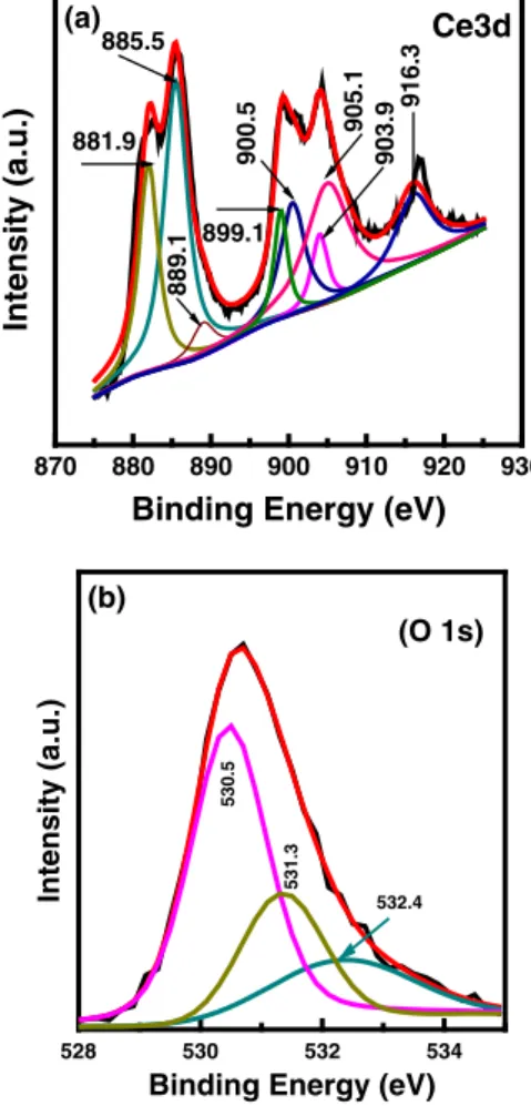
electrode. Regarding the chemical surface composition and the valence/oxidation state of various species, Fig. 2(a) displays the Ce 3d XPS spectrum of CeOxfilms along with
their corresponding deconvoluted plots. The XPS peaks http://dx.doi.org/10.7567/JJAP.53.060303
located at 881.9, 885.5, and 889.1 eV correspond to Ce 3d5/2, while peaks at 899.1, 900.5, 903.9, 905.1, and 916.3 eV are attributed to Ce 3d3/2. The XPS features at 885.5 and 903.9 eV are the characteristic peaks of Ce3+, and the peak at 916.3 eV corresponds to the initial electronic state of the Ce4+ ion.11,12) This implies that both Ce4+ and Ce3+ ions coexist
as Ce4+/Ce3+ pairs in the CeOx layer. The concentrations of Ce4+ and Ce3+ as obtained from the deconvoluted XPS spectra are 39.6 and 60.4%, respectively. A higher percentage of Ce3+ ions indicates the richness of oxygen vacancies.13) It is reported that Ce3+ ions distribute themselves around oxygen vacancies in CeO2and their presence would enhance
the local electronic conductivity of the oxide.14) Under an external bias, if the field of Ce3+ ions bridges the top and bottom electrodes, conductive paths would be formed to switch the device from high resistance state (HRS) to low resistance state (LRS). Figure 2(b) shows the O 1s XPS spec-trum of the Pt/CeOx/TiN device consisting of three peaks
at binding energies of 530.5, 531.3 and 532.4 eV, which can be attributed to lattice oxygen,15) oxygen vacancies,16)
and oxygen ions12) in CeO
2 respectively. Furthermore,
Holgado et al.17) have shown that the removal of oxygen
during sputtering may lead to the formation of Ce3+ ions, which causes the development of a new peak in the O 1s spectrum at a binding energy of 532.4 eV and they attributed the peak to oxygen ions at the surface (and grain boundaries) of the film.
Figure 3(a) depicts the current vs bias voltage sweep char-acteristics demonstrated for CeOx films with varying thick-ness in the range of 20–40 nm indicating the negative SET and positive RESET typical for bipolar RS memory. Initially, by sweeping the bias voltage from 0 to ¹3 V, a sudden increase in the current of all three devices is observed with a current compliance of 1 mA switching them to a LRS. A notable point is the magnitude of the negative bias voltage needed to switch the device from HRS to LRS, which increases with a rise in thickness of the sandwiched CeOx
film. Such a dependence of Vset upon the thickness of the
CeOx films signifies that the SET process is a field-induced
phenomenon. However, the bias voltage needed for the subsequent RESET process is not evidently affected by the thickness of the CeOxfilm. Consequently, the electric power
needed for the rupture of conductive filaments is the same for all three devices. Typical forming free bipolar resistive switching characteristics of a Pt/CeOx/TiN RRAM memory
device are displayed in Fig. 3(b). Figure 3(b) that the fresh device is originally in the high resistance state and the negative SET voltage of the 1st sweep is almost the same as those of the 100th and 200th sweeps in contrast to the devices which need a large (forming) voltage for their first SET process. As far as power consumption in the device prepara-tion for repeatable resistive switching is concerned, such forming free resistive switching behavior is very promising from an RRAM application point of view.2,18)
30 40 50 60 70 80 TiN JCPDS # 761834 T iN (222) T iN (1 1 1 ) TiON JCPDS # 440951 Pt (1 1 1 ) Pt (220) Si (31 1) Si (220) SiO 2 (602) SiO 2 (333) CeO 2 (222) CeO 2 (200) CeO 2 (1 1 1 ) T iON (304) T iON (204) T iON(013) T iON (01 1) T iON (302) Intensity (a.u) 2θ (Degree) CeO2 JCPDS # 652975 (a)
Fig. 1. (a) XRD pattern of Pt/CeO2/TiN/SiO2/Si structure. (b) HRTEM
cross-sectional image of Pt/CeO2/TiN/SiO2/Si device.
870 880 890 900 910 920 930
Intensity (a.u.)
Binding Energy (eV) 885.5 881.9 889.1 899.1 900.5 905.1 903.9 916.3 Ce3d (a) 528 530 532 534 Intensity (a.u.)
Binding Energy (eV)
530.5
531.3
532.4
(b)
(O 1s)
Fig. 2. (Color online) XPS core level spectra of CeO2film (a) Ce 3d level
and (b) O 1s level.
Jpn. J. Appl. Phys. 53, 060303 (2014) M. Ismail et al.
To further evaluate the memory performance of the Pt/CeOx/TiN device, an endurance test is conducted at room
temperature and 85 °C, as shown in Fig. 4. The resistances were determined at afixed voltage of 0.3 V, while the set and reset operations were performed at negative and positive voltage polarities, respectively. The HRS resistance measured at 85 °C was lower than that at room temperature. The high resistance can be described as exhibiting a typical semi-conductor-like behavior,19) with the resistance decreasing by approximately 2 orders of magnitude upon increasing the temperature. However, the LRS resistance at 85 °C was slightly lower than that at RT, indicating once again the semiconducting behavior. The resistance ratio of HRS to LRS lies approximately in the range of 103–105 during the first
200 cycles. After 200 switching cycles, it can be seen that the device still has an acceptable memory window, demonstrat-ing its good repetitive switchdemonstrat-ing capability. On compardemonstrat-ing the results with a work9)on a similar Pt/CeO
x/TiN memory
device, it can be concluded that our device exhibits a larger memory window for read/write operations with low power consumption and a much better repetitive switching capa-bility. This may be attributed to the different conditions of the oxidefilm in the ReRAM device.
Figure 5(a) shows the retention performance of both HRS and LRS for the Pt/CeOx/TiN device. It is evident that
the device retains its ON/OFF state for more than 104s
without any apparent degradation at both room temperature and 85 °C. As shown in Fig. 5(b), the two resistance states are stable over 104s under a stress voltage of 0.3 V, without
any observable degradation at both room temperature and 85 °C, demonstrating excellent nondestructive readout capa-bility. Such superior data retention characteristics of the Pt/CeOx/TiN device reveal its potential for future nanoscale
nonvolatile memory applications.
0 50 100 150 200 10-9 10-8 10-7 10-6 10-5 10-4 10-3 10-2 LRS @ RT HRS @ RT LRS @ 85 °C HRS @ 85 °C
Current (A)
Number of Cycles (#)
Fig. 4. (Color online) Endurance characteristics of Pt/CeOx/TiN device
measured at RT and 85 °C. -3 -2 -1 0 1 2 3 10-10 10-9 10-8 10-7 10-6 10-5 10-4 10-3 10-2 3 4 Current (A) Voltage (V) 20nm 30nm 40nm (a) 1 2 Set Reset -3 -2 -1 0 1 2 3 10-9 10-8 10-7 10-6 10-5 10-4 10-3 10-2 Current (A) Voltage (V) 1st sweep 100th sweep 200th sweep (b) 1 2 3 4
Fig. 3. (Color online) (a) Current–voltage (I–V) characteristics as a function of CeO2film thickness that varies from 20 to 40 nm in Pt/CeOx/TiN
RRAM memory devices. (b) DC I–V cycling characteristics studied at Vread
of 0.3 V over 200 sweeps for 30-nm-thick CeO2memory device.
100 101 102 103 104 10-10 10-9 10-8 10-7 10-6 10-5 10-4 10-3 10-2 HRS LRS @ RT HRS LRS @ 85°C Current (A) Retention Time (s) (a) 100 101 102 103 104 10-10 10-9 10-8 10-7 10-6 10-5 10-4 10-3 10-2 Current (A) Stress Time (s) HRS LRS @ RT HRS LRS @ 85°C (b)
Fig. 5. (Color online) (a) Retention characteristics of HRS and LHS of Pt/CeOx/TiN device under a continuous reading voltage of 0.3 V. (b)
Non-destructive readout properties of both ON- and OFF-states at RT and 85 °C.
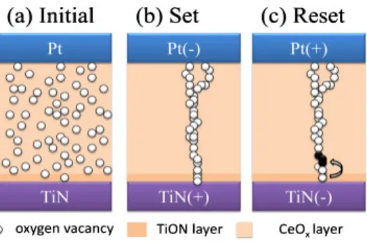
Figure 6 presents a schematic description about of the resistive switching mechanism of the device. In the pristine state, a large number of oxygen vacancies exist in the CeOx layer (Fig. 2). However, as these oxygen vacancies are randomly distributed and are not yet arranged to form con-ductivefilaments, the device is initially in HRS, as shown in Fig. 6(a). During the SET transition, when a negative bias voltage is applied to Pt TE, oxygen ions migrate from the CeOx layer to the bottom electrode and oxygen vacancies drift under the appliedfield to form the conductive filaments, and thus switch the device into LRS, as shown in Fig. 6(b). It is notable that the filamentary path starts to develop from the oxygen-deficient interfacial TiON layer near the BE. This interfacial TiON layer is formed due to the oxygen gettering property of TiN (which can take oxygen from the CeOxlayer
to form a partially oxidized TiON layer9)). The enhanced oxygen mobility facilitates the reduction of Ce4+cations, and creates more Ce3+and oxygen vacancies (Fig. 2). In contrast, the positive bias applied to the Pt top electrode attracts the oxygen ions from the TiON layer to drift back to the CeOx film thereby oxidizing the vacancies, hence rupturing the formed conductive path and resulting in a transition from LRS to HRS, as shown in Fig. 6(c). In this case, the TiON layer might be the source of mobile oxygen. The TiN BE thus works as an oxygen ion reservoir, which causes the migration of oxygen ions under an external bias hence contributing significantly to the resistance change.8,20,21)
Bipolar RS characteristics were successfully demonstrated in a Pt/CeOx/TiN device. The XRD pattern of a
magnetron-sputtered CeOx layer indicated the formation of a
single-phase CeO2 with a cubic polycrystalline fluorite structure.
The presence of oxygen vacancies was determined by XPS spectra while the presence of an interfacial layer between
CeO2 and TiN was detected from the HRTEM image. The
set voltage dependence on the thickness of the CeOxlayer
has indicated that the switching process is an electric-field-induced phenomenon. The TiN/CeOxinterface plays a key
role in controlling the oxygen vacancy defects, which in turn control the formation/rupture of conducting filaments composed of oxygen vacancies. The device exhibited a good cycling endurance with a large memory window (ratio of HRS/LRS about 105) and an acceptable retention/stress
test for 104s. The cycling endurance and data retention
capability of the device were found to be satisfactory at 85 °C.
Acknowledgements The authors acknowledge thefinancial support by the Higher Education Commission (HEC), Islamabad, Pakistan under the International Research Support Initiative Program (IRSIP). This work was also supported by the National Science Council, Taiwan, under project NSC NSC 99-2221-E009-166-MY3.
1) T. Y. Tseng and S. M. Sze, Nonvolatile Memories: Materials, Devices and Applications (American Scientific Publishers, Stevenson Ranch, CA, 2012) Vol. 2, Chaps. 5–14.
2) D. Panda and T. Y. Tseng,Thin Solid Films531, 1 (2013).
3) C.-Y. Lin, D.-Y. Lee, S.-Y. Wang, C.-C. Lin, and T.-Y. Tseng,Surf. Coatings Technol.203, 480 (2008).
4) K. C. Liu, W. H. Tzeng, K. M. Chang, Y. C. Chan, C. C. Kuo, and C. W. Cheng,Microelectron. Reliab.50, 670 (2010).
5) T. M. Pan and C. H. Lu,Appl. Phys. Lett.99, 113509 (2011).
6) S.-Y. Wang and T.-Y. Tseng,J. Adv. Dielectr.1, 141 (2011).
7) X. Cao, X. Li, X. Gao, W. Yu, X. Liu, Y. Zhang, L. Chen, and X. Cheng,
J. Appl. Phys.106, 073723 (2009).
8) C. Y. Lin, C. Y. Wu, T. C. Lee, F. L. Yang, C. Hu, and T. Y. Tseng,IEEE Electron Device Lett.28, 366 (2007).
9) Q. Zhou and J. Zhai,Integrated Ferroelectr.140, 16 (2012).
10) X. Sun, B. Sun, L. Liu, N. Xu, X. Liu, R. Han, J. Kang, G. Xiong, and T. P. Ma,IEEE Electron Device Lett.30, 334 (2009).
11) E. Bêche, P. Charvin, D. Perarnau, S. Abanades, and G. Flamant,Surf. Interface Anal.40, 264 (2008).
12) M. Ismail, C. Y. Huang, D. Panda, C. J. Hung, T. L. Tasi, J. H. Jeing, C. A. Lin, U. Chand, A. M. Rana, E. Ahmed, I. Talib, M. Y. Nadeem, and T. Y. Tseng,Nanoscale Res. Lett.9, 45 (2014).
13) F. Meng, C. Zhang, Q. Bo, and Q. Zhang,Mater. Lett.99, 5 (2013).
14) S. Deshpande, S. Patil, S. Kuchibhatla, and S. Seal,Appl. Phys. Lett.87, 133113 (2005).
15) R. Yu, L. Yan, P. Zheng, J. Chen, and X. R. Xing,J. Phys. Chem. C112, 19896 (2008).
16) D. Gao, G. Yang, L. Li, J. Zhang, J. Zhang, and D. Xue,J. Phys. Chem. C 114, 18347 (2010).
17) J. P. Holgado, G. Munuera, J. P. Espinós, and A. R. González-Elipe,Appl. Surf. Sci.158, 164 (2000).
18) C. Chen, Y. C. Yang, F. Zeng, and F. Pan,Appl. Phys. Lett.97, 083502 (2010).
19) J. L. Her, T. M. Pan, and C. H. Lu,Thin Solid Films520, 5706 (2012).
20) J. Kim, K. Lee, Y. Kim, H. Na, D.-H. Ko, H. Sohn, and S. Lee,Mater. Chem. Phys.142, 608 (2013).
21) M. Fujimoto, H. Koyama, M. Konagai, Y. Hosoi, K. Ishihara, S. Ohnishi, and N. Awaya,Appl. Phys. Lett.89, 223509 (2006).
Fig. 6. (Color online) Schematic diagram of resistive memory switching mechanism in Pt/CeOx/TiN memory device. (a) Initial state, (b) set to LRS and (c) reset back to HRS. Black circles indicate the rupture area of the device during the reset process.
Jpn. J. Appl. Phys. 53, 060303 (2014) M. Ismail et al.