This content has been downloaded from IOPscience. Please scroll down to see the full text.
Download details:
IP Address: 140.113.38.11
This content was downloaded on 26/04/2014 at 11:03
Please note that terms and conditions apply.
Comparison of the electronic structures of AlN nanotips grown on p- and n-type Si substrates
View the table of contents for this issue, or go to the journal homepage for more 2005 J. Phys.: Condens. Matter 17 7523
(http://iopscience.iop.org/0953-8984/17/48/006)
J. Phys.: Condens. Matter 17 (2005) 7523–7530 doi:10.1088/0953-8984/17/48/006
Comparison of the electronic structures of AlN
nanotips grown on p- and n-type Si substrates
J W Chiou1, H M Tsai1, C W Pao1, C L Dong1, C L Chang1, F Z Chien1, W F Pong1,8, M-H Tsai2, S C Shi3, C F Chen3, L C Chen4, K H Chen5, I-H Hong6,9, C-H Chen6, H-J Lin6and J H Guo7
1Department of Physics, Tamkang University, Tamsui, Taiwan 251, Republic of China 2Department of Physics, National Sun Yat-Sen University, Kaohsiung, Taiwan 804,
Republic of China
3Department of Materials Science and Engineering, National Chiao Tung University, Hsinchu,
Taiwan 300, Republic of China
4Centre for Condensed Mater Sciences, National Taiwan University, Taipei, Taiwan 106,
Republic of China
5Institute of Atomic and Molecular Science, Academia Sinica, Taipei, Taiwan 106,
Republic of China
6National Synchrotron Radiation Research Center, Hsinchu, Taiwan 300, Republic of China 7Advanced Light Source, Lawrence Berkeley National Laboratory, Berkeley, CA 94720-8226,
USA E-mail:[email protected] Received 5 September 2005 Published 11 November 2005 Online atstacks.iop.org/JPhysCM/17/7523 Abstract
Al and N K-edge x-ray absorption near-edge structure (XANES), scanning photoelectron microscopy (SPEM) and x-ray emission measurements were performed on AlN nanotips grown on p- and n-type Si substrates (p-AlN and n-AlN). Features and intensities in the Al and N K-edge XANES spectra of these AlN nanotips overall are similar. In contrast, the intensities of the valence-band SPEM spectra of p-AlN are apparently larger than those of n-AlN, which indicates that the valence-band density of states of p-AlN exceeds that of n-AlN. This result may be related to the observed enhancement of field-emission intensity of AlN nanotips grown on the p-type Si substrate.
1. Introduction
Aluminium nitride (AlN), a group-III nitride wide-band-gap semiconductor, is an important material for optoelectronic applications [1]. Recently, one-dimensional (1D) nanostructures of AlN have been of particular interest because they have a low turn-on field, high current
8 Author to whom any correspondence should be addressed.
9 Permanent address: Department of Applied Physics, National Chiayi University, Chiayi 600, Taiwan.
7524 J W Chiou et al
density and a very small, even negative, electron affinity [2–4]. Electron field emission involves tunnelling of electrons from the substrate into the semiconductor materials, the transport of carriers through the materials and their emission from the surface into vacuum [5]. Accordingly, electrons injected through substrate–emitter and the emitter–vacuum interfaces strongly influence the characteristics of electron emission [6]. The properties of the emitter– vacuum interface has been extensively studied. In contrast, the substrate–emitter interface has been rarely examined. Recently, Chang et al [7] and Shi et al [8] found that wide-band-gap SiCN and AlN 1D nanomaterials had larger field-emission intensities when they were grown on the p-type Si substrate than on the n-type substrate. They explained that the direction of band bending at the p-type substrate–emitter interface-assisted field emission. Thus, the knowledge of the dependence of the conduction band, valence band and band gap of these 1D nanomaterials grown on p- and n-type semiconductor substrates is crucial in understanding the basic physics relevant to nanotechnological applications of these materials. In particular, electron-field emission from 1D nanostructured emitters concerns electron tunnelling from conduction-band, valence-band and/or surface states [9]. For this purpose, x-ray absorption near-edge structure (XANES), scanning photoelectron microscopy (SPEM) and x-ray emission spectroscopy (XES) measurements were performed to obtain the details of the electronic structures of 1D AlN nanotips grown on p- and n-type Si substrates.
2. Experiment
Al and N K-edge XANES were measured in the fluorescence mode using Dragon and high-energy spherical grating monochromator beamlines. SPEM images and spectra were acquired using the U5-undulator beamline at the National Synchrotron Radiation Research Center (NSRRC), Hsinchu, Taiwan. XES and corresponding XANES measurements of the N 2p states were performed at the Advanced Light Source, Lawrence Berkeley National Laboratory, beamline-7.0.1, which has a spherical grating monochromator. The quasi-aligned AlN nanotips were synthesized by a thermal chemical vapour deposition process using p- and n-type Si substrates, which were doped with boron and phosphorus, respectively. AlN nanotips grown on p- and n-type Si substrates are denoted as p-AlN and n-AlN nanotips, respectively. The details of the preparation of p- and n-AlN nanotips have been reported elsewhere [8].
3. Results and discussion
Figure1presents x-ray diffraction measurements of AlN nanotips and the reference thin film sample. The prominent characteristic (100), (002) and (101) peaks in figure1 reveal that quasi-aligned AlN nanotips are polycrystalline and have a hexagonal (wurtzite) structure. Figures1(a)–(c) display typical top-view and cross-sectional SEM images of nanotips. The AlN nanotips have average diameters of∼10 nm at the apex and ∼100 nm at the bottom, and lengths of∼1500 nm. They exhibit very similar morphologies. Figure1(d) shows field-emission current densities, J , of p- and n-AlN nanotips as a function of the applied field obtained by Shi et al [8]. J for p-AlN nanotips rises rapidly when the applied field exceeds a threshold of about 5 Vµm−1. In comparison, J for n-AlN nanotips remains small. At an applied field of approximately 9 Vµm−1, J for p-AlN nanotips is four orders of magnitude larger than that for n-AlN nanotips. The field emission of nanostructured SiCN exhibited a similar property [7].
Figure2and lower inset present the XANES spectra of AlN nanotips and the reference thin film at the Al and N K-edge, respectively. The upper inset in figure2shows an incident
30 35 40 45 50 0 2 4 6 8 10 1E-10 1E-8 1E-6 1E-4 0.01 (200) n-AlN (101) (100) (002) p-AlN Thin film In te nsity (a rb. units) 2θ J (A /c m 2) Applied Field (V/µm) p -AlN n-AlN (a) (b) (c) (d)
Figure 1. XRD measurements of quasi-aligned AlN nanotips and the reference thin film. The insets
(a)–(c) display representative SEM images of the top view of p- and n-AlN nanotips and the cross-sectional view of p-AlN nanotips, respectively. The inset (d) plots field-emission characteristic curves of p- and n-AlN nanotips.
angle ofθ = 37◦ relative to the normal of the substrate. Features A1 to D1 (A2to D2) are
associated with the four features of the calculated Al (N) p-derived partial density of states (DOS) [10,11]. These features agree well with theσ bond (bi-layer bond) and the π bond (c-axis bond) XANES spectra of AlN film and bulk samples obtained previously [12–14]. The variation in the general lineshapes of the Al and N K-edge XANES spectra of AlN nanotips and the reference thin film with respect to the photon energy are similar to those observed previously in the Ga and N K-edge XANES spectra of GaN nanowires and thin-film sample [15] due to the same crystal structure and similar c/a ratio, where a and c are the wurtzite lattice constants. The general lineshapes in the Al and N K-edge XANES spectra of AlN nanotips and the thin film overall have similar features and intensities. Only the intensity of feature B1in the Al
K-edge XANES spectrum of n-AlN nanotips is noticeably smaller than those in the spectra of p-AlN nanotips and the thin film.
7526 J W Chiou et al 1560 1575 1590 1605 0 3 6 395 400 405 410 0 1 D1 C1 B1 A1 Al K-edge
Normalized Absorption (arb.units)
Photon Energy (eV)
p-AlN n-AlN Thin film D2 C2 B2 A2 N K-edge
Figure 2. Al and N (lower inset) K-edge XANES spectra of AlN nanotips and the reference thin
film. The upper inset shows the incident angleθ relative to the normal of the substrate.
Figure3displays spatially resolved valence-band photoemission spectra of AlN nanotips and the reference film. The Al 2p SPEM images (upper insets) show the cross-sectional view of AlN nanotips and the top view of the reference film. The lower inset in figure 3 also presents the valence-band photoemission spectra from the tip region of AlN nanotips. The bright areas in the SPEM images correspond to AlN nanotips with a maximum Al 2p intensity. The spectra displayed in figure3are total photoelectron yields from three selected positions in the side regions of p-AlN marked by p(s1), p(s2) and p(s3) and of n-AlN marked by n(s1), n(s2) and n(s3), and in the surface region of the reference thin film marked by f(1), f (2) and
f(3) as shown in the upper inset. The summation over three different positions is to avoid
deviations due to inhomogeneity in the samples. The zero energy refers to the Fermi level,
Ef, which is the threshold of the emission spectra. The spectra have broad features and are
dominated by N 2p–Al 2sp hybridized states [13,16]. The figure reveals that the intensities of the valence-band spectra in the sidewall regions in n-AlN nanotips are clearly smaller than
15 10 5 0 15 10 5 0 = Ef hν= 390 eV Valence Band Intensit y (a rb. units )
Binding Energy (eV) p-AlN
n-AlN Thin film
Tip region
= Ef
Figure 3. Valence-band photoemission spectra of the SPEM yields from the side regions of p- and
n-AlN and the reference thin film. These yields have been summed over three different positions, namely p(s1), p(s2) and p(s3) in p-AlN, n(s1), n(s2) and n(s3) in n-AlN, and f(1), f(2) and f(3) in the thin film, as shown in the upper inset, which present the Al 2p SPEM cross-sectional images of quasi-aligned AlN nanotips and the top view of the reference thin film, respectively. The lower inset presents the valence-band photoemission spectra summed over three selected tip regions p(t1), p(t2) and p(t3) in p-AlN and n(t1), n(t2) and n(t3) in n-AlN shown in the upper inset.
those in p-AlN nanotips and the thin film. The lower inset in figure3displays the sum of valence-band spectra contributed from p(t1)-p(t3) and n(t1)-n(t3) positions in the tip regions of p- and n-AlN nanotips, respectively, which shows that p-AlN nanotips have a larger SPEM intensity than n-AlN nanotips similar to those of sidewall regions.
As stated previously, Chang et al [7] and Shi et al [8] proposed a substrate–nanomaterial heterojunction model to explain why the electron transport across the substrate–emitter
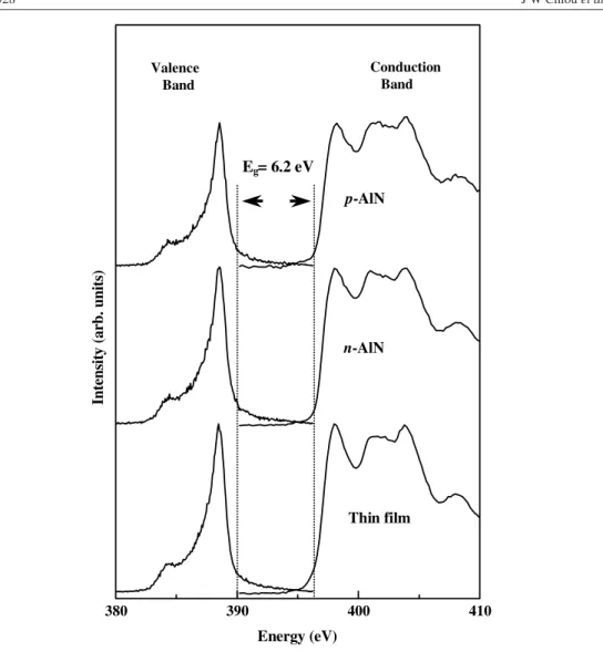
7528 J W Chiou et al 380 390 400 410 Eg= 6.2 eV Conduction Band Valence Band Thin film n-AlN p-AlN Intensit y (ar b. units) Energy (eV)
Figure 4. XES and corresponding XANES spectra of the N 2p states of AlN nanotips and the
reference thin film.
interface yields superior electrofield emission for the p-type Si substrate than for the n-type Si substrate for wide-band-gap SiCN nanomaterials and AlN nanotips. According to this model, Ef of the p-type Si substrate is slightly lower than that of the wide-band-gap 1D
nanostructured SiCN/AlN, which causes holes to flow from p-type Si to SiCN/AlN to align
Ef (i.e. the chemical potential) on both sides. The resultant band bending at the p-type Si–
SiCN/AlN interface gives rise to a ‘well’, which assists electron flow across this interface and leads to a more effective electron tunnelling into SiCN/AlN under an applied field. In contrast, a ‘barrier’ is formed at the n-type Si–SiCN/AlN interface, which hinders motion of electrons from Si to SiCN/AlN. Consequently, the nanostructured SiCN/AlN grown on the p-type Si substrate has a higher electron-emission current than that grown on the n-type Si substrate. The Al and N K-edge XANES spectra of AlN nanotips exhibit similar features and intensities, suggesting that the DOSs of the conduction band of both p- and n-AlN nanotips are similar. However, the intensities of valence-band SPEM spectra of p-AlN apparently exceed those of
n-AlN, which suggests that the valence-band DOS of p-AlN is larger than that of n-AlN, although the measurements were performed in the absence of an applied field. This result indicates that the intensity of field-emitted electrons is strongly correlated with the valence-band DOS of AlN nanotips.
Figure4presents XES and corresponding XANES spectra of N 2p states of AlN nanotips and the reference AlN thin film. The N K emission spectra reflect N 2p occupied (valence-band) states and N K-edge XANES spectra reflect N 2p unoccupied (conduction-(valence-band) states of AlN nanotips and the reference film. These spectra are consistent with the results of first-principles calculations [10,11] and the spectra of the AlN film obtained previously [12]. A well-defined band gap(Eg) between the valence-band maximum (VBM) and the
conduction-band minimum (CBM), marked by dotted lines, is observed, as shown in figure4. The emission and absorption spectra clearly indicate that the Egof 6.2 eV for AlN nanotips is the same as
that of the reference thin film, which also agrees with earlier studies [12,17]. The positions of the VBM and CBM are also found to be the same for p- and n-AlN nanotips and the reference thin film, which illustrates that the VBM, CBM and Egof AlN nanotips are not affected by
either p- and n-type Si substrates when no field is applied.
4. Conclusion
In summary, Al and N K-edge XANES measurements for AlN nanotips grown on p- and n-type Si substrates exhibit similar features and intensities, suggesting that the DOSs of the conduction-band of both p- and n-AlN nanotips are similar. In contrast, the intensities of the valence-band SPEM spectra of p-AlN are apparently larger than those of n-AlN, which indicates that the valence-band DOS of p-AlN exceeds that of n-AlN. This result correlates with the observed enhancement of field-emission intensity of AlN nanotips grown on the p-type Si substrate.
Acknowledgments
One of the authors (WFP) would like to thank the National Science Council (NSC) of the Republic of China for financially supporting this research under Contract No. NSC 93-2112-M032-018. The work at ALS, Lawrence Berkeley National Laboratory, was supported by the US Department of Energy, under contract No. DE-AC03-76SF00098.
References
[1] Sakai H, Koide T, Suzuki H, Yamaguchi M, Yamasaki S, Koike M, Amano H and Akasaki I 1995 Japan. J.
Appl. Phys.34 L1429
[2] Bonard J M, Kind H, St¨ockli T and Nilsson L O 2001 Solid-State Electron.45 893
[3] Wu Q, Hu Z, Wang X, Lu Y, Huo K, Deng S, Xu N, Shen B, Zhang R and Chen Y 2003 J. Mater. Chem.13 2024 [4] Wu C I, Kahn A, Hellman E S and Buchanan D N E 1998 Appl. Phys. Lett.73 1346
Wu C I and Kahn A 2000 Appl. Surf. Sci.162/163 250 [5] Baumann P K and Nemanich R J 1998 J. Appl. Phys.83 2072
[6] Show Y, Matsuoka F, Hayashi M, Ito H, Iwase M and Izumi T 1998 J. Appl. Phys.84 6351
[7] Chang C S, Chattopadhyay S, Chen L C, Chen K H, Chen C W, Chen Y F, Collazo R and Sitar Z 2003 Phys.
Rev. B68 125322
[8] Shi S C, Chen C F, Chattopadhyay S, Chen K H and Chen L C 2005 unpublished
[9] Modinos A 1984 Field, Thermonic, and Secondary Electron Emission Spectroscopy (New York: Plenum) [10] Tang Y-H and Tsai M-H 2005 J. Appl. Phys.97 103702
7530 J W Chiou et al [12] Duda L-C, Stagarescu C B, Downes J, Smith K E, Korakakis D, Moustakas T D, Guo J H and Nordgren J 1998
Phys. Rev. B58 1928
[13] Lawniczak-Jablonska K, Suski T, Gorczyca I, Christensen N E, Attenkofer K E, Perera R C C, Gullikson E M, Underwood J H, Ederer D L and Weber Z L 2000 Phys. Rev. B61 16623
[14] Mizoguchi T, Tanaka I, Yoshioka S, Kunisu M, Yamamoto T and Ching W Y 2004 Phys. Rev. B70 045103 [15] Chiou J W, Jan J C, Tsai H M, Pong W F, Tsai M-H, Hong I-H, Klauser R, Lee J F, Hsu C W, Lin H M,
Chen C C, Shen C H, Chen L C and Chen K H 2003 Appl. Phys. Lett.82 3949
[16] Martin G, Strite S, Botchkarev A, Agarwal A, Rockett A, Morkoc H, Lambrecht W R L and Segall B 1994 Appl.
Phys. Lett.65 610