Diamond nucleation on Cu by using MPCVD
with a biasing pretreatment
Kun-Lin Chuang, Li Chang
∗, Chun-An Lu
Department of Materials Science and Engineering, National Chiao Tung University, Hsinchu 300, Taiwan
Abstract
Bias enhanced nucleation of diamond on polycrystalline Cu substrates has been investigated. With CH4concentration increased, the
nucleation density is increased and saturated at 10% CH4, but the quality of diamond is decreased. Bias voltages also play an important
role on the nucleation of diamond. It is found that the nucleation density is highest when the voltage was set at−250 V. © 2001 Elsevier Science B.V. All rights reserved.
Keywords: Nucleation; Plasma; Chemical vapor deposition
1. Introduction
Diamond has many excellent properties (e.g. large band gap, optical transparency, large thermal conductivity, chem-ical inertness and extreme hardness) that are important for the applications in high temperature electronic devices, tool coatings, heat sinks and optics. For the microelectronics industry to capture the full utility of diamond unique prop-erties, however, it is necessary to deposit heteroepitaxial diamond.
It has been shown that nucleation density of diamond on Si can be enhanced(1 × 10¹⁰–1× 1012cm−2) by the appli-cation of a negative voltage to the substrate in a hydrogen methane plasma [1]. In recent years, heteroepitaxial growth of diamond on (1 1 1) silicon has been investigated using microwave plasma chemical vapor deposition (MPCVD) also by applying a pretreatment involving bias-enhanced nucleation (BEN) [2,3].
Both of copper and diamond are of cubic structure. Lat-tice mismatch between diamond and copper is just 1.14% (lattice constant of copper is 3.61 Å; diamond 3.567 Å). In addition, carbon is hardly soluble in copper, and there is no carbide formation between copper and carbon. Thus, it is of interest to use copper as substrate to study the possibility of diamond heteroepitaxy [4–9]. Although diamond depo-sition on Cu under biasing has been studied by others [8,9], the nucleation behavior is still not clear. In this preliminary study, we deposited diamond on copper by MPCVD with
∗Corresponding author. Tel.:+886-3-573-1615; fax: +886-3-572-4727.
E-mail address: [email protected] (L. Chang).
a biasing pretreatment to investigate the effects of CH4 concentration and bias voltage.
2. Experimental
Diamond growth was carried out by MPCVD. A quartz tube reactor of 50 mm diameter and 810 mm length was placed inside a water-cooled microwave cavity and had its long axis perpendicular to the rectangular waveguide. The substrate was positioned on a molybdenum holder. The substrate temperature was controlled mainly by microwave power, and monitored through a quartz port window using an optical pyrometer.
The bias pretreatment was initiated by immersing a 0.5 mm diameter tungsten wire into the plasma ball with the application of 250 V with respect to the grounded substrate. Polycrystalline Cu (99%) was used as the substrate. The bulk Cu was annealed at 900–950◦C for 48 h. The Cu grain size then grew finally to 2–3 mm in average to reduce to the grain boundary effect. The results of XRD analysis reveal that Cu has [1 1 1] orientation texture. After annealing, the bulk Cu was sliced to thin plates in a size of about 10× 10× 1 mm3. Before deposition, the substrate was polished to mirror surface with SiC sandpaper and diamond pastes down to a final 0.25m, followed by ultrasonic cleaning in acetone for 10 min. Table 1 lists experimental parameters. Scanning electron microscopy (SEM), X-ray diffractometry (XRD), and Raman spectroscopy were used to characterized the deposited diamond.
0254-0584/01/$ – see front matter © 2001 Elsevier Science B.V. All rights reserved. PII: S 0 2 5 4 - 0 5 8 4 ( 0 1 ) 0 0 4 3 1 - X
Table 1
Experimental parameters
Pressure (Torr) Flow rate (sccm) Power (W) Time (min) CH4 (%) Bias (V)
H2 etching 20 300 300 60 0 –
Bias 20 200 300 15 2–25 0–300
Growth 20 200 300 240 0.5 –
Fig. 1. SEM micrographs showing the effect of CH4 concentration. (a) 2.5, (b) 5, (c) 10, and (d) 25%. Low magnification on the left-hand side, and
3. Results and discussion
3.1. CH4concentration effect
A series of samples were prepared by varying only the CH4 concentration with the rest experimental parameters kept in the same. All the samples were negatively biased at 250 V for 15 min.
A series of SEM micrographs in Fig. 1 obtained from samples treated with 2–25% CH4 show that most of dia-mond particles have{1 1 1} facets, while some particles ex-hibit{1 0 0}. Deposition with 2 and 5% CH4did not result in continuous diamond films. Image analysis shows that the diamond nucleation density is in the order of 105cm−2, and the average particle size of diamond is about 8–10m. Sim-ilar results have been reported by other works [8,9]. With CH4increased to 10%, a continuous film can be observed. The nucleation density is increased to about 1× 107cm−2, much higher than on 2% one, while the grain size is de-creased in the range of 3–6m. Deposition with 25% CH4in the bias pretreatment also resulted in a continuous diamond film with{1 1 1} facets as shown in Fig. 1. However, the nu-cleation density and the grain size in the 25% CH4sample is similar to those in the 10% one. The variation of nucleation density with CH4concentration is plotted in Fig. 2. The in-crease of nucleation density with CH4in low concentration range is reasonable due to the increase of available carbon species. The saturation at high concentration of CH4above 10% could be explained as the following. Once the nuclei
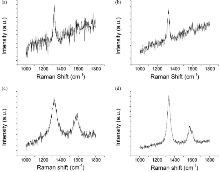
Fig. 3. Raman spectra showing the quality of diamond deposited at different CH4 concentration. (a) 2.5, (b) 5, (c) 10, and (d) 25%.
Fig. 2. The variation of diamond nucleation density with CH4
concen-tration.
are formed to a certain level, their spacing is reduced so that excess carbon species may easily diffuse to those al-ready formed nuclei rather than formed new ones. Similar behavior has been observed on Si by other works [10,11]. The effect of CH4concentration on diamond quality is also investigated. Fig. 3 exhibits the Raman spectra. As can be seen in these spectra, the graphite signal at 1580 cm−1is in-creased with CH4concentration. Also, the diamond peak is wider as CH4concentration is higher. Therefore, the quality of deposited diamond is decreased as CH4concentration is increased. Therefore, it is likely that the increase of density is mainly due to CH4concentration though the bias appli-cation may have a slight effect. The distribution of diamond particles is relatively uniform over the whole area of copper,
Fig. 4. SEM micrographs showing the effect of bias voltage on diamond nucleation with 5% CH4. (a) 0, (b)−150, (c) −200, (d) −250, (e) −300, and
(f)−350 V.
while the central region has slightly higher density than the surroundings. This is in contrast with the case of diamond nucleation on Si substrate in which uniformity of diamond distribution is poor. This is related to the distribution of elec-trical field during biasing. It is speculated that the reflection of microwave on Cu surface might be the reason.
The Cu surface after diamond deposition shows a number of holes, probably caused by hydrogen plasma etching or melting. Interestingly, these holes are not the nucleation sites for diamond.
3.2. Bias voltage effect
The bias voltage effect is studied in the range of 0 to −350 V on the substrates with constant CH4concentration at 5%. The SEM image in Fig. 4 shows that at 0 V bias the nucleation density of diamond is very low, approximately
3×104cm−2. At−150 V, the density is increased about one order of magnitude. Increasing the bias voltage to −200 V resulted in more nucleation on Cu surface. Further increas-ing the bias voltage beyond−250 V, it is seen the density is decreased. Fig. 5 shows the variation of the nucleation den-sity with bias voltage in which it is seen the denden-sity reaching the maximum value of 106cm−2 at−250 V. Similar trend in the cases of diamond deposition on Si has been observed in a study of the effect of bias voltage on nucleation density [10].
In BEN, it has been proposed that the ion energy has to be large than a threshold value which is about 50–80 eV for the deposition on Si [12]. Therefore, the bias voltage has to be raised to see the enhanced nucleation of diamond. If the bias voltage is too high, the ions with sufficient energy to bombard the surface can etch the nuclei, which then reduces the density. In addition, the ion flux has been shown to
Fig. 5. Nucleation density vs. bias voltage with 5% CH4.
increase with bias voltage [12], which might cause etching as well.
4. Conclusions
Diamond nucleation on Cu can be enhanced by the pretreatment of biasing. It is shown that at−250 V increas-ing CH4concentration during the biasing stage can increase the nucleation density until it reaches 10% where diamond nucleation is almost saturated. For the effect of bias volt-age, a maximum density is found at−250 V with 5% CH4. At higher bias voltage, the density is lower probably due to the etching effect of ions.
Acknowledgements
This work was supported by National Science Council, Taiwan, ROC, under contract of NSC 89-2216-009-006.
References
[1] S. Yugo, T. Kanai, T. Kimura, T. Moto, Appl. Phys. Lett. 58 (1991) 1036.
[2] M. Schreck, R. Hessmer, S. Geier, B. Rauschenbach, B. Stritzker, Diamond Relat. Mater. 3 (1994) 510.
[3] S. Yugo, N. Nakamura, T. Kimura, Diamond Relat. Mater. 7 (1998) 1017.
[4] T.P. Ong, F. Xiong, R.P.H. Chang, C.W. White, J. Mater. Res. 7 (1992) 2429.
[5] N. Jiang, C.L. Wang, J.H. Won, M.H. Jaen, Y. Mori, A. Hatta, T. Ito, T. Sasaki, A. Hiraki, Appl. Surf. Sci. 117/118 (1997) 587. [6] N. Jiang, C.L. Wang, J.H. Won, M.H. Jaen, Y. Mori, A. Hatta, T.
Ito, T. Sasaki, A. Hiraki, Diamond Relat. Mater. 6 (1997) 743. [7] S. Ojika, S. Yamashita, K. Kataoka, T. Ishikura, Jpn. J. Appl. Phys.
32 (1993) L200.
[8] S.D. Wolter, B.R. Stoner, G.H.M.Ma, J.T. Glass, in: Proceedings of the MRS Symposium, Vol. 270, 1993, pp. 347–352.
[9] N. Ali, W. Ahmed, C.A. Rego, Q.H. Fan, J. Mater. Res. 15 (2000) 593.
[10] J. Gerber, S. Sattel, H. Ehrhardt, J. Robertson, P. Wurzinger, P. Pongratz, J. Appl. Phys. 78 (1996) 4388.
[11] M. Katoh, M. Aoki, H. Kawarada, Jpn. J. Appl. Phys. 33 (1994) L194.
[12] Sz. Kátai, Z. Tass, Gy. Hárs, P. Deák, J. Appl. Phys. 86 (1999) 5549.