國 立 交 通 大 學
電信工程研究所
博 士 論 文
具低阻抗及強耦合之改良微帶線
及被動元件之應用
Modified Microstrip Lines with Low
Impedance and Enhanced Coupling for
Applications in Passive Circuits
研 究 生:梁 正 憲 (Cheng-Hsien Liang)
指導教授:張 志 揚 (Chi-Yang Chang)
具低阻抗及強耦合之改良微帶線
及被動元件之應用
Modified Microstrip Lines with Low Impedance
and Enhanced Coupling for Applications in
Passive Circuits
研究生:梁正憲
Student:
Cheng-Hsien
Liang
指導教授:張志揚 博士 Advisor:
Dr.
Chi-Yang
Chang
國立交通大學
電信工程研究所
博士論文
A Dissertation
Submitted to Institute of Communication Engineering
College of Electrical and Computer Engineering
National Chiao Tung University
in Partial Fulfillment of the Requirements
for the Degree of Doctor of Philosophy
in
Communication Engineering
Hsinchu, Taiwan
i
具低阻抗及強耦合之改良微帶線及被動元件之應用
研究生:梁正憲 指導教授:張志揚 博士
國立交通大學電信工程研究所
摘要
本論文首先提出一種新的低阻抗微帶線結構,在傳統的微帶線內部加
入接地線,使得微帶線的特性阻抗值可以由在同一平面上的訊號線及接地
線所控制,以此來提升微帶線的等效電容值,使得其特性阻抗值較同樣線
寬的傳統微帶線為低,此種方式對於降低厚基板的特性阻抗值特別顯著,
此外,我們也將訊號線加入至傳統微帶線的地,來更為降低微帶線的特性
阻抗值,將此種微帶線結構應用在四分之一波長的步階阻抗諧振腔上,以
此來製作對製程誤差較不敏感的小型化濾波器,同時也使得濾波器有更小
的尺寸及較寬的上截止帶響應;接著,我們提出了數種可以提供強耦合量
的微帶線耦合結構,分別將其應用在小型化的寬頻濾波器和單節及多節的
3-dB 方向耦合器上,雖然本論文所提出的電路結構需要有較多的導通孔,
但是均可以使用標準的印刷電路板製程在一般的單層基板上完成,因此電
路具有容易製作及低成本的優點。
ii
Modified Microstrip Lines with Low Impedance and
Enhanced Coupling for Applications in Passive Circuits
Student:Cheng-Hsien Liang Advisor:Dr. Chi-Yang Chang
Institute of Communication Engineering
National Chiao Tung University
Abstract
This dissertation first proposes a novel low-impedance microstrip line structure. By inserting ground strips inside the conventional microstrip line, the characteristic impedance of the microstrip line can be controlled by the signal and ground strips in a coplanar manner. Compared to the conventional microstrip line with the same transverse width, the effective capacitance of the microstrip line increases so that the characteristic impedance decreases. The decreasing amount is particularly large for the thick substrate. In addition, we also insert signal strips in the microstrip ground plane to further decrease the characteristic impedance. The low-impedance microstrip line is applied in the quarter-wavelength stepped-impedance resonator. The designed filter can be insensitive to fabrication tolerances and have a smaller size and a wider upper stopband. Then, we propose several coupled microstrip line structures which can provide strong coupling. These tight-coupling structures are used to design miniaturized wideband bandpass filters and single- and multi-section 3-dB directional couplers. Although the proposed circuits need more via-holes, they can be easily fabricated on a single-layer substrate by the conventional printed circuit board (PCB) process with low cost.
iii
誌 謝
在近四年的博士班生涯中,能夠順利取得博士學位,首先要感謝我的指導教授張志 揚博士,從大學三年級開始跟隨老師做專題,將近八年的時間裡,老師不但在專業研究 領域中給我莫大的教導與幫助,而且其豁達樂觀的處世態度,更是我學習的對象,老師 對於大自然及腳踏車的熱愛,讓我在辛苦做研究之餘也可以適時放鬆心情,跟隨老師遊 山玩水;我也要感謝口試委員陳俊雄教授、吳瑞北教授、王暉教授、郭仁財教授、江逸 群教授、湯敬文教授、鍾世忠教授以及孟慶宗教授,他們提供了寶貴的意見及指正,使 論文更加豐富完整。 感謝實驗室博士班共同奮鬥的伙伴們維欣、金雄、益廷、建育、昀緯,祝福你們在 追求夢想的道路上順利,也要感謝歷屆的碩士班學弟妹們鵬達、懿萱、宛蓉、祥容、梓 淳、義傑、仕鈺、弘偉…等,有了大家的陪伴,使得實驗室充滿歡樂的氣氛,讓博士班 的生活增添不少樂趣;我也要感謝求學過程中眾多的好友們翰丞、智仁、勝凱、文傑… 等,以及登山隊的伙伴們俊哥、阿樸、英公、小胖、小花,一路上要感謝的朋友真的太 多了,謝謝大家,有你們的陪伴真好。 我要感謝眾多疼愛我的親人們,有了你們的支持和鼓勵,讓我在求學路上即使遇到 挫折時仍舊充滿信心不放棄,特別是台南年邁的外婆心中一直掛念著我何時才能拿到博 士學位,如今她臉上終於露出了久久不見的笑容;特別感謝維欣在我口試當天一早起來 辛苦為口試委員們所準備的水果,還有在新竹科學園區工作的弟弟正勳特地於百忙之中 請假來幫忙我打理口試的一切,有了你們二位的協助,使得畢業論文口試可以順利圓滿 結束,也謝謝修真在畢業典禮上所贈送親手完成的又大又香的花束,美麗的花朵讓實驗 室飄香芬芳了好幾天,最後,我想將這篇論文,獻給辛苦養育我的父親—梁進通,母親— 梁郭貴滿,讓我可以無後顧之憂完成博士學位。梁正憲 於新竹交大 2011 年 7 月 22 日
iv
Contents
Abstract (Chinese)...i Abstract...ii Acknowledgment...iii Contents...iv List of Tables...vii List of Figures...viii Chapter 1 Introduction...1 1.1 Research motivation...2 1.2 Literature survey...3 1.3 Contribution...6 1.4 Organization ...7Chapter 2 Fundamental theory and design of coupled-resonator filters and coupled lines....9
2.1 Coupled resonator theory...9
2.1.1 Lowpass filter prototype...9
2.1.2 Impedance (K) and admittance (J) inverters...9
2.1.3 Impedance scaling and frequency transformation...12
2.1.4 Reactance and susceptance slope parameters...14
2.1.5 Design equations for coupled-resonator bandpass filters...15
2.1.6 Extraction of the external quality factor and coupling coefficient...16
2.1.7 Chebyshev and quasi-elliptic filters...17
2.2 Resonance properties of the λ/4 SIR...20
2.3 Microstrip line and coupled microstrip lines...22
v
2.3.2 Coupled microstrip lines...24
2.3.3 Coupled line coupler...26
Chapter 3 Novel low-impedance microstrip line for quarter-wavelength stepped-impedance resonator filters...31
3.1 Fabrication-tolerant microstrip quarter-wavelength SIR filter...31
3.1.1 New modified microstrip structure...33
3.1.2 Characteristics of the proposed λ/4 SIR...34
3.1.3 Four-pole cross-coupled filter design...43
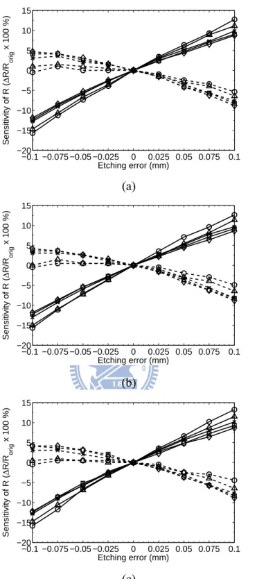
3.1.4 Sensitivity to etching tolerances...49
3.2 Miniaturized microstrip quarter-wavelength SIR filter...55
3.2.1 Analysis of the proposed structure...55
3.2.2 Four-pole cross-coupled filter design...57
3.3 Resonance of the low-impedance section of the SIR...62
3.4 Discussion of the number of via-holes...67
3.5 Summary...69
Chapter 4 Interdigital coupling structures for wideband stepped-impedance resonator filters.. ...70
4.1 Interdigital coupled microstrip lines...70
4.2 Proposed SIR configuration I...71
4.2.1 Structure of the resonator...71
4.2.2 Four-pole Chebyshev filter (filter I)...72
4.2.3 Four-pole generalized Chebyshev filter (filter II)...77
4.2.4 Resonance of the circumference of the low-impedance section...79
4.3 Proposed SIR configuration II...82
4.3.1 Structure of the resonator...82
vi
4.4 Summary...91
Chapter 5 Enhanced coupling structures for tight couplers and wideband filters...92
5.1 Proposed coupled-line structures...93
5.1.1 Type I...93
5.1.2 Type II...98
5.2 Wideband quarter-wavelength parallel-coupled filter...101
5.3 Wideband quarter-wavelength hairpin filter...107
5.4 Single-section 3-dB directional coupler...112
5.5 Three-section 3-dB directional coupler...118
5.6 Five-section 3-dB directional coupler...123
5.7 Summary...129
Chapter 6 Conclusion and future works...131
6.1 Conclusion...131
6.2 Future works...132
vii
List of Tables
Table 3-1 Characteristic impedance (Ω) for different numbers of inserted ground strips (Total
line width is kept constant as 3 mm.)...34
Table 3-2 Design parameters of the proposed SIR filters...43
Table 3-3 Dimensions of the designed filters...45
Table 3-4 Comparison of measured passband insertion losses for the conventional and propo- sed SIR filters...50
Table 3-5 Sensitivity to etching tolerances in terms of the percentage deviation of the center frequency for the conventional and proposed SIR filters...54
Table 3-6 Characteristic impedance (Ω) of the conventional and proposed microstrip lines... ...57
Table 3-7 Design parameters of the proposed SIR filters...58
Table 3-8 Dimensions of the designed filters...59
Table 3-9 Fabricated filters and measured results...62
Table 5-1 Dimensions (in millimeters) of the three-section directional coupler...120
Table 5-2 Design parameters of the five-section directional coupler...123
viii
List of Figures
Fig. 1-1. Cross-sectional view of the conventional microstrip line...3
Fig. 1-2. Cross-sectional views of the symmetric coupled microstrip lines. (a) Conventional. (b) Modified with the ground-plane aperture...4
Fig. 2-1. Lowpass filter prototypes and their element definitions. (a) Prototype beginning with a shunt element. (b) Prototype beginning with a series element...10
Fig. 2-2. Lowpass filter prototypes with (a) K-inverters and (b) J-inverters...11
Fig. 2-3. Bandpass filters using (a) K-inverters and (b) J-inverters...13
Fig. 2-4. Generalized bandpass filters with distributed elements and (a) K-inverters. (b) J-in- verters...15
Fig. 2-5. (a) Phase response of S11 for the input and output coupling structures. (b) Resonant response of the coupled resonator pair...17
Fig. 2-6. (a) Coupling diagram and (b) frequency response for the four-pole Chebyshev filter. ...18
Fig. 2-7. (a) Coupling diagram and (b) frequency response for the four-pole quasi-elliptic filter...20
Fig. 2-8. (a) Conventional λ/4 microstrip SIR. (b) Normalized length and (c) normalized spurious frequency versus impedance ratio for θ θ1= ...21 2 Fig. 2-9. Capacitance representation of a conventional microstrip line...23
Fig. 2-10. Quasi-TEM modes of the conventional coupled microstrip lines. (a) Even mode. (b) Odd mode...24
Fig. 2-11. Single-section microstrip coupled line coupler...26
Fig. 2-12. Equivalent circuit for the even-odd mode analysis...26
ix
Fig. 3-1. (a) Conventional λ/4 microstrip SIR. Dashed lines represent etching errors. (b) Nor- malized resonant frequency versus the percentage variation of the impedance ratio. ...32 Fig. 3-2. (a) Top view of the proposed microstrip structure. (b) Cross-sectional view of the cir- cled portion in (a)...33 Fig. 3-3. (a) Proposed λ/4 microstrip SIR. (b) Comparison of the frequency responses of the resonators with one and two via-holes on the ends of each inserted ground strip.... ...35 Fig. 3-4. Impedance ratio R of the conventional and proposed λ/4 SIRs versus substrate thick- ness h and width WL (in millimeters) for: (a) εr =3.6, (b) εr =6.8, and (c)
10.2 r
ε = . Conventional: solid line. Proposed: dashed line. (circle ○: 1.35,WL =
1
N = ; triangle △: 2.4, WL = N = ; cross ×: 3.45, 2 WL = N = ; asterisk *: 3 4.5, 4
L
W = N = ; square □: 5.55, WL = N = ; diamond ◇: 6.6, 5 WL = N = .).. 6 ...37 Fig. 3-5. Impedance ratio R versus substrate thickness h for the proposed λ/4 SIRs with differ- ent numbers of inserted ground strips when WL =3.45 mm. (a) εr =3.6. (b)
6.8 r
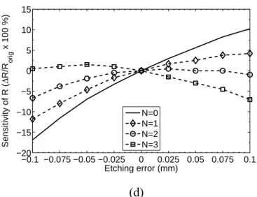
ε = . (c) εr =10.2. (N: number of inserted ground strips. N =0: conventional microstrip structure.)...38 Fig. 3-6. Sensitivity to etching tolerances for the conventional and proposed λ/4 SIRs with various values of the substrate thickness h (in millimeters) when WL =3.45 mm. (a) 3.6εr = . (b) εr =6.8. (c) εr =10.2. Conventional: solid line. Proposed (N =3): dashed line. Positive: under-etching. Negative: over-etching. (circle ○:
0.5
h= ; triangle △: h=0.625; cross ×: h=1; square □: h=1.25; diamond ◇: h=1.5.)...40 Fig. 3-7. Sensitivity to etching tolerances for the proposed λ/4 SIRs with different numbers
x 0.225
H
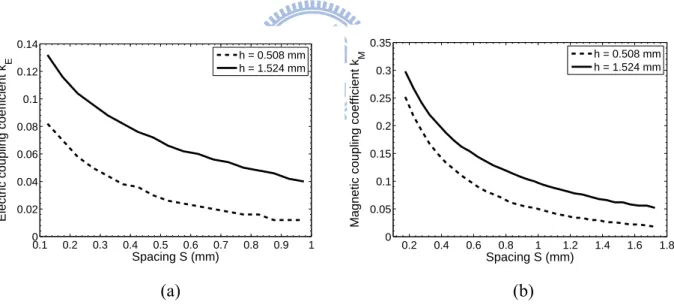
W = mm. Case II: WL =3.4 mm, WSI =WI =0.25 mm, WG =0.275 mm, and WH =0.175 mm.) (a) Case I: h=0.5 mm. (b) Case I: h=1.5 mm. (c) Case II: h=0.5 mm. (d) Case II: h=1.5 mm. (N: number of inserted ground strips. N =0: conventional microstrip structure.)...43 Fig. 3-8. Coupling structures for: (a) electric coupling and (b) magnetic coupling...45 Fig. 3-9. Coupling coefficients of the coupling structures for: (a) electric coupling and (b)
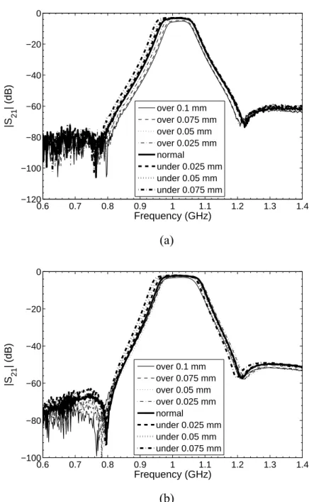
magnetic coupling...45 Fig. 3-10. Proposed layout of the four-pole cross-coupled filter...46 Fig. 3-11. Photograph of the fabricated circuit (filter I)...46 Fig. 3-12. Simulated (dashed line) and measured (solid line) results (|S11| and |S21|) of filter I.
(a) Narrowband responses. (b) Wideband responses...47 Fig. 3-13. Photograph of the fabricated circuit (filter II)...48 Fig. 3-14. Simulated (dashed line) and measured (solid line) results (|S11| and |S21|) of filter II.
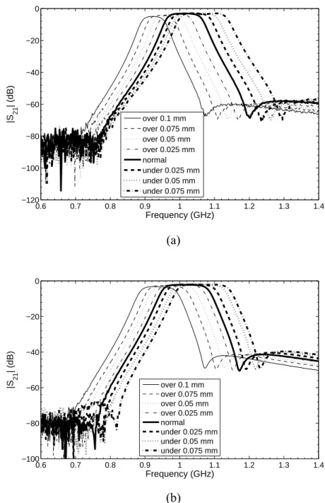
(a) Narrowband responses. (b) Wideband responses...49 Fig. 3-15. Current distribution of the proposed filter at the center frequency...50 Fig. 3-16. Measured sensitivity to etching tolerances for the proposed SIR filter. (a) Filter I. (b) Filter II (over: over-etching; under: under-etching)...51 Fig. 3-17. Measured sensitivity to etching tolerances for the conventional SIR filter (WL and WH are the same as those of the proposed filter). (a) Filter I. (b) Filter II (over: over-etching; under: under-etching)...52 Fig. 3-18. Measured sensitivity to etching tolerances for the conventional SIR filter (R and WH
are the same as those of the proposed filter). (a) Filter I. (b) Filter II (over: over- etching; under: under-etching)...53 Fig. 3-19. Proposed microstrip structure. (a) Top view. (b) Bottom view. (c) Cross-sectional view...56 Fig. 3-20. Proposed λ/4 microstrip SIR...57
xi
Fig. 3-21. Proposed layout of the four-pole cross-coupled filter...58 Fig. 3-22. (a) Top view (left side) and bottom view (right side) of the fabricated filter I. (b) Narrowband responses. (c) Wideband responses. (simulation: dashed line; mea- surement: solid line.)...60 Fig. 3-23. (a) Top view (left side) and bottom view (right side) of the fabricated filter II. (b) Narrowband responses. (c) Wideband responses. (simulation: dashed line; mea- surement: solid line.)...61 Fig. 3-24. Resonant response of the proposed SIR in Section 3.1...62 Fig. 3-25. Current distributions of the resonances (a) fp1 and (b) fp2 in Fig. 3-24. Elimination of
the resonances of the circumference via (c) a bond-wire or (d) a signal strip on the bottom layer...64 Fig. 3-26. (a) Current distribution of the resonance fp3 in Fig. 3-24. Elimination of the reso- nance fp3 via (b) two bond-wires or (c) two signal strips on the bottom layer... ...64 Fig. 3-27. (a) Current distribution of the resonance fp4 in Fig. 3-24. Elimination of the reso- nance fp4 via three via-holes and (b) a bond-wire or (c) a signal strip on the bottom layer...65 Fig. 3-28. SIR with three via-holes on each inserted ground strip and either (a) a bond-wire or (b) a signal strip on the ground plane to eliminate unwanted resonances. (c) Resonant response of the SIR in (a) or (b) ...66 Fig. 3-29. Current distributions of the resonances (a) f1, (b) f2, and (c) f3 in Fig. 3-28...67
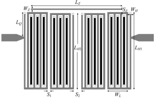
Fig. 3-30. (a) SIRs with one to five via-holes on each inserted ground strip. (b) Comparison of the resonant responses of the SIRs in (a) ...68 Fig. 4-1. Two interdigital coupling structures for wideband filter design...71 Fig. 4-2. Proposed λ/4 SIR configuration I. (a) Top view. (b) Bottom view (N=2)...72 Fig. 4-3. Configuration of the proposed filter I. (a) Top-layer layout. (b) Bottom-layer layout.
xii
Filter Dimensions (in millimeters): LQ =11.9, LH1=14.45, LH2 =13.525, LC =
12.5, 3.25LM = , 0.25WH =WC = , 3.45WL = , 1.05WS = , and S d= =0.15.... ...73 Fig. 4-4. Design curves for the proposed filter I. (a) External quality factor Qe. (b) Electric coupling k12 and k34. (c) Magnetic coupling k23...75
Fig. 4-5. Top view (left side) and bottom view (right side) of the fabricated filter I...76 Fig. 4-6. Simulated (dashed line) and measured (solid line) results of filter I. (a) Scattering parameters. (b) Passband group delay...77 Fig. 4-7. Configuration of the proposed filter II. (a) Top-layer layout. (b) Bottom-layer layout. units: mm...78 Fig. 4-8. Top view (left side) and bottom view (right side) of the fabricated filter II...79 Fig. 4-9. Simulated (dashed line) and measured (solid line) results of filter II. (a) Scattering parameters. (b) Passband group delay...80 Fig. 4-10. (a) Current distribution of the resonance of the circumference. (b) Elimination of the resonance in (a)...81 Fig. 4-11. Proposed λ/4 SIR configuration II...82 Fig. 4-12. Normalized first spurious resonant frequency versus finger number N, finger length
LF, and width WL...83 Fig. 4-13. Coupling structures for: (a) electric coupling and (b) magnetic coupling...84 Fig. 4-14. Proposed layout of filter I. units: mm...85 Fig. 4-15. Coupling coefficients of the coupling structures for: (a) electric coupling and (b) magnetic coupling...86 Fig. 4-16. Photograph of the fabricated filter I...86 Fig. 4-17. Simulated (dashed line) and measured (solid line) results of filter I. (a) Scattering parameters. (b) Passband group delay...87
xiii
Fig. 4-18. Proposed layout of filter II. units: mm...88 Fig. 4-19. Photograph of the fabricated filter II...89 Fig. 4-20. Simulated (dashed line) and measured (solid line) results of filter II. (a) Scattering parameters. (b) Passband group delay...90 Fig. 5-1. Proposed coupled microstrip lines of type I. (a) Top view. (b) Bottom view. (c)
Cross-sectional view...93 Fig. 5-2. Quasi-TEM modes of the proposed coupled microstrip lines (type I). (a) Even mode. (b) Odd mode...95 Fig. 5-3. Coupling factor C versus microstrip line width W for two aperture sizes WR =1.65
mm (circle ○) and 2.85 mm (triangle △). Conventional (Fig. 1-2(a)): dashed- dotted line. Modified with the ground-plane aperture (Fig. 1-2(b)): dashed line. Proposed: solid line...96 Fig. 5-4. Comparison of the coupling factor C for three different coupled lines with two aper- ture sizes WR =1.65 mm (circle ○) and 2.85 mm (triangle △). Structure in [62]: dashed-dotted line. Proposed without via-holes: dashed line. Proposed with via- holes: solid line...98 Fig. 5-5. Proposed coupled microstrip lines of type II. (a) Top view. (b) Bottom view. (c)
Cross-sectional view...99 Fig. 5-6. Quasi-TEM modes of the proposed coupled microstrip lines (type II). (a) Even
mode. (b) Odd mode...100 Fig. 5-7. Comparison of the (a) even- and odd-mode impedances (Ze, Zo) and (b) coupling factor C versus microstrip line width W for types I (dashed line) and II (solid line) with two aperture sizes WR =1.65 mm (circle ○) and 2.85 mm (triangle △) ... ...101 Fig. 5-8. Even- and odd-mode impedances (Ze, Zo) and effective dielectric constants (εree, εreo) versus normalized values W/h, WR/h, WS/h, S/h, SG/h, and SR/h. (a) W hR/ =3.5,
xiv
/ G/ 0.5
S h S= h= , and (WS +SR) /h=1.5. (b) W hR / =4.1, /S h S= G/h=0.5, and (WS +SR) /h=1.8. (c) W hR/ =4.1, /S h S= G/h=1.1, and (WS +SR) /h=1.5 ...103 Fig. 5-9. Configuration of the four-pole λ/4 parallel-coupled filter. (a) Top-layer layout. (b) Bottom-layer layout. Filter dimensions: L1=22.8 mm, L2 =4.8 mm, L3 =2.35 mm, 1.55LQ = mm, LM =6.55 mm, LS1 =21.9 mm, S1=SG =0.55 mm,
0.15 T
S = mm, SR =0.25 mm, W =1.1 mm, WS =0.5 mm, and WT =0.3 mm ...104 Fig. 5-10. Top view and bottom view of the fabricated λ/4 parallel-coupled filter...105 Fig. 5-11. Simulated (dashed line) and measured (solid line) results of the λ/4 parallel-coupled filter. (a) Scattering parameters. (b) Passband group delay...106 Fig. 5-12. Measured sensitivity to etching tolerances for the λ/4 parallel-coupled filter (over: over-etching; under: under-etching) ...106 Fig. 5-13. Proposed λ/4 hairpin resonator. (a) Top view. (b) Bottom view...108 Fig. 5-14. Coupling structures and design curves for the proposed λ/4 hairpin filter. (a) Elec- tric coupling and (b) magnetic coupling...109 Fig. 5-15. Configuration of the proposed four-pole λ/4 hairpin filter. (a) Top-layer layout. (b) Bottom-layer layout. Filter dimensions: L1=15.5 mm, L2 =2.5 mm, L3 =
14.35 mm, LQ =11.1 mm, LM =1.65 mm, LS1=14.6 mm, LS2 =13.45 mm,
0.75
W = mm, WS =0.3 mm, and S1=S2 =SR =SG =0.15 mm...110 Fig. 5-16. Top view (left side) and bottom view (right side) of the fabricated λ/4 hairpin filter. ...111 Fig. 5-17. Simulated (dashed line) and measured (solid line) results of the λ/4 hairpin filter. (a) Scattering parameters. (b) Passband group delay...112 Fig. 5-18. Even- and odd-mode impedances (Ze, Zo) and effective dielectric constants (εree,
xv
εreo) versus normalized values W/h, WR/h, WS/h, S/h, SG/h, and SR/h. (a) / 4.1 R W h= , /S h S= G/h=0.3, a n d (WS +SR) /h=1.9. ( b ) W hR/ =4.7, / G/ 0.3 S h S= h= , and (WS +SR) /h=2.2. (c) W hR/ =4.4, /S h S= G/h=0.6, and (WS +SR) /h=1.9...114
Fig. 5-19. Configuration of the proposed 3-dB coupler. (a) Top-layer layout. (b) Bottom-layer layout. Coupler dimensions: L1 =35.95 mm, L2 =33.75 mm, LS1=32.85 mm, LS2 =31.5 mm, S1=S2 =ST =SG =0.15 mm, SR =0.5 mm, W =0.75 mm, 0.6WS = mm, WT =0.3 mm, and WR =0.15 mm...115
Fig. 5-20. Top view and bottom view of the fabricated coupler...115
Fig. 5-21. Simulated (dashed line) and measured (solid line) results of the coupler. (a) In- sertion losses |S21| and |S31|. (b) Return loss |S11| and isolation |S41|. (c) Phase differ- ence between the coupled and through ports...117
Fig. 5-22. Measured sensitivity to etching tolerances for the proposed 3-dB coupler (over: over-etching; under: under-etching) ...118
Fig. 5-23. Schematic of the tight-coupling section (section 2) ...119
Fig. 5-24. Design chart for the tight-coupling section with S=0.15 mm...119
Fig. 5-25. Simulated response of the proposed three-section directional coupler...120
Fig. 5-26. Top view and bottom view of the fabricated three-section directional coupler... ...121
Fig. 5-27. Measured response of the three-section directional coupler...121
Fig. 5-28. Simulated and measured amplitude and phase imbalances between the coupled and through ports. (a) Amplitude imbalance. (b) Phase imbalance...122
Fig. 5-29. Cross-sectional view of the enhanced coupling structure in sections 2 and 4... ...123 Fig. 5-30. Even- and odd-mode impedances (Ze, Zo) and effective dielectric constants (εre, εro) versus normalized values S/h and W/h for SR/h=0.3 and W hS / =0.6. (a)
xvi
Even-mode. (b) Odd-mode...125 Fig. 5-31. Cross-sectional view of the enhanced coupling structure in section 3...125 Fig. 5-32. Even- and odd-mode impedances (Ze, Zo) and effective dielectric constants (εre, εro) versus normalized values W/h and WR/h for S h/ =0.3. (a) Even-mode. (b) Odd- mode...126 Fig. 5-33. Top view and bottom view of the fabricated five-section directional coupler...
...127 Fig. 5-34. Simulated result of the five-section directional coupler...128 Fig. 5-35. Measured result of the five-section directional coupler...128 Fig. 5-36. (a) Amplitude difference between the coupled and through ports. (b) Phase differ- ence between the coupled and through ports...129
1
Chapter 1 I
NTRODUCTION
A microstrip line is one of the most popular transmission lines and plays an important role in commercialized portable devices and microwave systems. The advantages of a mi- crostrip line are: 1) planar structure; 2) easy fabrication by photolithographic processes for low cost; and 3) easy integration with passive and active microwave devices. Due to the rapid growth in modern wireless communication systems, passive components such as filters, directional couplers, and etc., are largely constructed by a microstrip line for easy integration into the printed circuit board (PCB). However, fabrication tolerances and limitations in the conventional PCB process seriously limit the application of a microstrip line.
Filters are essential components in microwave systems. The trend of bandpass filters (BPFs) is toward compact size, low cost, high selectivity, and wide stopband. Another important issue regarding the narrowband filter design is the low sensitivity to fabrication tolerances, especially for some resonator structures. Recently, wideband communication systems attract much attention for the high data-rate capacity. To design passive components for wideband applications, tightly coupled lines are usually required to obtain strong coupling. Generally speaking, due to fabrication limitations, it is difficult to implement a microstrip filter with the fractional bandwidth larger than 20% and a microstrip directional coupler with a 3-dB coupling on a commonly used single-layer substrate (for example, a RO4003 substrate with a dielectric constant of 3.58 and a thickness of 0.508 mm). In this chapter, we discuss the difficulties to realize fabrication-tolerant filters, wideband filters, and tightly coupled lines using the conventional microstrip line and coupled microstrip lines. Previous studies for compact filters, wideband filters, and tight couplers are described and summarized. Finally, we give an outline of this dissertation.
2
1.1 Research Motivation
High performance BPFs have become more and more important in recent years due to the rapid growth in modern wireless communication systems. The microstrip filter plays an important role in modern filter applications due to its planar structure and suitability for circuit integration. Recently, the stepped-impedance resonator (SIR) filter has been a hot topic because of its ability to reduce the circuit size and to improve the upper stopband performance. Theoretical analysis reveals that the fundamental frequency and the first spurious frequency of the SIR are mainly controlled by the impedance ratio of the high- and low-impedance line sections. As a result, small fabrication errors may cause a large variation of the impedance ratio, which will degrade the filter performance seriously. Although numerous studies have been performed on the advantages of SIRs, how to decrease the effect of fabrication tolerances is still critically lacking.
Next generation wireless systems and high data-rate communication systems require wideband components. However, it is difficult to achieve moderate to tight coupling in the conventional coupled microstrip lines due to the minimum allowable line width and gap spacing. This causes a challenge to design wideband BPFs and tight couplers. In addition, for wideband BPFs, the first spurious frequency should be far apart from the center frequency, or the stopband rejection may be poor. Therefore, strong coupling strength and wide spurious- free performance are the two challenges to design small wideband BPFs. On the other hand, a directional coupler with a 3-dB coupling is usually required in practical applications. The high even-mode impedance and the low odd-mode impedance lead to the very narrow line width and gap spacing, especially for the multisection 3-dB directional coupler.
This dissertation is to demonstrate several novel microstrip lines and coupled microstrip lines to overcome the drawbacks described above. Fabrication-tolerant filters, small wideband filters, and 3-dB directional couplers are experimented on the basis of the proposed structures.
3
Fig. 1-1. Cross-sectional view of the conventional microstrip line.
In addition, to facilitate the implementation process and to minimize the fabrication cost, all the circuits should be able to realize on a single-layer substrate by the conventional PCB process.
1.2 Literature Survey
A microstrip line, as shown in Fig. 1-1, supports a quasi-TEM mode of propagation and is widely applied to design microwave circuits, such as filters, couplers, and etc. The mi- crostrip parallel-coupled filter proposed by Cohn [1] in 1958 has been extensively used in the microwave area because of its planar structure, insensitivity to fabrication tolerances, and well-known synthesis method. However, there are two drawbacks limiting the application of this type of filter. One is that the whole length of the filter is too long as the order of the filter becomes high. The other is that due to the unequal even- and odd-mode phase velocities, it suffers from the existence of the spurious response at 2f0 (i.e., twice the center frequency),
which may cause a poor attenuation level in the stopband [2].
SIR filters have been proposed to solve the drawbacks mentioned above [3]-[17]. They can be categorized into three major types, namely: 1) quarter-wavelength; 2) half-wavelength; and 3) one-wavelength SIR filters. The resonant frequency of the SIR is primarily controlled by the impedance ratio of the line sections. For the same substrate, the characteristic impe- dance of the conventional microstrip line is only controlled by the width of the conductor.
4
(a) (b)
Fig. 1-2. Cross-sectional views of the symmetric coupled microstrip lines. (a) Conventional. (b) Modified with the ground-plane aperture.
Due to the restriction of the fabrication process, manufacturing tolerances may influence the performance of the filter and cause a shift of the center frequency. These effects are much more obvious on the SIR than on the uniform-impedance resonator (UIR). This is because for a constant amount of etching error on the conventional microstrip line, the percentage width variation (i.e., etching error divided by the normal width in percent) in the high-impedance section is much larger than that in the low-impedance section. Thus, the variation of the characteristic impedance of the high-impedance line is different from that of the low- impedance line, and this may cause the impedance ratio of the SIR to change largely. Thereby, the conventional microstrip SIR is very sensitive to fabrication tolerances. However, until now, there is still no works related to the sensitivity of microstrip SIR filters.
Coupled microstrip lines are extensively used to design directional couplers and edge- coupled filters. Tightly coupled directional couplers (especially a 3-dB coupler) and wideband filters are essential components in modern wireless communication systems. For the tight coupler and wideband filter design, strongly coupled microstrip lines [see Fig. 1-2(a)] are required. Nonetheless, the minimum line width and gap spacing in the conventional PCB process are only approximately 0.15 mm. On the other hand, most of the popularly used PCBs have low dielectric constants. It is inherently difficult to implement tightly coupled lines with low-dielectric-constant substrates.
5
Various approaches have been proposed to design a single-section 3-dB coupler. The most famous one is the Lange coupler [18]-[20], which is used extensively in the monolithic microwave integrated circuit (MMIC). However, the line width and gap spacing for either a four- or six-line 3-dB Lange coupler will be far below the fabrication limitation of the PCB process if a common substrate (for example, a RO4003 substrate with a dielectric constant of 3.58 and a thickness of 0.508 mm) is used. The vertically installed planar (VIP) structure [21], [22] could fit the PCB process, but it needs some special tools to solder the vertical substrate. The multilayer structure [23]-[27] requires multilayer substrates. A floating conductor along with a small dielectric layer [28]-[30] can be placed above the signal strips or between the signal strips and the microstrip ground plane. All the structures in [23]-[30] lead to higher fabrication costs compared to a single-layer substrate structure. A 3-dB coupler can also be fabricated on a single-layer substrate with broadside-coupled structures employing coplanar waveguides (CPWs) [31], [32]. Nevertheless, these structures may have the input and output ports on different sides of the substrate and might be difficult to apply to wideband filter design. Since there must be ground plane metals on two sides of the top layer, filter topologies such as interdigital, combline, or hairpin filters are not suitable.
Since broadband communication systems (e.g., ultra-wideband (UWB) system) are highly developed, multisection 3-dB directional couplers are necessary to increase the band- width. It is much more difficult to implement a multisection 3-dB directional coupler on the PCB since a very high even-mode impedance and a very low odd-mode impedance are required for the extremely tight-coupling inner sections. Although the Lange coupler [33] and the tandem coupler [34] have been used to design the tight-coupling section of a three-section 3-dB directional coupler, they require wire crossovers and may be unable to achieve very tight coupling on the low-dielectric-constant substrate. Thus, they are not appropriate to realize the tight-coupling section of a multisection directional coupler. The broadside-coupled and slot-coupled approaches can be applied to construct very tight-coupling structures [35]-[40],
6
but they require multilayer substrates. The VIP structure has been used in the tight-coupling sections to design a five-section directional coupler with a wide bandwidth of 160% [41]. As mentioned above, it is complicated from the manufacturing point of view.
To design a microstrip, wideband, coupled-resonator BPF on the PCB, there are many published works. The ground-plane aperture technique and the defected ground structure (DGS), as shown in Fig. 1-2(b), are commonly used to enhance the coupling [42]-[44]. In Fig. 1-2(b), the aperture width WR varies according to the required coupling strength. Dual-plane and broadside-coupled structures [45]-[48] enable the stronger coupling, and filters with these structures inherently exhibit wideband characteristics. Other techniques, such as multilayer structures [30], [49], three-line microstrips [50], multimode resonators [51], [52], the cascade of lowpass and highpass filters [53], and the new coupling scheme in [54] are used to design wideband BPFs. However, the above-mentioned filters may be large, require multilayer technology, or have a narrow upper stopband. To summarize, it is more appropriate to design new coupling structures suitable for tight couplers, wideband filters, and other circuits that require strong coupling.
1.3 Contribution
In this dissertation, we propose a new microstrip line with the signal and ground strips on the same plane. Accordingly, the characteristic impedance of the proposed microstrip line can be controlled by the signal and ground strips in a coplanar manner, in addition to the total line width and substrate thickness. The proposed microstrip line is easily adopted in the low- impedance section of the SIR not only to reduce the resonator size but also to decrease the sensitivity of dimensional errors of the SIR. As a result, the SIR filter has a further smaller size and is insensitive to fabrication tolerances.
7
section of the SIR is modified to have parallel thin strips. Since the magnetic coupling is much stronger than the electric coupling and can be increased easily by a short-circuited stub, it is much less constrained. The purpose of the thin strips in the low-impedance section of the SIR is to obtain a strong interdigital coupling between adjacent SIRs. Consequently, the filter can have a compact size, a wide passband, and a wide upper stopband.
Two novel microstrip coupling structures are also proposed to solve the coupling strength problem of the conventional coupled microstrip lines. The proposed coupled-line structures both have a rectangular ground-plane aperture and two inserted signal strips in the aperture to increase the coupling strength significantly. The proposed two structures have good compatibility with the conventional coupled microstrip lines so that they are applied to implement the single- and multi-section directional couplers. In addition, since these two coupling structures are easily adopted in any part of the resonator where the strong coupling is required, they are used to design wideband BPFs. All the proposed circuits can be fabricated on a single-layer substrate by the conventional PCB process.
1.4 Organization
This dissertation is organized as follows. Chapter 1 describes the conventional microstrip line and coupled microstrip lines, together with their difficulties to design some microwave components. Chapter 2 introduces the basic filter prototypes and coupled-resonator circuits for BPFs. The theory of the microstrip parallel coupled line coupler is also expressed.
In Chapter 3, a novel microstrip structure is proposed to design miniaturized filters. The proposed microstrip line has another degree of freedom to control the characteristic impe- dance. It is easily incorporated in the conventional microstrip SIR not only to reduce the resonator size but also to decrease its sensitivity to fabrication tolerances. The concepts and characteristics of the modified resonator structure are discussed in detail. The filters con-
8
structed by the conventional microstrip SIR are also designed and fabricated to compare with the proposed filters.
In Chapter 4, we propose two interdigital coupling structures to design several wideband SIR BPFs. Generally speaking, it is very difficult to design small wideband BPFs since the coupling strength would be too weak for small-size resonators, especially for a SIR. However, the SIR has a high spurious frequency so that it is very appropriate for wideband filter design. Here, compact wideband BPFs are developed by modifying the low-impedance section of the SIR. With a proper coupling scheme, the coupling strength between adjacent resonators can be very large so as to design small wideband SIR BPFs.
In Chapter 5, two novel enhanced coupling structures are presented to achieve moderate to tight coupling. The proposed two coupling structures have many physical parameters for design flexibility to meet practical applications. These two coupling structures only require a single-layer substrate. No fine lines and narrow gaps are required so as to fit the conventional PCB process. In addition, they are both compatible with the conventional microstrip line and coupled microstrip lines. Therefore, we design several 3-dB directional couplers and wide- band filters by combining the conventional and proposed microstrip structures.
9
Chapter 2 F
UNDAMENTAL
T
HEORY
AND
D
ESIGN
OF
C
OUPLED-
R
ESONATOR
F
ILTERS
AND
C
OUPLED
L
INES
This chapter focuses on the theory of coupled resonator circuits and symmetric microstrip parallel coupled lines. These are the two basic topics for the design of microstrip filters and couplers in this dissertation. In addition, the coupling schemes of the Chebyshev and quasi-elliptic filters are illustrated. The characteristics of the λ/4 stepped-impedance resonator (SIR) are also discussed since it is used in the proposed filter design.
2.1 Coupled Resonator Theory
In 1951, Dishal [55], [56] proposed an approach to design any lumped-element or distributed bandpass filter (BPF) by three parameters: 1) the resonator frequency, f0; 2) the
coupling between adjacent resonators, k; and 3) the external quality factor, Qe. Afterwards, this approach is summarized by Hong and Lancaster [57].
2.1.1 Lowpass Filter Prototype
For the filter design, it is usually from the ladder circuits for lowpass filter prototypes, as shown in Fig. 2-1, with a source resistance or conductance equal to one (i.e., g0 = ) and a 1 cutoff frequency Ω = . Both the circuits in Fig. 2-1 give the same response. The element c 1 values gi, i=1 to n, represent a series inductor or a shunt capacitor. gn+1 is a load resistance or conductance. The element values of the lowpass filter prototypes can be tabulated as long as the filter specifications are given.
2.1.2 Impedance (K) and Admittance (J) Inverters
10 (a)
(b)
Fig. 2-1. Lowpass filter prototypes and their element definitions. (a) Prototype beginning with a shunt element. (b) Prototype beginning with a series element.
series or shunt elements to implement filters. The K- or J-inverter is a two-port network. Ideally, the inverter parameter is frequency invariable. The ABCD matrix of an ideal
K-inverter is 0 1 0 jK A B C D jK ⎡ ⎤ ⎡ ⎤ ⎢ ⎥ = ⎢ ⎥ ⎢± ⎥ ⎣ ⎦ ⎢ ⎥ ⎣ ⎦ m (2.1)
where K is a real value and is defined as the characteristic impedance of the inverter. Thereby, for a K-inverter terminated with an impedance Z2, the impedance Z1 seen from the other port
of a K-inverter is 2 1 2 K Z Z = . (2.2)
11 (a)
(b)
Fig. 2-2. Lowpass filter prototypes with (a) K-inverters and (b) J-inverters.
It is seen that if Z2 is inductive, Z1 becomes capacitive, and vice versa. The inverter has a
phase shift of ±90○.
The ABCD matrix of an ideal J-inverter is
1 0 0 A B jJ C D jJ ⎡ ± ⎤ ⎡ ⎤ ⎢ ⎥ = ⎢ ⎥ ⎢ ⎥ ⎣ ⎦ ⎢ ⎥ ⎣m ⎦ (2.3)
where J is a real value and is defined as the characteristic admittance of the inverter. Again, if a J-inverter is terminated with an admittance Y2, the input admittance Y1 seen looking in the
other port is 2 1 2 J Y Y = . (2.4)
12
Apparently, a J-inverter has the same property as a K-inverter.
A series inductor with a K-inverter on each side looks like a shunt capacitor. On the other hand, a shunt capacitor with a J-inverter on each side represents a series inductor. As a result, the lowpass filter prototypes in Fig. 2-1 are modified to have only series or shunt elements by including the K- or J-inverters, as shown in Fig. 2-2.
2.1.3 Impedance Scaling and Frequency Transformation
Since the source resistance is unity in the lowpass filter prototype (i.e., g0 = ), a source 1 resistance Z0 can be obtained by multiplying the impedances of the prototype circuit by Z0. If ω1 and ω2 denote the passband edges of a BPF, the center frequency ω0 and the fractional
bandwidth ∆ are expressed as:
0 1 2 ω = ω ω (2.5) 2 1 0 ω ω ω − Δ = . (2.6)
Therefore, the frequency transformation from a lowpass prototype response to a bandpass response is 0 0 ( ) c ω ω ω ω Ω Ω = − Δ . (2.7)
This transformation is applied to the reactive elements of the lowpass filter prototype. As a result, the lowpass filter elements are transformed to series LC resonant circuits in the series arms, and to parallel LC resonant circuits in the shunt arms. To summarize, the new element values after the impedance and frequency scaling for the series LC circuit are
13 0 0 c s g Z L ω Ω = Δ (2.8) 0 0 s c C g Z ω Δ = Ω (2.9)
where g represents the series inductor in the lowpass filter prototype. Similarly, the new element values for the shunt LC circuit are
0 0 p c Z L g ω Δ = Ω (2.10) 0 0 c p g C Z ω Ω = Δ (2.11)
where g represents the shunt capacitor in the lowpass filter prototype.
As a result, the lowpass filter prototypes shown in Fig. 2-2 are converted to the bandpass filters, as shown in Fig. 2-3.
(a)
(b)
14
2.1.4 Reactance and Susceptance Slope Parameters
At microwave frequencies, distributed-element forms are easier to construct than lumped-element forms. For the distributed resonator, the reactance or susceptance and the slope parameter are made equal to those of the corresponding lumped resonator at the center frequency ω0. For a resonator with a series-type resonance (i.e., zero reactance at ω0), the
reactance slope parameter x is defined as follows:
0 0 ( ) 2 dX x d ω ω ω ω ω = = (2.12)
where X is the reactance of the resonator. For a lumped series LC resonator, x is equal to ω0L
or 1 (ω0C). On the other hand, for a resonator exhibiting a shunt-type resonance (i.e., zero susceptance at ω0), the susceptance slope parameter b is
0 0 ( ) 2 dB b d ω ω ω ω ω = = (2.13)
where B is the susceptance of the resonator. For a lumped parallel LC resonator, b is equal to
0C
ω or 1 (ω0L). Accordingly, the properties of the lumped resonators in Fig. 2-3 can be defined in terms of the reactance or susceptance slope parameter. Fig. 2-4 shows the bandpass filters with the general terms X and B to represent the distributed resonators. For the Nth-order filter (i.e., n N= ), the values of the K-inverters in Fig. 2-4(a) are
1 0 01 0 1 c x Z K g g Δ = Ω , , 1 1 1 1,2,...., 1 i i i i c i i i N x x K g g + + + = − Δ = Ω , , 1 1 1 N N N N c N N x Z K g g + + + Δ = Ω . (2.14)
15 The values of the J-inverters in Fig. 2-4(b) are
1 0 01 0 1 c b Y J g g Δ = Ω , , 1 1 1 1,2,...., 1 i i i i c i i i N b b J g g + + + = − Δ = Ω , , 1 1 1 N N N N c N N b Y J g g + + + Δ = Ω . (2.15) (a) (b)
Fig. 2-4. Generalized bandpass filters with distributed elements and (a) K-inverters. (b)
J-inverters.
2.1.5 Design Equations for Coupled-Resonator Bandpass Filters
Finally, the filter can be expressed in terms of the external quality factor Qe and the coupling coefficient k. For the filter with the K-inverters, as shown in Fig. 2-4(a), the external qualify factors of the input (Qei) and output (Qeo) ports are
0 1 1 2 01/ 0 c ei g g x Q K Z Ω = = Δ (2.16) 1 2 , 1/ 1 n n n c eo n n n x g g Q K Z + + + Ω = = Δ . (2.17)
16
The coupling coefficient k between adjacent resonators is obtained as
, 1 , 1 1,2,... 1 1 1 i i i i i n i i c i i K k x x g g + + = − + + Δ = = Ω . (2.18)
Likewise, the design equations for the filter with the J-inverters, as shown in Fig. 2-4(b), are the same as (2.16) to (2.18). Consequently, the filter is specified by the external quality factors and the coupling coefficients. The values of these parameters are extracted through the electromagnetic (EM) simulation as long as the filter specifications are given.
2.1.6 Extraction of the External Quality Factor and Coupling Coefficient
As the input or output resonator has a single loading, the reflection coefficient (S11) at the
excitation port has the phase response presented in Fig. 2-5(a). f+90 and f-90 represent the
frequencies which have the phase shifts of +90o and -90o, respectively, versus the absolute phase at the center frequency f0. The external quality factor Qe can be obtained as
0 90 90 e f Q f− f+ = − . (2.19)
To extract the coupling coefficient k, very weak coupling is applied to the coupled resonator pair. The typical resonant response of the coupled resonator structure is shown in Fig. 2-5(b), where there are two resonant peaks corresponding to fp1 and fp2. Consequently, the coupling coefficient k is 2 2 2 1 2 2 2 1 p p p p f f k f f − = + . (2.20)
17 (a)
(b)
Fig. 2-5. (a) Phase response of S11 for the input and output coupling structures. (b) Resonant
response of the coupled resonator pair.
2.1.7 Chebyshev and Quasi-Elliptic Filters
The Chebyshev filter has the equal-ripple passband and maximally flat stopband. The transfer function corresponding to this type of filter is
2 21 2 2 1 | ( ) | 1 n ( ) S j T ε Ω = + Ω (2.21)
18 −4 −3 −2 −1 0 1 2 3 4 −60 −50 −40 −30 −20 −10 0
Prototype frequency (rad/s)
Rejection/return loss (dB)
where Ω is a frequency variable for the lowpass filter prototype, n is the order of the filter, and ε is a ripple constant related to a passband ripple LA (dB) by
10
10 1
A
L
ε = − . (2.22)
Tn(Ω) represents a Chebyshev function of the first kind of order n and is defined as
1 1 | | 1 cos( cos ) ( ) | | 1 cosh( cosh ) n n T n − − Ω ≤ ⎧ Ω Ω = ⎨ Ω ≥ Ω ⎩ . (2.23)
For a four-pole Chebyshev filter, Fig. 2-6 shows the coupling scheme and frequency response.
(a)
(b)
19
The quasi-elliptic filter, also called the generalized Chebyshev filter, has a pair of transmission zeros at the finite frequencies to improve the selectivity. The transfer function of this type of filter is
2 21 2 2 1 | ( ) | 1 n ( ) S j F ε Ω = + Ω (2.24) 10 1 10 R 1 L ε = − (2.25) 1 1 1 1 1
( ) cosh{( 2) cosh ( ) cosh ( a ) cosh ( a )} n
a a
F Ω = n− − Ω + − Ω Ω − + − Ω Ω +
Ω − Ω Ω + Ω (2.26)
where Ω is a frequency variable for the lowpass filter prototype, and Ω = ±Ω are the a frequencies of a pair of transmission zeros. n is the order of the filter, and ε is a ripple constant corresponding to a return loss LR. It should be noted that as Ωa approaches infinite, the fun- ction Fn(Ω) becomes the Chebyshev function. After the lowpass-to-bandpass transformation, the transmission zeros of the BPF can be obtained as follows:
2 1 0 ( ) 4 2 a a a ω =ω −Ω Δ + Ω Δ + (2.27) 2 2 0 ( ) 4 2 a a a ω =ω Ω Δ + Ω Δ + . (2.28)
Fig. 2-7 shows the coupling scheme and frequency response for a four-pole quasi-elliptic filter. To generate a pair of transmission zeros on both sides of the passband, the sign of the cross coupling k14 should be opposite to that of k23. In practical realizations, this means that if k14
20 −4 −3 −2 −1 0 1 2 3 4 −70 −60 −50 −40 −30 −20 −10 0
Prototype frequency (rad/s)
Rejection/return loss (dB)
(a)
(b)
Fig. 2-7. (a) Coupling diagram and (b) frequency response for the four-pole quasi-elliptic filter.
2.2 Resonance Properties of the λ/4 SIR
Fig. 2-8(a) shows the structure of a conventional λ/4 microstrip SIR. It comprises a section of high-impedance (Z1) and a section of low-impedance (Z2) transmission line with
corresponding physical (electrical) lengths L1 (θ1) and L2 (θ2), respectively. By ignoring the
effect of the step discontinuity, the input impedance Zi at the open end is given by
1 1 2 2 2 2 1 1 2 tan tan tan tan i Z Z Z jZ Z Z θ θ θ θ + = − . (2.29)
21 10−2 10−1 100 0.1 0.2 0.3 0.4 0.5 0.6 0.7 0.8 0.9 1 Impedance ratio R
Normalized resonator length
10−1 100 3 4 5 6 7 8 9 10 Impedance ratio R
Normalized spurious resonant frequency
(a)
(b)
(c)
Fig. 2-8. (a) Conventional λ/4 microstrip SIR. (b) Normalized length and (c) normalized spurious frequency versus impedance ratio for θ θ1= . 2
22
The resonance condition from Zi = ∞ can be obtained as follows:
1 2
tan tanθ θ = (2.30) R
where the impedance ratio R of the SIR is defined as
2 1 Z R Z = . (2.31)
The SIR has a minimum length when the high- and low-impedance sections are equal in length. The resonator length reaches a minimum value of 2 tan 1
T R
θ = − . The normalized
resonator length versus impedance ratio is plotted in Fig. 2-8(b) for 0< ≤R 1 and θ θ1= , 2 where R= corresponds to the uniform-impedance λ/4 resonator. Moreover, the relationship 1 between the fundamental frequency (f0) and the first spurious frequency (fs1) is given by
1 1 0 1 tan s f f R π − = − (2.32)
and is shown in Fig. 2-8(c). Therefore, to minimize the filter size and to enlarge the span between the fundamental and first spurious frequencies, we have L1=L2 and make R as small as possible.
2.3 Microstrip Line and Coupled Microstrip Lines
2.3.1 Single Microstrip Line
Since the fields in a microstrip line are not contained within a homogeneous dielectric region, it cannot support a pure transverse electromagnetic (TEM) wave. Therefore, the
23
Fig. 2-9. Capacitance representation of a conventional microstrip line.
dominated mode of a microstrip line is a quasi-TEM mode. In the quasi-TEM analysis, the capacitance representation of a microstrip line is shown in Fig. 2-9. Here, Cp denotes the parallel-plate capacitance per unit length between the signal strip and the ground plane, and Cf is the fringe capacitance per unit length from the edge of a microstrip line. The total per-unit- length capacitance Ct of a microstrip line is
2
t p f
C =C + C . (2.33)
The transmission characteristics of a microstrip line are described by the effective dielectric constant εe and the characteristic impedance Zc. These two parameters are determined from the values of two capacitances as follows:
t e a C C ε = (2.34) 1 c t a Z c C C = (2.35)
where Ct is the total capacitance per unit length with the dielectric substrate present, and Ca is the total capacitance per unit length with the dielectric substrate replaced by air. c is the free-space light velocity (c≈ ×3 108 m/s).
24
2.3.2 Coupled Microstrip Lines
(a)
(b)
Fig. 2-10. Quasi-TEM modes of the conventional coupled microstrip lines. (a) Even mode. (b) Odd mode.
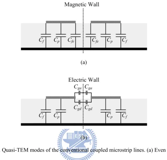
Symmetric coupled microstrip lines, as shown in Fig. 1-2(a), can be analyzed by the even-odd mode analysis. For the even-mode excitation, the normal component of the electric field at the symmetry plane is zero, which leads to a magnetic wall. For the odd-mode excitation, the symmetry plane behaves like an electric wall. Fig. 2-10 shows the capacitance representation for the even- and odd-mode excitations. The even- and odd-mode capacitances (Ce, Co) for either of the coupled lines are given by
e p f fe
C =C +C +C (2.36)
o p f gd ga
25
where Cp is a parallel-plate capacitance per unit length between the signal and ground planes. Cf is the fringe capacitance per unit length from the edge of an uncoupled microstrip line, and Cfe is the fringe capacitance per unit length due to the presence of another line. Cga and Cgd are the fringe capacitances per unit length across the coupling gap in the air and dielectric regions, respectively.
The even- and odd-mode effective dielectric constants εre and εro are determined as
e re ae C C ε = (2.38) o ro ao C C ε = (2.39)
where Cae and Cao are the even- and odd-mode capacitances of either of the coupled lines with air as a dielectric substrate. For the coupled microstrip lines, the even-mode electric field distributions are much more concentrated in a dielectric substrate compared to the odd-mode electric field distributions. Consequently, the value of (2.38) is larger than that of (2.39), which means that the even-mode phase velocity is smaller than the odd-mode phase velocity. This will influence the directivity and isolation of the microstrip directional coupler. The even- and odd-mode impedances Z0e and Z0o are given as follows:
0 1 e ae e Z c C C = (2.40) 0 1 o ao o Z c C C = (2.41)
26
2.3.3 Coupled Line Coupler
Fig. 2-11. Single-section microstrip coupled line coupler.
Fig. 2-12. Equivalent circuit for the even-odd mode analysis.
A single-section microstrip coupled line coupler with a coupling length L is depicted in Fig. 2-11. With the definitions of the even- and odd-mode impedances described above, the design equations for the coupler can be obtained by applying the even-odd mode analysis. The equivalent circuit for the even- and odd-mode excitations is shown in Fig. 2-12. For simplicity, assume that the coupler has a terminated impedance Z0, and the even and odd modes of the
coupled lines have the same velocity of propagation (i.e., βe=βo = ). Therefore, the ABCD β matrices for the even and odd modes are given by
0 0 cos sin sin cos e e e e e e jZ A B j C D Z θ θ θ θ ⎡ ⎤ ⎡ ⎤ ⎢ ⎥ = ⎢ ⎥ ⎢ ⎥ ⎣ ⎦ ⎢ ⎥ ⎣ ⎦ (2.42)
27 0 0 cos sin sin cos o o o o o o jZ A B j C D Z θ θ θ θ ⎡ ⎤ ⎡ ⎤ ⎢ ⎥ = ⎢ ⎥ ⎢ ⎥ ⎣ ⎦ ⎢ ⎥ ⎣ ⎦ (2.43)
where θ β= eL=βoL=βL. As a result, the even- and odd-mode reflection coefficients can be obtained as follows: 0 0 0 0 11 33 0 0 0 0 ( )sin 2cos ( )sin e e e e e e Z Z j Z Z S S Z Z j Z Z θ θ θ − = = + + (2.44) 0 0 0 0 11 33 0 0 0 0 ( )sin 2cos ( )sin o o o o o o Z Z j Z Z S S Z Z j Z Z θ θ θ − = = + + . (2.45)
The even- and odd-mode transmission coefficients are calculated as
31 13 0 0 0 0 2 2cos ( )sin e e e e S S Z Z j Z Z θ θ = = + + (2.46) 31 13 0 0 0 0 2 2cos ( )sin o o o o S S Z Z j Z Z θ θ = = + + . (2.47) Since 11 11 11 2 e o S S S = + (2.48) 33 33 33 2 e o S S S = + , (2.49)
28
2
0e 0o 0
Z Z =Z . (2.50)
Thus, the scattering parameters for the single-section coupler can be obtained as follows:
11 22 33 44 0 S =S =S =S = (2.51) 31 31 14 41 23 32 0 2 e o S S S =S =S =S = − = (2.52) 0 0 11 11 0 0 12 21 34 43 0 0 0 0 ( )sin 2 2cos ( )sin e o e o e o Z Z j S S Z Z S S S S Z Z j Z Z θ θ θ − − = = = = = + + (2.53) 31 31 13 31 24 42 0 0 0 0 2 2 2cos ( )sin e o e o S S S S S S Z Z j Z Z θ θ + = = = = = + + . (2.54)
Now we define the coupling factor C as
0 0 0 0 e o e o Z Z C Z Z − = + (2.55)
so that (2.53) and (2.54) become
21 2 sin 1 cos sin jC S C j θ θ θ = − + (2.56) 2 31 2 1 1 cos sin C S C θ j θ − = − + . (2.57)
For the coupler with L=λ/ 4 (i.e., θ π= / 2) and port 1 excitation, the coupling amount to port 2 is at its maximum. Under this condition, the scattering matrix is
29 2 2 2 2 0 1 0 0 0 1 [ ] 1 0 0 0 1 0 C j C C j C S j C C j C C ⎡ − − ⎤ ⎢ ⎥ ⎢ − − ⎥ = ⎢ ⎥ ⎢− − ⎥ ⎢ ⎥ ⎢ − − ⎥ ⎣ ⎦ . (2.58)
As a result, the maximum value of coupling is C for the coupled line coupler. The design equations for the even- and odd-mode impedances and the coupling factor are given by
0 0 1 1 e C Z Z C + = − (2.59) 0 0 1 1 o C Z Z C − = + . (2.60)
Thus, the coupling strength of the microstrip coupled line coupler can be determined by the even- and odd-mode impedances. Furthermore, the stronger the coupling is, the larger the difference between the even- and odd-mode impedances is. This implies the narrow line width and gap spacing.
The coupling, directivity, and isolation are the three quantities to characterize a directional coupler and are defined as follows:
1 2 21 1 (dB) 10log 20log | | P Coupling P S = = (2.61) 2 21 4 41 | | (dB) 10log 20log | | P S Directivity P S = = (2.62) 1 4 41 1 (dB) 10log 20log | | P Isolation P S = = (2.63)
where P1 is the power incident at port 1, and P2 and P4 are the power outputs at ports 2 and 4,
respectively.
30
Fig. 2-13. N-section symmetric multisection coupled line coupler.
multisection coupled line coupler is required to increase the bandwidth. A multisection coupled line coupler can be either symmetric or asymmetric depending on whether it has end-to-end symmetry. In this dissertation, we design a symmetric multisection coupled line coupler which has an odd number of coupling sections, as depicted in Fig. 2-13. For a multi- section coupled line coupler, each coupling section is a quarter-wavelength long at the center frequency and is specified by the even- and odd-mode impedances [58]. The even- and odd-mode impedances for each coupling section have been tabulated in [59].
31
Chapter 3 N
OVEL
L
OW-
I
MPEDANCE
M
ICROSTRIP
L
INE
FOR
Q
UARTER-
W
AVELENGTH
S
TEPPED-
I
MPEDANCE
R
ESONATOR
F
ILTERS
In this chapter, a new low-impedance microstrip line is proposed and applied in the conventional microstrip quarter-wavelength stepped-impedance resonator (SIR). The pro- posed microstrip line has the signal and ground strips on the same plane to provide another degree of freedom to control the characteristic impedance. The experimental filters have compact sizes, high selectivity, and wide stopband range. More importantly, it can be used to decrease the sensitivity of the SIR to fabrication tolerances.
3.1 Fabrication-Tolerant Microstrip Quarter-Wavelength SIR
Filter
The etching error causes the serious resonant frequency drift of a microstrip SIR. Fig. 3-1(a) depicts the fabrication tolerance in the conventional λ/4 microstrip SIR (i.e., ∆WU for under-etching and ∆WO for over-etching). The normalized resonant frequency versus the percentage variation of the impedance ratio R is shown in Fig. 3-1(b), where different curves correspond to different amounts of variation in R due to etching errors. It is observed that small changes in the impedance ratio would contribute to obvious variations in the resonant frequency. As an example, consider two conventional λ/4 microstrip SIRs, as shown in Fig. 3-1(a), with different physical dimensions on the substrate with a dielectric constant of 3.6 and a thickness of 0.5 mm. The first case is WH =0.225 mm and WL =3.45 mm, which
corresponds to R=0.204. The second case is WH =1.25 mm and WL =1.45 mm, which corresponds to R=0.906. For ΔWO =0.025 mm (i.e., over-etching 0.05 mm), the im-