國 立 交 通 大 學
電信工程研究所
碩 士 論 文
可抑制後波瓣的單一導體帶狀天線之設計
A Technique for Back Lobe Suppression of
Single-Conductor Strip Antenna
研究生:林學群
(Hsueh-Chun Lin)
指導教授:周復芳 博士
(Dr. Christina F. Jou)
可抑制後波瓣的單一導體帶狀天線之設計
A Technique for Back Lobe Suppression of
Single-Conductor Strip Antenna
研 究 生:林學群 Student : Hsueh-Chun Lin
指導教授:周復芳博士 Advisor : Dr. Christina F. Jou
國 立 交 通 大 學 電信工程研究所
碩 士 論 文
A Thesis
Submitted to Institute of Communication Engineering College of Electrical Engineering and Computer Science
National Chiao Tung University in Partial Fulfillment of the Requirements
for the Degree of Master of Science in communication Engineering
June 2013
Hsinchu, Taiwan, Republic of China
i
可抑制後波瓣的單一導體帶狀天線之設計
研究生:林學群 指導教授:周復芳 博士 國立交通大學 電信工程研究所 中文摘要 在本論文中,首先介紹了漏波的條件,接著在理論上採用全波分析法-頻域法 (spectral domain approach)得到單一導體結構的第一高階洩漏模的傳播常數,其中在空間 波輻射頻段,正規化的相位常數非常接近 1,透過洩漏波天線洩漏角度之關係式可得知 此天線之主波束(main beam)幾乎固定在端射(end-fire)方向。由於單一導體結構的第一高 階洩漏模的基本物理特性為完美電牆(perfect electric wall)中心對稱,表示縱向電流為奇 對稱分布而橫向電流為偶對稱分布,所以我們使用平衡式微帶線和反向平衡式微帶線來 饋入以激發此模態,並成功地設計出具有高增益與寬頻的單一導體帶狀洩漏波天線。 從此天線的輻射場型圖(radiation pattern)之模擬結果,我們觀察到後波瓣(back lobe) 的輻射相當大。在分析了單一導體帶狀洩漏波天線的結構之後,我們推斷出饋入電路中 的訊號回流機制會造成向天線左右兩端以及後端的輻射。為了抑制這種現象,我們利用 兩個寬頻巴倫(balun)以上下顛倒的方式分別接在饋入電路的左右兩側,而實驗的結果也 證實天線的前後輻射比(front-to-back ratio)確實有了明顯的改善(此一構想是將回流路徑 中的訊號當作巴倫的輸入訊號,而在兩輸出端可產生大小相同、相位差卻為180的反相 訊號,最後將其匯合後來達到抵消的效果,因此向後端福射的效應也隨之減小)。ii
A Technique for Back Lobe Suppression of
Single-Conductor Strip Antenna
Student: Hsueh-Chun Lin Advisor: Dr. Christina F. Jou
Institute of Communications Engineering National Chiao Tung University
Abstract
This thesis presents the condition of leakage and mode distinction at first; then the well-known full-wave method, spectral domain approach, is applied to investigate the propagation characteristics of the first higher-order mode of the single-conductor strip structure. In this case, the normalized phase constant is very close to 1 in the space-wave leaky region. By the leakage angle equation of leaky-wave antenna, we find that the main beam of this antenna is fixed in the end-fire direction over a broadband region. For the first higher-order leaky mode in this structure, a virtual perfect electric wall is assumed at the center of the strip, this means that the longitudinal currents are odd-symmetric and the transverse currents are even-symmetric with respect to the center. A broadband planar feeding structure based on the balanced microstrip lines and the inverted balanced microstrip lines is developed to feed this single-conductor strip structure and thus excite the first higher-order leaky mode. Then, a high gain and wideband leaky-wave antenna is implemented.
From the radiation patterns of our single-conductor strip leaky-wave antenna, we observe that the back lobe is quite large. After analyzing the single-conductor strip leaky-wave antenna, we conclude that the feeding structure of this antenna causes this undesired effect. In
iii
order to alleviate this undesired radiation from the feeding structure, we turn two broadband planar baluns upside down and attach themselves to the left and right sides of the feeding structure, respectively. Experimental results show significant improvement of the front-to-back ratio of this antenna.
iv
誌謝
本論文的完成首先要感謝我的指導教授 周復芳博士,在研究所的求學過程中,提 供我一個優良的學習環境,並且當我在研究上遇到瓶頸時,總是能夠適時地給予鼓勵和 經驗上的分享,使我得而在兩年內完成碩士研究。同時也要非常感謝 林育德教授,無 論在參考文獻上的推薦,或者在數學推導以及數值處理技巧上給我的指導與建議,讓我 在微波及天線的領域得到相當多的知識與訓練。再者感謝吳霖堃教授、王健仁教授在口 試的時候前來指導,由於他們的寶貴意見才使得本論文更臻完整。特別感謝吳霖堃教授 在課餘時間仍不厭其煩地解答我修課上的任何問題。 接著要感謝的是已經畢業的學長奇哲,在研究上提供了很重要的靈感,並且耐心地 教會我操作遠場量測室。也感謝奕心在修課時我們時常能互相幫助對方,也會一起討論 各自的研究主題。當然還要感謝 925 實驗室的助理薔芸總是在我低潮的時候跳出來幫我 打氣,也在實驗室扮演了保姆的角色照顧大家。和你們在碩一相處的這段日子才使得碩 士生活變得更加多采多姿。也謝謝學弟昱升、育杰能夠適時地分擔實驗室的工作,讓我 能更專心於研究上。 感謝超舜學長、玠瑝學長、政皓學長,無論是在學業上或是生活上給予我的指導與 關心。感謝最常和我一起相互砥礪,一起度過許多困難的玠倫。感謝常陪我聊天和運動 的學弟政緯。也感謝在 919 實驗室裡一起同甘共苦的各位,因為有你們,在這實驗室裡 總是充滿著歡笑,讓我在面對研究壓力之餘,能夠感受到我們是一起奮鬥的夥伴,也讓 我更有信心去面對接下來的挑戰。 感謝宜哲學長、正元學長以及科文、則宇等同學在課業和研究上的幫助。還有感謝 時常有交集的 916、917 和 923 實驗室的各位學長、同學或學弟,謝謝你們在辦活動的 時候總是會算我一份。也謝謝海睿、烜瑋、群明、子峻、觀文、佳龍、立維,你們是我 在召喚峽谷上的好戰友。 最後要感謝最支持我的家人,我最親愛的爸爸、媽媽還有兩個姊姊,謝謝你們無條 件的支持,讓我沒有後顧之憂地完成學業。v
Contents
中文摘要 ……….………..…..I Abstract.………..……...………… II 誌謝.………..……...……… IV Contents.………..……...………...VList of Figures.………..……...……..VII
List of Tables.………..……...………XIII
Chapter 1 Introduction ... 1
1.1 Motivation ... 1
1.2 Organization of This Thesis ... 2
Chapter 2 Physical Properties of Leaky Waves ... 3
2.1 Leakage Condition ... 3
2.1.1 Surface-Wave Leaky Mode ... 3
2.1.2 Space-Wave Leaky Mode ... 7
2.2 Mode Distinction ... 8
Chapter 3 Analysis and Numerical Results ... 10
3.1 Space Domain to Spectral Domain ... 10
3.2 SDA on Single-Conductor Strip Structure ... 12
3.2.1 Field Approach ... 12
3.2.2 Choice of Basis Functions ... 17
3.2.3 Method of Solution ... 19
3.2.4 Discussion of Integration Contours ... 21
vi
Chapter 4 Antenna Design, Simulation and Measurement ... 28
4.1 Design of Single-Conductor Strip Leaky-Wave Antenna ... 28
4.1.1 Broadband Planar Feeding Structure ... 28
4.1.2 Performance of Single-Conductor Strip Leaky-Wave Antenna ... 35
4.2 Reduction of the Back Lobe ... 44
4.2.1 Consideration during Design Procedure ... 44
4.2.2 Broadband Planar Balun ... 46
4.2.3 Comparison of Simulated Results Between Original and Modified Single-Conductor Strip Leaky-Wave Antenna ... 49
4.2.4 Fabrication and Measurement of Modified Single-Conductor Strip Leaky-Wave Antenna... 55
Chapter 5 Conclusion and Future Work ... 62
5.1 Conclusion ... 62 5.2 Future Work ... 62 References ……….63 Appendix A ... 65 Appendix B ... 69 Appendix C ... 73 Appendix D ... 74 Appendix E ... 83
vii
List of Figures
Fig. 2.1 Coplanar waveguide structure. ... 4
Fig. 2.2 Top view of a metal strip lying on the substrate, showing the angle of leakage into the surface wave on the surrounding substrate. ... 4
Fig. 2.3 A typical dispersion plot for a CPW. For the mode becomes leaky, in accordance with Eq. (2.3). ... 5
Fig. 2.4 Conductor-backed coplanar waveguide structure. ... 6
Fig. 2.5 Dispersion curves of the normalized phase constant of the surface-wave leaky mode for a CBCPW. ... 6
Fig. 2.6 Conductor-backed slotline structure. ... 6
Fig. 2.7 The amplitude decays in the z direction ( ) due to leakage loss, but in the x direction at a given z, the amplitude increases exponentially ( ). ... 6
Fig. 2.8 Microstrip line structure. ... 7
Fig. 2.9 Cross section of a microstrip line. ... 7
Fig. 2.10 Radiation leakage in a microstrip line at the air-substrate interface. ... 8
Fig. 2.11 Behavior of the normalized phase constant and the attenuation constant as a function of frequency for the first higher-order mode of the microstrip line. ... 9
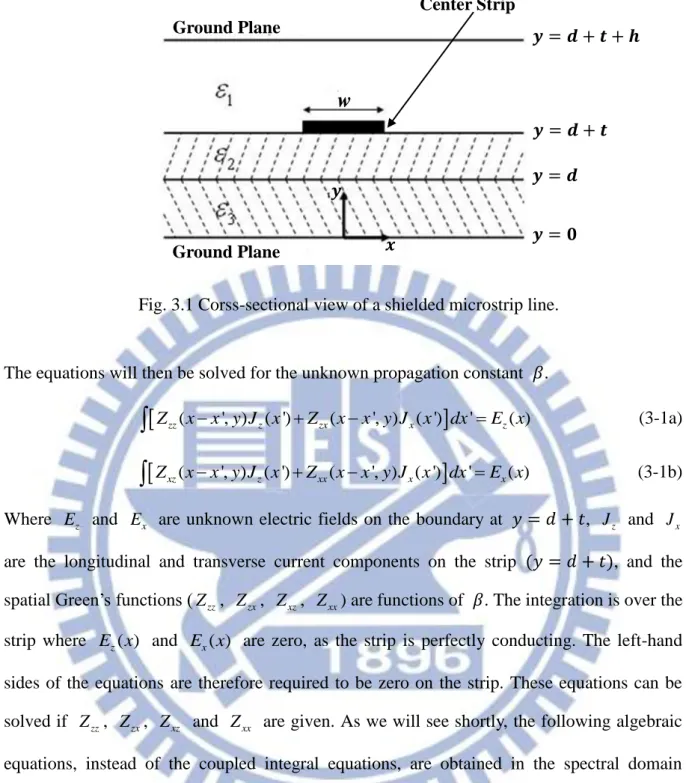
Fig. 3.1 Corss-sectional view of a shielded microstrip line. ... 11
Fig. 3.2(a) Single-conductor strip structure. ... 12
Fig. 3.2(b) Cross-sectional view of a single-conductor strip structure. ... 12 Fig. 3.3 Cross-sectional view of a single-conductor strip structure. A virtual
viii
higher-order mode. ... 17
Fig. 3.4 Shapes of basis functions ... 18
Fig. 3.5 Integral paths of the inverse Fourier transform on the kx plane. ... 22
Fig. 3.6 Integral paths of the inverse Fourier transform on the kx plane. ... 24
Fig. 3.7 Behavior of the normalized phase constants and the normalized attenuation constants as a function of frequencies for the first higher order mode of the single conductor strip structure with and for different strip widths. ... 25
Fig. 3.8 Behavior of the normalized phase constants and the normalized attenuation constants as a function of frequencies for the first higher order mode of the single conductor strip structure with and for different dielectric constants. ………. 26
Fig. 3.9 Behavior of the normalized phase constants and the normalized attenuation constants as a function of frequencies for the first higher order mode of the single conductor strip structure with and for different substrate thicknesses. ………. 27
Fig. 4.1 An appropriate feeding structure which generates two out-of-phase currents is used to feed the single-conductor strip structure and thus excites the first higher order leaky mode. ... 29 Fig. 4.2(a) Diagram of the broadband balun structure used to excite the first higher
order leaky mode of the single-conductor strip line. The strips of the balun on the lower side of the substrate are connected to each other and returned back to the original ground plane of the microstrip line. This feeding structure consists of (I) a conventional microstrip line; (II) a microstrip-to-balanced-microstrip-line transition; (III) a
ix
the balanced microstrip lines is changed to form the inverted balanced
microstrip lines. ... 30
Fig. 4.2(c) The strip of the balun on the lower side of the substrate. ... 30
Fig. 4.2(b) The strip of the balun on the upper side of the substrate. ... 30
Fig. 4.3(a) Gradually tapering the ground plane to a width equal to the strip width w makes conventional microstrip line a balanced microstrip line. ... 31
Fig. 4.3(b) Cross-sectional view of a balanced microstrip line, with a strip of positive voltage on the upper side of the substrate and a strip of negative voltage on the lower side of the substrate. ... 31
Fig. 4.4(a) Top view of the inverted balanced microstrip line. ... 32
Fig. 4.4(b) The width of the bent stubs: ; the length of the bent stubs: and ; the gap width: ; the diameter of vias: ; the slanted angle is 45 degrees. .... 33
Fig. 4.4(c) Signal flow graph of the inverted balanced microstrip line. ... 33
Fig. 4.5 Two pairs of the broadband planar baluns on the upper and lower substrate sides, respectively. ... 34
Fig. 4.6 Geometry of the single-conductor strip leaky-wave antenna. ... 35
Fig. 4.7(a) Side view of the broadband planar feeding structure. ... 36
Fig. 4.7(b) Top view of the broadband planar feeding structure. ... 36
Fig. 4.8(a) Simulated S-parameter magnitudes of the broadband planar feeding structure. ... 37
Fig. 4.8(b) Simulated phase difference of the broadband planar feeding structure. .. 37
Fig. 4.9 Normalized propagation constant of the single-conductor strip structure with a strip width of w32.5mm, a dielectric constant of r 3.55, and a thickness of h0.508mm. ... 38 Fig. 4.10 Simulated return loss of the single-conductor strip leaky-wave antenna. 39
x
Fig. 4.11(a) Simulated E-plane (x-y plane) radiation pattern of the single-conductor
strip leaky-wave antenna with a gain of 6.24 dBi at 5.2 GHz. ... 40
Fig. 4.11(b) Simulated H-plane (y-z plane) radiation pattern of the single-conductor strip leaky-wave antenna at 5.2 GHz. ... 40
Fig. 4.11(c) Simulated E-plane (x-y plane) radiation pattern of the single-conductor strip leaky-wave antenna with a gain of 6.96 dBi at 5.4 GHz. ... 41
Fig. 4.11(d) Simulated H-plane (y-z plane) radiation pattern of the single-conductor strip leaky-wave antenna at 5.4 GHz. ... 41
Fig. 4.11(e) Simulated E-plane (x-y plane) radiation pattern of the single-conductor strip leaky-wave antenna with a gain of 7.23 dBi at 5.6 GHz. ... 42
Fig. 4.11(f) Simulated H-plane (y-z plane) radiation pattern of the single-conductor strip leaky-wave antenna at 5.6 GHz. ... 42
Fig. 4.11(g) Simulated E-plane (x-y plane) radiation pattern of the single-conductor strip leaky-wave antenna with a gain of 7.51 dBi at 5.8 GHz. ... 43
Fig. 4.11(h) Simulated H-plane (y-z plane) radiation pattern of the single-conductor strip leaky-wave antenna at 5.8 GHz. ... 43
Fig. 4.12 Surface current in the current returning paths in the ground plane. ... 44
Fig. 4.13(a) Top view of the modified single-conductor strip leaky-wave antenna. ... 45
Fig. 4.13(b) Back view of the modified single-conductor strip leaky-wave antenna. . 45
Fig. 4.14(a) Two microstrip-to-slotline transitions connected back-to-back for 180 phase change and (b) mechanism for 180 phase change... 46
Fig. 4.15(a) Top view of the broadband planar balun. ... 47
Fig. 4.15(b) Back view of the broadband planar balun. ... 47
Fig. 4.16(a) Simulated S-parameter magnitudes of the broadband planar balun. ... 48
Fig. 4.16(b) Simulated phase difference of the broadband planar balun. ... 48 Fig. 4.17 Comparison of the simulated surfaces current in the current returning
xi
paths in the ground plane between the original and the modified
single-conductor strip leaky-wave antenna. ………...……….49 Fig. 4.18(a) Comparison of the simulated E-plane (x-y plane) radiation patterns
between the original and the modified single-conductor strip leaky-wave antenna at 5.2 GHz. ... 50 Fig. 4.18(b) Comparison of the simulated E-plane (x-y plane) radiation patterns
between the original and the modified single-conductor strip leaky-wave antenna at 5.3 GHz. ... 50 Fig. 4.18(c) Comparison of the simulated E-plane (x-y plane) radiation patterns
between the original and the modified single-conductor strip leaky-wave antenna at 5.4 GHz. ... 51 Fig. 4.18(d) Comparison of the simulated E-plane (x-y plane) radiation patterns
between the original and the modified single-conductor strip leaky-wave antenna at 5.5 GHz. ... 51 Fig. 4.18(e) Comparison of the simulated E-plane (x-y plane) radiation patterns
between the original and the modified single-conductor strip leaky-wave antenna at 5.6 GHz. ... 52 Fig. 4.18(f) Comparison of the simulated E-plane (x-y plane) radiation patterns
between the original and the modified single-conductor strip leaky-wave antenna at 5.7 GHz. ... 52 Fig. 4.18(g) Comparison of the simulated E-plane (x-y plane) radiation patterns
between the original and the modified single-conductor strip leaky-wave antenna at 5.8 GHz. ... 53 Fig. 4.19 Comparison of the simulated front-to-back ratio between the original and the modified single-conductor strip leaky-wave antenna. ... 54 Fig. 4.20(a) Top view of the fabricated modified single-conductor strip leaky-wave
xii
antenna. ... 55 Fig. 4.20(b) Back view of the fabricated modified single-conductor strip leaky-wave
antenna. ... 55 Fig. 4.21 Meauured and simulated return loss of the modified single-conductor
strip leaky-wave antenna. ... 56 Fig. 4.22(a) Meauured and simulated E-plane (x-y plane) radiation patterns of the
modified single-conductor strip leaky-wave antenna at 5.2 GHz. ... 57 Fig. 4.22(b) Meauured and simulated E-plane (x-y plane) radiation patterns of the
modified single-conductor strip leaky-wave antenna at 5.3 GHz. ... 57 Fig. 4.22(c) Meauured and simulated E-plane (x-y plane) radiation patterns of the
modified single-conductor strip leaky-wave antenna at 5.4 GHz. ... 58 Fig. 4.22(d) Meauured and simulated E-plane (x-y plane) radiation patterns of the
modified single-conductor strip leaky-wave antenna at 5.5 GHz. ... 58 Fig. 4.22(e) Meauured and simulated E-plane (x-y plane) radiation patterns of the
modified single-conductor strip leaky-wave antenna at 5.6 GHz. ... 59 Fig. 4.22(f) Meauured and simulated E-plane (x-y plane) radiation patterns of the
modified single-conductor strip leaky-wave antenna at 5.7 GHz. ... 59 Fig. 4.22(g) Meauured and simulated E-plane (x-y plane) radiation patterns of the
modified single-conductor strip leaky-wave antenna at 5.8 GHz. ... 60 Fig. 4.23 Comparison of the measured and simulated front-to-back ratio of the
xiii
List of Tables
Table 4.1 Simulated gain and the back lobe of the original and the modified
single-conductor strip leaky-wave antenna ... 53 Table 4.2 Simulated front-to-back ratio of the original and the modified
single-conductor strip leaky-wave antenna ... 54 Table 4.3 Measured and simulated results of the gain and the back lobe of the
modified single-conductor strip leaky-wave antenna ... 60 Table 4.4 Measured and simulated front-to-back ratio of the modified
1
Chapter 1
Introduction
1.1 MOTIVATION
The printed-circuit type antenna is the best choice for the trend in antenna development, which is compact, relatively inexpensive, and highly reliable. In RF and narrow-band applications, resonant type antennas are most widely used since the matching network design is simple, and the antenna size is small when using a higher dielectric constant substrate. However, in millimeter wave and wide band applications, the resonant type antenna (usually a patch one) is no longer the best choice due to its inherent nature such as a narrow operational bandwidth, complexity in matching network design for array applications, and serious tolerance requirement in fabrication. So the printed circuit type leaky wave antenna is a better candidate in millimeter wave applications owing to its advantages such as simplicity in array design, broad band, beam-scanning capability, and relaxed requirement of tolerance.
In [1], experimental verification of a microstrip-line higher order mode leaky-wave antenna was conducted without explaining the physics underlying the design of the antenna. In [2], [3], Oliner explained the physics underlying the leaky-wave antenna design constructed in [1], and presented analysis data for the antenna design. In [4], [5], the familiar spectral-domain analysis was used, with the appropriate choice of branch cuts and integration contours. Thus, numerous issues about leaky-wave antennas are subsequently investigated, such as full-wave analysis of leaky modes, feeding structures, antenna arrays, etc.
In [6], A leaky-wave broad band antenna that has only a single-conductor strip on a substrate but no ground plane was presented. That absence of a ground plane allows both TE0
2
feature of the single-conductor strip leaky-wave antenna is that the main beam is fixed in the end-fire direction over a broad band region. This pattern feature is useful in some applications that require a main beam in the end-fire direction. From the radiation patterns of this leaky-wave antenna, we observe that the back lobe is quite large. In this thesis, a novel method is proposed to alleviate this undesired radiation.
1.2 ORGANIZATION OF THIS THESIS
This thesis is divided into four parts. In chapter 2, we introduce the condition of leakage and mode distinction. In chapter3, the full-wave method, spectral domain approach is used to analyze the propagation characteristics of the first higher-order leaky mode of the single-conductor strip structure. The numerical results are calculated to decide the operating frequency band of leaky-wave antenna. In chapter 4, in order to alleviate the large back lobe of the single-conductor leaky-wave antenna, the feeding structure is modified with two broadband planar baluns. Finally, some conclusions and future work are made in Chapter 5.
3
Chapter 2
Physical Properties of Leaky Waves
Most planar transmission lines used in microwave and millimeter-wave frequency region can exhibit several new propagation phenomena. They have relevance to leaky modes that leak power in the form of the surface wave and/or the space wave. Both the surface wave leakage and the space wave leakage on planar transmission structures can produce unwanted crosstalk between neighboring parts of a circuit and undesired package effects, or can be used to create new circuit components and antennas. In this chapter, we will explain when leakage can occur.
2.1 LEAKAGE CONDITION
In general, leaky modes can be divided in two types: surface-wave leaky modes and space-wave leaky modes [3]. The surface-wave leaky modes are those modes that leak power in the form of surface waves on the surrounding substrate as they propagate. The space-wave leaky modes leak power in the form of space waves radiating into space as well as surface waves.
2.1.1 Surface-Wave Leaky Mode
Fig. 2.1 illustrates the structure of a coplanar waveguide (CPW). As shown in Fig. 2.2, the surface wave leakage condition can be examined from the top view of a metal strip lying on the air-substrate interface, where this strip can represent the center strip of CPW, or the strip of microstrip line, or whatever. From the figure the relation below is observed
(2-1) where is the phase constant of the dominant mode guided along the z-direction, is the
4
transverse wavenumber, and is the propagation wavenumber of the surface wave supported on the substrate in the vicinity of the guiding strip. If , Eq. (2.1) results in , then is seen to be imaginary, it means that the modal field decays transversely in
the x-direction and the mode guided in the z-direction is purely bound. On the other hand, if , Eq. (2.1) results in , then is seen to be real, it means that power will leak from the guided mode at an angle in the form of surface waves on the surrounding substrate, or a parallel-plate mode if there exists a top cover above the substrate. The angle can be defined by
(2-2) where is the free space wavenumber. For this reason, the surface wave leakage occurs when the condition is satisfied, or, dividing both sides by , that can be written as
(2-3)
Truly, when leakage occurs, the wavenumber of the guided mode becomes complex ,
where is the attenuation constant. Eq. (2.2) is no longer exactly correct, but it is still a
Fig. 2.2 Top view of a metal strip lying on the substrate, showing the angle of leakage into the surface wave on the surrounding substrate.
Fig. 2.1 Coplanar waveguide structure.
5
good approximation.
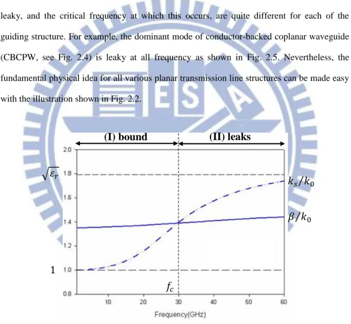
We observe from the dispersion curves for a CPW in Fig. 2.3 that Eq. (2.3) is satisfied when frequency f is greater than the critical frequency at which the two curves cross in Fig. 2.3 [7]. All of the uniplanar lines will leak power above some critical frequency. The power will radiate away in the lateral direction at an angle that varies with frequency, and the leakage rate is also frequency-sensitive. The manner in which the dominant mode becomes leaky, and the critical frequency at which this occurs, are quite different for each of the guiding structure. For example, the dominant mode of conductor-backed coplanar waveguide (CBCPW, see Fig. 2.4) is leaky at all frequency as shown in Fig. 2.5. Nevertheless, the fundamental physical idea for all various planar transmission line structures can be made easy with the illustration shown in Fig. 2.2.
(II) leaks
(I) bound
Fig. 2.3 A typical dispersion plot for a CPW. For the mode becomes leaky, in accordance with Eq. (2.3).
6
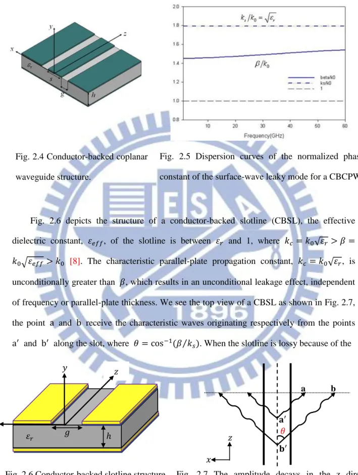
Fig. 2.6 depicts the structure of a conductor-backed slotline (CBSL), the effective dielectric constant, , of the slotline is between and 1, where
[8]. The characteristic parallel-plate propagation constant, , is
unconditionally greater than , which results in an unconditional leakage effect, independent of frequency or parallel-plate thickness. We see the top view of a CBSL as shown in Fig. 2.7, the point and receive the characteristic waves originating respectively from the points and along the slot, where . When the slotline is lossy because of the
Fig. 2.5 Dispersion curves of the normalized phase constant of the surface-wave leaky mode for a CBCPW.
Fig. 2.4 Conductor-backed coplanar waveguide structure.
b a
Fig. 2.6 Conductor-backed slotline structure.
Fig. 2.7 The amplitude decays in the z direction ( ) due to leakage loss, but in the x direction at a given z, the amplitude increases exponentially ( ).
7
leakage effect, the electric field on the slotline has an exponential decay along the propagation direction, resulting in a larger value at than at . Hence, the field magnitude at b tends to be larger than that at a, which explains an increasing trend of the electric field in the transverse direction.
2.1.2 Space-Wave Leaky Mode
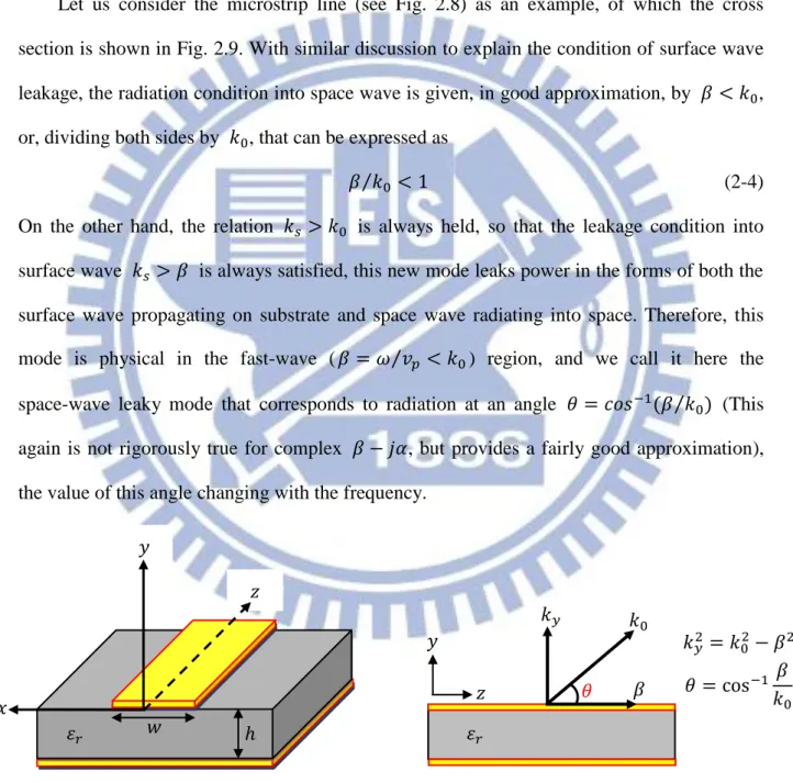
Let us consider the microstrip line (see Fig. 2.8) as an example, of which the cross section is shown in Fig. 2.9. With similar discussion to explain the condition of surface wave leakage, the radiation condition into space wave is given, in good approximation, by , or, dividing both sides by , that can be expressed as
(2-4) On the other hand, the relation is always held, so that the leakage condition into surface wave is always satisfied, this new mode leaks power in the forms of both the surface wave propagating on substrate and space wave radiating into space. Therefore, this mode is physical in the fast-wave ( ) region, and we call it here the space-wave leaky mode that corresponds to radiation at an angle (This again is not rigorously true for complex , but provides a fairly good approximation), the value of this angle changing with the frequency.
Fig. 2.8 Microstrip line structure. Fig. 2.9 Cross section of a microstrip line.
8
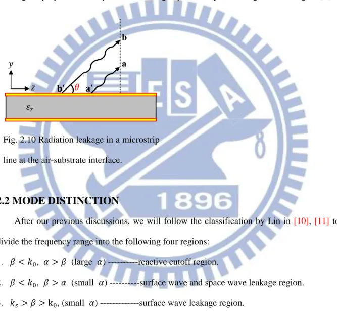
Also, with similar discussion to explain the exponential growth of the electric field in the transverse direction for the surface wave leakage case, one can explain in this case a nondecaying field in the normal direction ( ) (see Fig. 2.10) for the space wave leakage. Interestingly, any forward wave that decays in the longitudinal direction due to leakage loss must increase exponentially in the surrounding air region. The leaky wave is often described as being "improper" or "nonspectral", meaning exponentially increasing in the air region [9].
2.2 MODE DISTINCTION
After our previous discussions, we will follow the classification by Lin in [10], [11] to divide the frequency range into the following four regions:
1. , (large ) ---reactive cutoff region.
2. , (small ) ---surface wave and space wave leakage region. 3. , (small ) ---surface wave leakage region.
4. , ---bound mode region.
In the radiation region ( ) with a larger attenuation constant is reactive and below cutoff, and has a different mode nature from that with a smaller attenuation constant. Therefore, this radiation-frequency region can further be divided into two regions with decreasing frequency: the antenna-mode region ( , ) where most of the guided power leaks away in the
b a
Fig. 2.10 Radiation leakage in a microstrip line at the air-substrate interface.
9
forms of space wave and surface wave, and the reactive cutoff region, where most of the power is reflected back to the feed line, however, the propagation constant is still a complex number with a small real part, , and a large imaginary part, , indicating that the mode is not strictly cutoff, but a very small portion of energy still propagates down the transmission line. In design of leaky-wave antennas, this distinction of mode nature in the radiation region is essential since the antenna efficiency is low in the reactive-mode region. We can simply define the lower frequency edge ( ) and the upper frequency edge ( ) of the usable frequency range for the leaky wave antenna:
(2-5) (2-6) Fig. 2.11 shows the normalized propagation constant for the first higher-order mode of microstrip line as an example. For this case ( , , ), the usable frequency range for the leaky wave antenna is approximately 5.1 to 6.1 GHz.
Fig. 2.11 Behavior of the normalized phase constant and the attenuation constant as a function of frequency for the first higher-order mode of the microstrip line.
10
Chapter 3
Analysis and Numerical Results
Planar transmission line analysis in the Fourier transform domain (or spectral domain) is superior to many numerical methods in the spatial domain. The spectral domain approach (SDA) was presented by Itoh and Mittra [12], this method is basically a modification of Galerkin’s approach adapted for application in the Fourier transform domain, or spectral domain (In SDA, Galerkin’s method is used to yield a homogeneous system of equations to determine the propagation constant). The Fourier transform is taken along the direction parallel to the substrate and perpendicular to the strip. The main reason the SDA is numerically efficient is that it requires a significant analytical preprocessing. This feature in turn imposes a certain restriction on the applicability of the method. One of the limitations is that SDA requires infinitesimal thickness for the strip conductor. It is also difficult to treat the structure with a strip having finite conductivity. No discontinuity in the substrate in the sideward direction is allowed. In spite of these limitations, however, SDA is one of the most popular and widely used numerical techniques.
In this chapter, the general approach (field approach) is described [13].
3.1 SPACE DOMAIN TO SPECTRAL DOMAIN
Before the detailed formulation process is presented, let us compare the types of equations obtained by the SDA and those obtained by a typical space domain formulation [13]. Fig. 3.1 shows a shielded microstrip line with its cross-sectional view as an example. In conventional space domain analysis, the structure can be analyzed by first formulating the following coupled homogeneous integral equations.
11
The equations will then be solved for the unknown propagation constant .
Zzz(xx y J x', ) z( ')Zzx(xx y J x', ) x( ')
dx'E xz( )
(3-1a)
Zxz(xx y J x', ) z( ')Zxx(xx y J x', ) x( ')
dx'E xx( )
(3-1b)Where Ez and Ex are unknown electric fields on the boundary at , Jz and Jx
are the longitudinal and transverse current components on the strip , and the spatial Green’s functions (Zzz, Zzx, Zxz, Zxx) are functions of . The integration is over the strip where E xz( ) and E xx( ) are zero, as the strip is perfectly conducting. The left-hand sides of the equations are therefore required to be zero on the strip. These equations can be solved if Zzz, Zzx, Zxz and Zxx are given. As we will see shortly, the following algebraic equations, instead of the coupled integral equations, are obtained in the spectral domain formulation. These equations are Fourier transforms of the coupled integral equations.
( , ) ( ) ( , ) ( ) ( , ) zz x z x zx x x x z x Z k dt J k Z k dt J k E k dt (3-2a) ( , ) ( ) ( , ) ( ) ( , ) xz x z x xx x x x x x Z k dt J k Z k dt J k E k dt (3-2b) Where quantities with tildes (~) are Fourier transforms of corresponding quantities.
Ground Plane Center Strip
w
Fig. 3.1 Corss-sectional view of a shielded microstrip line.
12
The Fourier and inverse Fourier transform are defined as
( ) ( ) jk xx x k x e dx
(3-3a) ( ) 1 ( ) 2π x jk x x x x k e dk
(3-3b)The right-hand side of Eqs. (3-2) is no longer zero because the Fourier transform requires integration over all x, not only over the strip. The equations contain four unknowns Jz, Jx,
z
E , Ex with unknown . Ez and Ex, however, will be eliminated in the solution process based on the Galerkin procedure.
3.2 SDA ON SINGLE-CONDUCTOR STRIP STRUCTURE
3.2.1 Field Approach
In this section, the Green’s impedance functions Zzz, Zzx, Zxz, Zxx will be derived
for the single-conductor strip structure in Fig. 3.2. Only one perfect conducting and infinitely thin strip is located at the interface between a semi-infinite air layer and an isotropic lossless substrate, with a dielectric constant of and a thickness of h. This structure is assumed to be uniform and infinite in both x- and z-directions. First, the hybrid fields are expressed in terms of Superposition of TE-to-y and TM-to-y expressions [14] with scalar potentials e and h
as follows:
Fig. 3.2(a) Single-conductor strip structure. Fig. 3.2(b) Cross-sectional view of a single-conductor strip structure.
13 2 2 2 2 2 2 ˆ ˆ 1 1 ˆ ˆ ˆ ˆ e h h e x x x z x z e h y y e h h e z z z x z x k k E j jk H jk j y y z y E k H k y y z y k k E j jk H jk j y y z y (3-4) 2 2 ˆ ˆ y j z j k =
Where is permittivity, is permeability, the time convention is implied, and the z dependence is assumed. Each field quantity in (3-4) is a Fourier transform of a corresponding quantity in the space domain (see Appendix A). The Fourier-transformed Helmholtz equation is expressed as (see Appendix A)
2 2 2 2 2 0 x z k k k y (3-5)
The solution for this homogeneous differential equation is described in the form of
2 2 2 2
1cosh 2sinh , x z
c y c y k k k
(3-6)
with appropriate coefficients and . When the boundary conditions at , and are satisfied, the scalar potentials in each region are given as follows:
Region 1: 1( ) 1( ) 1 1 y h y h e e h h A e A e (3-7) Region 2: 2e es i n h2 e c o s h2 B y C y (3-8) 2h hc o s h2 h s i n h2 B y C y Region 3: 3 3 3 3 y y e e h h D e D e (3-9) where each subscript refers to the corresponding region and A , e A , …, h D are unknown h
14
coefficients. is the propagation constant in the y-direction and may be written as . Solution of (3-7) (3-9) into (3-4) yields the field expressions in the three regions:
1 1 3 3 - ( - ) - ( ) 1 1 2 2 2 2 2 2 3 3
( cosh sinh ) ( cosh sinh )
y h y h e h x x y z e e h h x x y z y y e h x x y z E jk A e jk A e E jk B y C y jk B y C y E jk D e jk D e 1 3 - ( - ) 2 2 1 1 1 1 2 2 2 2 2 2 2 2 2 2 3 3 3 3 1 ( ) ˆ 1 ( )( sinh cosh ) ˆ 1 ( ) ˆ y h e y e e y y e y E k A e y E k B y C y y E k D e y 1 1 3 3 - ( ) - ( - ) 1 1 2 2 2 2 2 2 3 3 +
( cosh sinh ) ( cosh sinh )
(3 10) y h y h e h z z y x e e h h z z y x y y e h z z y x E jk A e jk A e E jk B y C y jk B y C y E jk D e jk D e 1 1 3 3 - ( - ) - ( ) 1 1 2 2 2 2 2 2 3 3
( sinh cosh ) ( sinh cosh )
y h y h e h x z x z e e h h x z x z y y e h x z x z H jk A e jk A e H jk B y C y jk B y C y H jk D e jk D e 1 3 - ( - ) 2 2 1 1 1 1 2 2 2 2 2 2 2 2 2 2 3 3 3 3 1 ( ) ˆ 1 ( )( cosh sinh ) ˆ 1 ( ) ˆ y h h y h h y y h y H k A e z H k B y C y z H k D e z 1 1 3 3 - ( - ) - ( ) 1 1 2 2 2 2 2 2 3 3
( sinh cosh ) ( sinh cosh )
y h y h e h z x z z e e h h z x z z y y e h z x z z H jk A e jk A e H jk B y C y jk B y C y H jk D e jk D e 2= 2 2 2 = 1 , 2 , 3 ˆ ˆ i i i xi zi i yi zi i i k k k i y z
where each subscript refers to the corresponding region. The unknown coefficients A , e
h
A ,…, D are eliminated by imposing the boundary conditions at each interface. The h boundary conditions in the spectral domain are obtained as the Fourier transforms of those in the space domain. In space domain, the boundary conditions are written as follows,
15 At : 1 2 1 2 2 1 2 1 2 0 2 2 0 2 for all for all ( ) ( ) x x z z z x x x z z x w x w x w x w E E x E E x J x H H J x H H At : 2 3 2 3 2 3 2 3 for all for all for all for all x x z z x x z z E E x E E x H H x H H x
where J xx( ) and J xz( ) are the unknown surface current distributions on the strip at . Notice these quantities need to be introduced so that the boundary conditions are specified for the entire range of x. Otherwise; it is not possible to take Fourier transforms. In the spectral domain, the boundary conditions are now given by the following equations.
At : 1 2 1 2 2 1 2 1 ( ) ( ) x x z z x x z x z z x x E E E E H H J k H H J k (3-11) At : 2 3 2 3 3 2 3 2 0 0 x x z z x x z z E E E E H H H H (3-12)
where J kz( )x and J kx( )x are Fourier transforms of unknown surface current components
( )
z
16
Finally, the algebraic equations are derived in matrix from as follows:
1 1 zz zx z z EJ x xz xx x Z Z E J E G J E Z Z J ( 3 - 1 3 ) 2 2 e h 2 2 1 ( Z + Z ) zz z x x z Z k k k k (3-14) e h 2 2(Z Z ) x z zx x z k k Z k k (3-15) xz zx Z Z (3-16) 2 2 e h 2 2 1 ( Z + Z ) xx x z x z Z k k k k (3-17) 0 0 0 coth 2 coth y y e y y y y h Z h (3-18) 0 0 0 1 1 coth 2 coth z z h z z z z h Z h (3-19) 2 2 2 2 2 2 0 kx kz k0, k0 0 0 2 2 2 2 2 2 0 0 , x z r k k k k 0 0 0 y j , 0 y r j , 0 0 0 z j , 0 z j
The derivation of these formulations is detailed in Appendix B. It should be noted that there is one more set of boundary conditions not used up to this stage. In the space domain, it is
0 for 2 at
z x
E E x w yh (3-20) This set of conditions is incorporated in the solution process as we will see below.
17
3.2.2 Choice of Basis Functions
In order to solve (3-13), the unknown Jz and Jx should be expanded by known basis functions Jzm and Jxm 1 1 ( ) ( ) N z m zm x m M x m xm x m J c J k J d J k
(3-21)Where cm and dm are unknown coefficients. These approximations are assumed that Jz
and Jx have known forms, and the only unknowns in their representation are the amplitude coefficients cm and dm. The basis functions must be chosen to correspond to the odd or even symmetry of the currents for the mode of interest. The current is nonzero only on the strip. Therefore, the basis functions Jzm( )kx and Jxm( )kx must also be chosen such that their inverse Fourier transforms are nonzero only on the strip x w 2. The accuracy of the numerical results can be increased by selecting higher values of M and N, but it is relatively low efficiency because of taking more time during numerical computation. It means that the accuracy and efficiency depend on the numbers of basis functions. As shown in Fig. 3.3, due to the structural symmetry, a virtual perfect electric wall is placed at the center of the single
PEC
Fig. 3.3 Cross-sectional view of a single-conductor strip structure. A virtual perfect electric wall is placed at the center of this structure for the first higher-order mode.
18
conductor strip structure for the first higher-order mode, so odd basis functions for Jz and even basis functions for Jx are chosen [6]. Here, the following set of basis functions is employed [13]:
2 sin (2 1) / ( ) , 1, 2, ..., 1 (2 / ) zm m x w J x m N x w (3-22)
2 cos (2 1) / ( ) , 1, 2, ..., 1 (2 / ) xm m x w J x m M x w (3-23)Note that the definitions given above are only over the strip x w 2 and the functions are zero elsewhere. The functions in (3-22) incorporate the correct edge singularity. The shapes of the first three functions are shown in Fig. 3.4. The Fourier transformsof (3-22) and (3-23) are
(see Appendix C for derivations)
0 0 (2 1)π (2 1)π π 4 2 2 x x zm x wk m wk m w J k J J j (3-24)
0 0 (2 1)π (2 1)π π 4 2 2 x x xm x wk m wk m w J k J J (3-25)where J0 denotes the zero-order Bessel function of the first kind.
Fig. 3.4 Shapes of basis functions ( )
zm
19
3.2.3 Method of Solution
In this section, an efficient method for solving (3-13) is presented. It is noted that the two equations in (3-13) contain four unknowns Jz, Jx, Ez and Ex. The latter two unknowns
z
E and Ex, however, can be eliminated by applying Galerkin’s method in the spectral domain [12], [13]. The first step is to expand the unknown Jz and Jx in terms of known basis functions Jzm and Jxm as shown in (3-21). After substituting (3-21) into (3-13), one takes the inner products of the resultant equations with the known basis functions Jzk( )kx ,
( )
xl x
J k , respectively, for different values of k and l. This process yields the matrix equation
1 1 0, 1, 2,3... x N M zk zz m zm zk zx m xm x k m m J Z c J J Z d J dk k N
(3-26a) 1 1 0, 1, 2,3... x N M xl xz m zm xl xx m xm x k m m J Z c J J Z d J dk l M
(3-26b)The right hand sides of (3-26) are zero by virtue of Parseval’s theorem, because the currents
( )
zk
J x , Jxl( )x and the field components E x hz( , ) , E x hx( , ) are nonzero in the complementary regions of x. For instance, if the inner product of Ez on the left-hand side of (3-13) and Jzk( )kx is taken, one obtains
1 1 ( ) ( ) 2π ( ) ( ) 0 zk x z x x zk z J k E k dk J x E x dx
In the above, Jzk( )x is zero outside the strip and Ez1( )x is zero on the strip, thereby the integrand Jzk( )x Ez1(x) vanishes for any value of x. Therefore, the final boundary condition (3-20) is now used.
20
Equations (3-26) will be expressed in matrix form as follows
(1,1) (1,2) 1 1 0, 1, 2, ..., N M km m km m m m K c K d k N
(3-27a) (2,1) (2,2) 1 1 0, 1, 2, ..., N M lm m lm m m m K c K d l M
(3-27b) where (1,1) ( ) ( , ) ( ) km zk x zz x z zm x x K J k Z k k J k dk
( 3 - 2 8 ) (1,2) ( ) ( , ) ( ) km zk x zx x z xm x x K J k Z k k J k dk
( 3 - 2 9 ) (2,1) ( ) ( , ) ( ) lm xl x xz x z zm x x K J k Z k k J k dk
( 3 -3 0 ) (2,2) ( ) ( , ) ( ) lm xl x xx x z xm x x K J k Z k k J k dk
( 3 - 3 1 )For example, if one basis function for Jz and two basis functions for Jx are assumed, the matrix form of (3-27) with N=1 and M=2 becomes
1 1 1 1 1 2 1 1 1 1 1 1 2 1 2 2 1 2 1 2 2 0 x x x x x x x x x z zz z z zx x z zx x k k k x xz z x xx x x xx x k k k x xz z x xx x x xx x k k k J Z J J Z J J Z J c J Z J J Z J J Z J d d J Z J J Z J J Z J
(3-32)In order that cm and dm have nontrivial solutions, the determinant of the matrix must be zero, and it is calculated with an assumed value of kz. Then, by applying a root-seeking process, the true value of kz is obtained at each frequency.
21
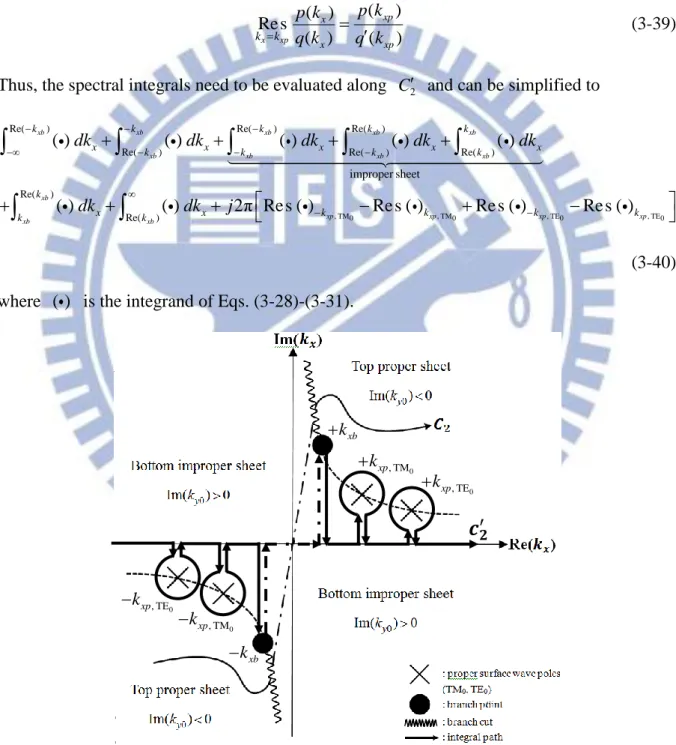
3.2.4 Discussion of Integration Contours
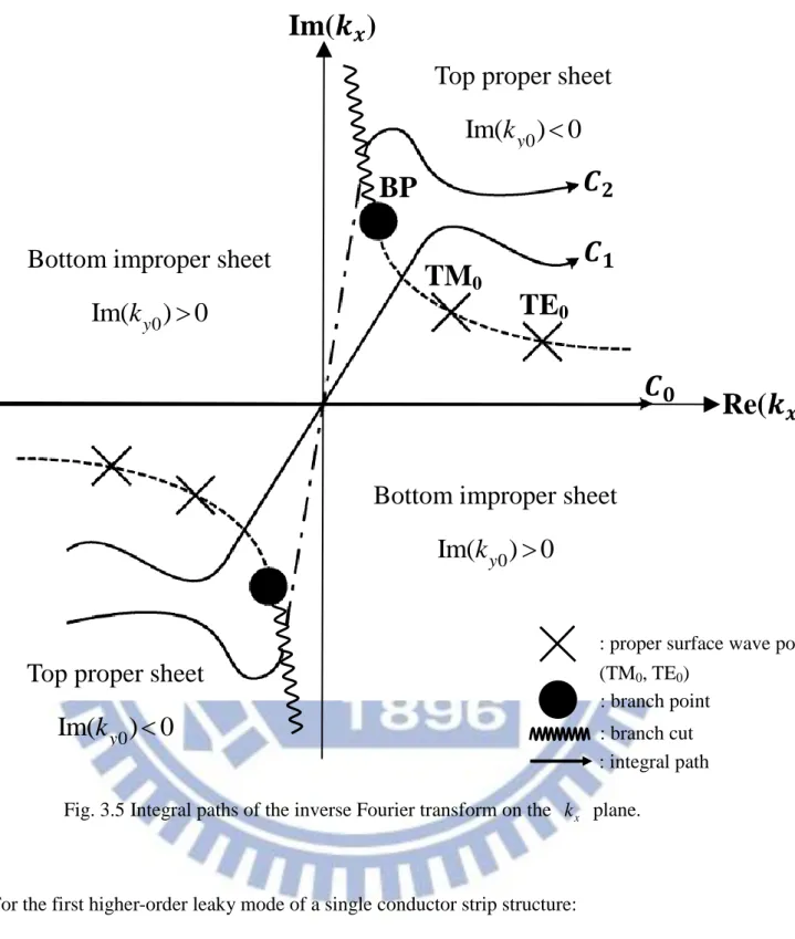
The main feature of interest in the spectral-domain analysis is the appropriate path of integration used to compute the matrix elements listed in (3-28)-(3-31) from which the propagation constant kz of a specific wave mode is to be found. Since the path is an open contour in the kx plane, from to , different solutions for kz are possible depending upon the choice of the integration contour. The conventional path, which lies along the real axis in the complex kx-plane (contour C0 of Fig. 3.5), yields the solution for the proper (bound) mode. The other two paths C1 and C2 in Fig. 3.5 are used to obtain leaky-mode solutions [15]. The absence of a ground plane allows the TM0 and the TE0
surface-wave modes to exist in the single-conductor strip structure [6]. Because both of the TM0 and the TE0 surface-wave modes exist for a dielectric slab structure (see Appendix D), so
two proper surface-wave poles of
0 , TM xp k and 0 , TE xp
k are present in the kx plane. As seen in Fig. 3.5, the path C1 detours around the poles of the integrand in the kx plane that correspond to the TM0 and the TE0 surface-wave modes of the dielectric slab structure, and
lies entirely on the top Riemann sheet of the kx plane, which is the proper sheet for the vertical wavenumber k y [16]. This path is used to obtain the solution for a leaky mode that has leakage into only the TM0 and the TE0 surface waves [8]. In order to yield the solution for
a leaky mode that energy leaks into both the space wave and the surface wave, the path C2 is utilized. This path lies partly on the improper sheet of the kx plane in the region between the branch cuts and includes both proper surface-wave poles for the TM0 and the TE0 modes [6].
22
For the first higher-order leaky mode of a single conductor strip structure:
1) propagation constant kz j (3-33) 2) ky0 k02 kx2kz2 , (proper sheet "", improper sheet "+") (3-34) 3) branch points (ky0 0): kxb k02 kz2 (3-35) These branch points define a two-sheeted Riemann surface in the kx plane. Using the
Sommerfeld choice for defining the corresponding branch cuts,
: integral path
BP
TM
0TE
0Im(
)
Re(
)
Bottom improper sheet
0
Im(
k
y) 0
Bottom improper sheet
0
Im(
k
y) 0
Top proper sheet
0
Im(
k
y) 0
Top proper sheet
0
Im(
k
y) 0
Fig. 3.5 Integral paths of the inverse Fourier transform on the kx plane. : branch cut : branch point
: proper surface wave poles (TM0, TE0)
23
2 2 2
0 0
Im(ky )Im k kx kz 0, the two sheets correspond to the vertical wavenumver 0
y
k being proper (imaginary part negative) and improper (imaginary part positive). The derivation is detailed in Appendix E.
4) TM0 poles: kxp, TM0 ks2, TM0 kz2 (3-36)
where
0
, TM
s
k is the wavenumber associated with the TM0 surface wave mode of the
dielectric slab structure.
5) TE0 poles: kxp, TE0 ks2, TE0 kz2 (3-37)
where
0
, TE
s
k is the wavenumber associated with the TE0 surface wave mode of the
dielectric slab structure.
For the integration of the products in Eqs. (3-28)-(3-31), the Green’s functions meet poles along the kx integral path. These poles are encountered when the denominator of Ze
or Zh is equal to zero. The zeros of the denominators of Ze and Zh correspond to the odd TM and odd TE surface wave modes in the dielectric slab waveguide, respectively. That is, the zeros of the denominators of Ze and Zh give the phase constant of the surface waves ( 0 , TM s k and 0 , TE s
k ) existing in the dielectric slab waveguide. Substituting
0 , TM s k into Eq. (3-36) and 0 , TE s
k into Eq. (3-37), we obtain the locations of the TM0 and TE0 surface wave
poles ( 0 , TM xp k and 0 , TE xp
k ) in the complex kx plane. By further deforming the path C2 in Fig. 3.6, we obtain a simple contour C2 that encloses
0 , TM xp k and 0 , TE xp k in the residue
sense. This means that the integrands of Eqs. (3-28)-(3-31) involve four residual contributions which correspond physically to excitation of the TM0 and TE0 surface waves; therefore we
24
can rearrange each of them as the quotient form as follows:
( ) ( ) ( ) ( ) ( ) x x x x x p k J k Z k J k q k (3-38) where p and q are both analytic at surface wave poles kxp, and p k( xp)0, q k( xp)0,
( xp) 0
q k . It can be shown that the residue is
Re s ( ) ( ) ( ) ( ) x xp xp x x xp k k p k p k q k q k (3-39)
Thus, the spectral integrals need to be evaluated along C2 and can be simplified to
, TM0 , TM0
Re( ) Re( ) Re( )
Re( ) Re( ) Re( )
Re( ) Re( ) improper sheet ( ) ( ) ( ) ( ) ( ) ( ) ( ) 2π Re s ( ) Re s ( ) Re s xb xb xb xb xb xb xb xb xb xb xp xp xb xb k k k k k x k x k x k x k x k x x k k k k dk dk dk dk dk dk dk j
, TE0 , TE0 ( ) Re s ( ) xp xp k k (3-40) where ( ) is the integrand of Eqs. (3-28)-(3-31).0 , TM xp k 0 , TE xp k xb k xb k 0 , TM xp k 0 , TE xp k
25
3.2.5 Numerical Results
Fig. 3.7 plots the normalized phase constant k0 and the normalized attention constant k0 against the frequency of the first higher order mode of the single conductor strip structure with and for different strip widths. Because of the resonance of the transverse currents, the leaky region obviously shifts to a higher frequency for a narrow strip. Also, a narrow strip increases the attention constant.
Fig. 3.7 Behavior of the normalized phase constants and the normalized attenuation constants as a function of frequencies for the first higher order mode of the single conductor strip structure with and for different strip widths.
26
Fig. 3.8 plots the normalized phase constant k0 and the normalized attention constant k0 against the frequency of the first higher order mode of the single conductor strip structure with and for different dielectric constants. A substrate with a high dielectric constant will rapidly increase the normalized phase constant. Increasing the dielectric constant of the substrate also increase the attenuation constant.
Fig. 3.8 Behavior of the normalized phase constants and the normalized attenuation constants as a function of frequencies for the first higher order mode of the single conductor strip structure with and for different dielectric constants.
27
Fig. 3.9 plots the normalized phase constant k0 and the normalized attention constant k0 against the frequency of the first higher order mode of the single conductor strip structure with and for different substrate thicknesses. When the thickness of the substrate increases, the normalized phase constant increases, since the effective strip width is reduced by the fringing effect. The attenuation constant of a thin substrate is less than that of a thick substrate. Most of the energy is focused under the strip when the dielectric constant is high or the substrate is thick. The energy leaks out to the air more easily if the thickness or the dielectric constant of the substrate is lower or smaller.
Fig. 3.9 Behavior of the normalized phase constants and the normalized attenuation constants as a function of frequencies for the first higher order mode of the single conductor strip structure with and for different substrate thicknesses.
28
Chapter 4
Antenna Design, Simulation and Measurement
Broadband, high gain, and frequency-scanning are the main features of leaky wave antennas [9]. In some applications, such as point-to-point communication, the frequency-scanning characteristic is undesired. In this chapter, we use a single-conductor strip leaky wave antenna, which is proposed in [6]. Unlike other leaky-wave antennas, whose main beam changes according to frequency, the single-conductor strip leaky-wave antenna has a fixed main beam in the end-fire direction over a broadband region. Compared to the resonant antennas such as microstrip patch antenna and dipole antenna, whose radiation patterns are in the broadside direction, the pattern feature of single-conductor strip leaky-wave antenna is useful in some applications that require a main beam in the end-fire direction. Finally, to alleviate the problem of a large back lobe [17], the feeding structure of the single-conductor strip leaky-wave antenna is modified with two broadband planar baluns [18]. The simulated and measured results are also presented in this chapter.
4.1 DESIGN OF SINGLE-CONDUCTOR STRIP LEAKY-WAVE
ANTENNA
4.1.1 Broadband Planar Feeding Structure
As described above, the single-conductor strip structure has only a single-conductor strip on a substrate without a practical ground plane. For the first higher-order leaky mode in this structure, an infinite virtual PEC boundary is assumed at the center of the strip, in which the longitudinal currents are odd-symmetric and the transverse currents are even-symmetric with respect to the center [6]. As shown in Fig. 4.1, these current distributions help us design an appropriate feeding structure which generates two out-of-phase currents to feed this
29
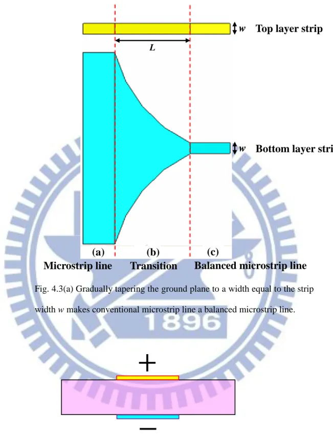
single-conductor strip structure and thus excites the first higher order leaky mode. As shown in Fig. 4.2, a broadband planar feeding structure which consists of a conventional microstrip line、a microstrip-to-balanced-microstrip-line transition、a balanced-microstrip-line T-junction power divider and one set of the balanced microstrip lines is changed to form the inverted balanced microstrip lines is developed for the first higher-order leaky mode of the single-conductor strip line [6]. As shown in Fig. 4.3, gradually tapering the ground plane to a width equal to the strip width w makes conventional microstrip line a balanced microstrip line, with a strip of positive voltage on the upper side of the substrate and a strip of negative voltage on the lower side of the substrate.
y
z
x
PEC symmetry plane
To excite the first higher-order leaky mode
w
h
No ground
Fig. 4.1 An appropriate feeding structure which generates two out-of-phase currents is used to feed the single-conductor strip structure and thus excites the first higher order leaky mode.