Fabrication and Electrical Characteristics of the
Nanocrystal Nonvolatile Memory Devices
:
:
Fabrication and Electrical Mechanism of the Nanocrystal
Nonvolatile Memory Devices
Student
Chih-Wei Hu
Advisor Dr. Tseung-Yuen Tseng
Dr. Ting-Chang Chang
A Dissertation
Submitted to Department of Electronics Engineering and
Institute of Electronics
College of Electrical and Computer Engineering
National Chiao Tung University
in partial Fulfillment of the Requirements
for the Degree of
Doctor of Philosophy
in
Electronics Engineering
July 2010
I
:
:
floating-gate
II
9 10
2.4 104
4.5×1012cm-2)
III
5-6 奈米 and 3.2×1012cm-2。 7
800
IV
Fabrication and Electrical Characteristics of the
Nanocrystal Nonvolatile Memory Devices
Student
Chih-Wei Hu Advisor
Dr. Tseung-Yuen Tseng
Dr. Ting-Chang Chang
Department of Electronics Engineering and Institute of Electronics,
National Chiao Tung University, Hsinchu, Taiwan
Abstract
In conventional memory devices, poly-silicon is used as the ―floating-gate‖ to
store charge. However, the conventional floating-gate non-volatile memory device
has faced the challenge of reliability due to the requirement of down-scaling device.
The scaled tunneling oxide is difficult to prevent the stored charge in the floating-gate
from tunneling back into the Si-substrate. To improve the retention time of
conventional floating-gate memories, nanocrystal memory devices have been
proposed. In the nanocrystal structure, the device can store charge in distributed
charge trapping centers. Even if the leakage path is formed in the tunneling oxide, the
device still can keep enough charge for the correct data of logic circuit.
In the thesis, the nanocrystal memory devices using Co and Ni as charge trapping
center have been fabricated and studied due to the higher work-function, better gate
V
methods to form nanocrystal structures are by the self-assembled characteristic of thin
film, aggregation by the over-saturation, and different oxidized tendency between
elements. Many improvements of the aforementioned methods have been discussed
and proposed.
In the self-assembled system, a novel nanocrystal structure has been fabricated
by annealing the Ge-incorporate NiSi (NiSiGe) film. After a RTA process, it is found
that the annealed NiSiGe film shows a larger nanocrystal size (~8-9nm) and lower
density distribution (3.02×1011cm-2) than the conventional NiSi nanocrystal. The large size and lower density of nanocrystal are due to the internal Ge elements that provide
an easier crystallization and enhance the nanocrystal formation. Furthermore, the
NiSiGe nanocrystal memory device shows a 9V of memory window under ± 10V
operation in capacitance-voltage measurement due to the improved nanocrystal
formation process. In the retention test, the NiSiGe nanocrystal memory device also
has a 2.4V of memory window after 104 sec measurement.
Ion implantation can control the nanocrystal aggregation sites and density by
adjusting the energy and dosage of the implantation. However, the implantation
method also brings a drawback of oxide damage. Therefore, a co-evaporation has
been proposed to fabricate nickel nanocrystal structure. The co-evaporation to form
VI
annealing process, respectively. The distributed nucleation sites provided by the
co-evaporation bring a double layer distribution. The double layer nanocrystal device
shows an 8V memory window due to a higher nanocrystal density. However, the 800 ℃-annealed device has an extra high density distribution (~4.5×10¹²
cm-2) even if the device only has single layer structure. In the retention test, the 800 ℃-annealed
sample also can keep a 2.3V memory window due to a improvement of dielectric
layer surrounded the nanocrystal.
Several literatures have studied the segregation of the nanocrystal by the
difference of the oxidation free energy between the elements. A reactive sputtering
has been used to fabricate the Co nanocrystal structure to avoid the over-oxidation of
the charge-trapping layer. In the reactive sputtering process, the deposited CoSi2 thin
film is oxygen-doped or partially oxidized. After a 700℃ RTA process, it can be
found that Co nanocrystal were aggregated on the tunneling oxide obviously. The size
and density of the nanocrystal are about 5-6nm and 3.2×1012cm-2, respectively. The nanocrystal memory device shows a 7V memory window under ± 15V operation. In
the retention characteristic, the memory device also can keep a 3.1V memory after 104 sec measurement.
Low-temperature oxide deposited technology is critical for the next generation
VII
oxidation has been studied. The decomposition of HNO3 as powerful oxidizing agent
can provide a high concentration of atomic oxygen to oxidize the immersed metal or
semiconductor layer. It can be found that the CoSi2 nanocrystal memory device with
nitric acid oxidized ZrO2 film as tunneling oxide shows a 10V memory window and
2.1V of memory window in the retention measurement. The nitric acid oxidation is
advantageous to improve the thermal budget issue of the thermal oxide demand of the
conventional nanocrystal memory devices because the higher fabrication temperature
of the NVM devices is determined by the nanocrystal.
Keywords: Nanocrystal; Nonvolatile memory; Nickel silicide; Cobalt silicide; Nitric
X
Contents
Chinese Abstract
---IEnglish Abstract
---IVAcknowledgement---VIII
Contents
---XFigure Captions
---XIIIChapter 1 Introduction
1.1 Overview of floating-gate memory device ---1
1.1.1 Operation of the floating-gate memory device ---2
1.1.2 Challenge of the conventional floating-gate structure ---2
1.2 The solutions for the down-scaling memory device---3
1.2.1 SONOS structure memory device ---3
1.2.2 Nanocrystal structure memory device ---6
1.3 The further Study of the nanocrystal memory device ---7
1.3.1 Formation of the nanocrystal structure---7
1.3.2 The material of the nanocrystal ---9
1.4 Motivation ---10
Chapter 2 Basic Principles of Nonvolatile Memory
2.1 Introduction---152.2 Basic write and erase mechanisms ---16
2.2.1 Energy band diagram during write and erase operation---16
2.2.2 Carrier transport mechanisms ---17
2.3 Basic reliability of nonvolatile memory ---23
2.3.1 Retention ---23
2.3.2 Endurance ---24
2.3.3 Self-converging---25
2.4 Basic physical characteristic of nanocrystal nonvolatile memory ---25
2.4.1 Quantum confinement effect ---26
2.4.2 Coulomb blockade effect ---26
Chapter 3 Fabrication and Memory Effect of Ni Nanocrystal by
Co-evaporating with Dielectric Layer
XI
dielectric layer for the memory application ---34
3.1.1 Introduction---34
3.1.2 Experiment---35
3.1.3 Results and discussion---36
3.1.4 Conclusion---39
3.2 High density Ni nanocrystal formed by co-evaporating Ni and SiO2 pellets for the nonvolatile memory device application ---40
3.2.1 Introduction---40
3.2.2 Experiment---40
3.2.3 Results and discussion---41
3.2.4 Conclusion---44
3.3 Formation of double- and single- layer Nickel nanocrystal embedded in Si3N4 dielectric layer by co-evaporating Ni and Si3N4 pellets ---44
3.3.1 Introduction---44
3.3.2 Experiment---45
3.3.3 Results and discussion---45
3.3.4 Conclusion---47
Chapter 4 Fabrication and Memory Effect of Co Nanocrystal by
Sputtering in the O
2/N
2Ambiance
4.1. Cobalt nanocrystal embedded in silicon oxide fabricated by incorporating oxygen elements during sputtering process ---614.1.1 Introduction---61
4.1.2 Experiment---62
4.1.3 Results and discussion---63
4.1.4 Conclusion---67
4.2. Co nanocrystal embedded in Si3N4 dielectrics by sputtering in the N2 ambiance---67
4.2.1 Introduction---67
4.2.2 Experiment---68
4.2.3 Results and discussion---68
4.2.4 Conclusion---69
Chapter 5 Fabrication and Investigation on the Application of
Ni-Si-Ge Nanocrystal for Nonvolatile Memory
5.1. Enhancement of NiSi-based nanocrystal formation by incorporating Ge elements for nonvolatile memory devices ---79XII
5.1.2 Experiment---80
5.1.3 Results and discussion---81
5.1.4 Conclusion---85
5.2. Formation of the distributed NiSiGe nanocrystal nonvolatile memory formed by rapidly annealing in N2 and O2 ambient ---86
5.2.1 Introduction---86
5.2.2 Experiment---86
5.2.3 Results and discussion---87
5.2.4 Conclusion---90
5.3. Improved aggregation of the NiSiGe nanocrystal by pre-capping oxide method for nonvolatile memory device application ---91
5.3.1 Introduction---91
5.3.2 Experiment---92
5.3.3 Results and discussion---92
5.3.4 Conclusion---95
Chapter 6 Nitric Acid Oxidation for the Tunneling Oxide Application
on CoSi
2Nanocrystal Nonvolatile Memory
6.1. Nitric acid oxidation of Si for the tunneling oxide application on CoSi2 nanocrystal nonvolatile memory ---1086.1.1 Introduction---108
6.1.2 Experiment---109
6.1.3 Results and discussion---110
6.1.4 Conclusion---115
6.2. ZrO2 formed by nitric acid oxidation as the tunneling oxide of cobalt-silicide nanocrystal nonvolatile memory device ---116
6.2.1 Introduction---116
6.2.2 Experiment---117
6.2.3 Results and discussion---118
6.2.4 Conclusion---122
Chapter 7 Conclusion Remarks
---134Chapter 8 Future work
---137References
---138Vita
---155XIII
Figure Captions
Chapter 1
Fig. 1-1 The floating-gate memory device. ---11
Fig. 1-2 The 2009 ITRS roadmap.---11
Fig. 1-3 The SONOS and nanocrystal memory devices.---12
Fig. 1-4 The BE SONOS memory devices.---12
Fig. 1-5 2-bit per cell for SONOS memory device.---13
Fig. 1-6 Double layer NC memory device. ---13
Fig. 1-7 Schematic illustration of the driving forces in the self-assembly process [1.17].---14
Chapter 2
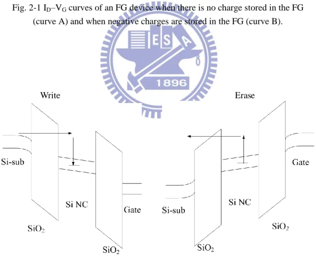
Fig. 2-1 ID–VG curves of an FG device when there is no charge stored in the FG (curve A) and when negative charges are stored in the FG (curve B).---28Fig. 2-2 The write and erase mode of the FG memory device.---28
Fig. 2-3 The diagram of tunneling effect.---29
Fig. 2-4 The band-diagram of FN tunneling.---29
Fig. 2-5 Band gap of the High-K dielectrics.---30
Fig. 2-6 Source-side hot-electron writing. ---30
Fig. 2-7 Channel hot electron injection. ---31
Fig. 2-7 Band to band hot electron injection in p-channel MOSFET.---31
Fig. 2-8 Band to band hot hole injection in n-channel MOSFET.---32
Fig. 2-9 The operation of negative gate erase.---32
Fig. 2-10 Typical endurance characteristic of memory devices.---33
Fig. 2-11 The diagram of the erased-threshold voltage distribution.---33
Chapter 3
Fig. 3-1 The process of the co-evaporating process.---49Fig. 3-2 (a) cross-section TEM micrographs and (b) C-V result of the NC memory devices formed by annealing at 700 ℃ for 1 min.---49
Fig. 3-3 (a) The Ni 2p and (b) O 1s XPS spectra of the charge trapping layer after 700℃ thermal annealing. (c) The forming process of the Ni NC structure during thermal annealing.---50
Fig. 3-4 (a) Charge retention and (b) endurance characteristics of the Ni NC formed by annealing at 700℃ for 1 min.---51
Fig. 3-5 (a) The cross-section TEM micrographs and (b) forming process of the Ni NC at 800℃ annealing for 1 min.---52
XIV
Fig. 3-6 The C-V result of the Ni NC memory device formed by the 800℃ annealing for 1 min.---53 Fig. 3-7 (a) Charge retention and (b) endurance characteristics of the Ni NC formed
by annealing at 800℃for 1 min.---53 Fig. 3-8 The comparison of gate current density (J-V) and leakage mechanism between the memory devices.---54 Fig. 3-9 (a) The cross-section and (b-d) plane-view TEM images of the Ni and SiO2
mixed film after 800℃ rapidly thermal annealing. The size distribution can be seen in the dispersion of NC size.---55 Fig. 3-10 (a&b) The Ni 2p XPS spectra and O 1s XPS spectra of the charge trapping layer after thermal annealing.---56 Fig. 3-11 (a) High-frequency C–V characteristic and (b) J-V characteristic of the Ni
NC memory device.---56 Fig. 3-12 (a) Charge retention characteristic and (b) endurance characteristic of the
formed Ni NC memory device.---57 Fig. 3-13 (a&b) The cross-section TEM micrographs of the Ni and Si3N4 mixed film
after 700 and 800℃ rapidly thermal annealing, respectively. ---57 Fig. 3-14 (a) The Ni 2p and (b) N 1s XPS spectra of the charge trapping layer after
700℃ thermal annealing. ---58 Fig. 3-15 (a&b) High-frequency C-V characteristics of the Ni NC formed by
annealing at 700 and 800℃, respectively.---59 Fig. 3-16 (a&b) High-frequency C-V characteristics of the Ni NC formed by
annealing at 700 and 800℃, respectively.---59 Fig. 3-17 (a&b) The retention of the Ni NC formed by annealing at 700 and 800℃,
respectively. ---60
Chapter 4
Fig. 4-1 (a) The cross-section TEM image and (b) the Co 2p XPS spectra of the Co
NC formed by the sputtering in Ar/O2 (24 sccm/5 sccm) ambient. The NC
forming process is 700 ℃ RTA in N2 for 1min.---70
Fig. 4-2 (a) The C-V characteristic and (b) retention characteristics of the Co NC formed by the sputtering in Ar/O2 (24 sccm/5 sccm) ambient.---71
Fig. 4-3 (a) The C-V characteristic and (b) retention characteristics of the Co NC formed by annealing by 800℃ annealing temperature for 1 min.--- --72 Fig. 4-4 The plane-view TEM image of the NC formed by (a) 700 and (b) 800℃ RTA process, respectively.---73 Fig. 4-5 The comparison of the current density-voltage (J-V) characteristic between
XV
the samples.---74 Fig. 4-6 The comparison of memory window about the Co NC devices with 2, 5, 7
and 10 sccm of O2 flow rate during the sputtering process. ---74
Fig. 4-7 (a)-(d) The cross-section TEM images of the Co NC memory devices formed with 2, 5, 7 and 10 sccm of O2 flow rate during the sputtering
process, respectively. ---75 Fig. 4-8 The comparison of the Co 2p XPS spectra about the Co NC devices with 2,
5, and 7 of O2 flow rate during the sputtering process.---76
Fig. 4-9 The C-V hysteresis of the CoSi2 thin film deposited at (a) 5sccm (b)
10sccm (c) 20sccm of the nitrogen flow rate.---77 Fig. 4-10 The cross-sectional TEM images of the CoSi2 thin film deposited at (a)
5sccm (b) 10sccm (c) 20sccm of the nitrogen flow rate.---78
Chapter 5
Fig. 5-1 Process flow and device structure of this study.---96 Fig. 5-2 The plane-view and cross-section TEM micrographs of the annealed (a)
NiSi and (b) NiSiGe film.---96 Fig. 5-3 5-3 (a) The Ni 2p3/2 XPS spectra of the annealed NiSi and NiSiGe mixed film. (b) The Ge 3d XPS spectra raw data and the fitting data of NiSiGe film after thermal annealing.---97 Fig. 5-4 (a) Raman spectroscopy and (b) EDS of the NiSiGe film after thermal annealing.---98 Fig. 5-5 The speculated picture for the formation process of the NiSiGe NC during
rapidly thermal annealing (RTA) process.---99 Fig. 5-6 C–V characteristics (1 MHz) of the MOIOS structures: (a) with NiSi and (b)
NiSiGe NC as the trapping layer of the memory device. ---99 Fig. 5-7 Retention characteristics of the (a) NiSi and (a) NiSiGe NC memory
devices ---100 Fig. 5-8 Endurance characteristics of the (a) NiSi and (b) NiSiGe NC memory devices.---100 Fig. 5-9 The cross-section TEM micrographs of the NiSiGe film after the (a) RTA and (b) RTO process for 60 sec.---101 Fig. 5-10 The C–V characteristics of the MOIOS structures: NiSiGe NC formed by (a)
RTA and (b) RTO process.---101 Fig. 5-11 The endurance characteristic of the NiSiGe film after (a) RTA and (b) RTO process.---102 Fig. 5-12 The retention characteristic of the NiSiGe film after (a) RTA and (b) RTO
XVI
Fig. 5-13 The Ge 3d XPS spectra of the NiSiGe film after (a) RTA and (b) RTO process.---103 Fig. 5-14 The J-V characteristics of the NiSiGe film after (a) RTA and (b) RTO process. ---104 Fig. 5-15 The SIMS analysis of the NiSiGe NC formed by RTO process.---104 Fig. 5-16 The cross-section TEM micrographs of the NiSiGe thin film.---105 Fig. 5-17 The EDS analyses of the formed NC structure. Region a and b is the space and NC region, respectively.---106 Fig. 5-18 The C-V results of the NiSiGe thin film (a) without, (b) with 10nm and (c) with 20 nm pre-capped oxide before the thermal annealing process, respectively. ---107 Fig. 5-19 Retention and endurance of the NiSiGe thin film (a&c) with 10nm and
(b&d) with 20nm pre-capped oxide before the thermal annealing process. ---107
Chapter 6
Fig. 6-1 The process flow proposed in this work.---124 Fig. 6-2 (a) C-V and (b) J-V characteristics of MIS structure using the NAO-SiO2
layer as the gate oxide. The inset-of 2(a) is the cross-section TEM image of the MIS structure.---124 Fig. 6-3 The Si 2p XPS spectra of (a) the as-deposited Si film, the NAO-SiO2 (b)
before and (c) after the RTA set at 700 for 30 sec, respectively. ---125 Fig. 6-4 The cross-section TEM image of the formed memory structure using the
NAO-SiO2 as device tunneling oxide.---125
Fig. 6-5 (a&b) The Co 2p3/2 and Si 2p XPS spectrum of the charge-trapping layer after the RTA at 700 for 30sec. (c&d) The EDS analyses of the compositions of the NAO-SiO2 and NC.---126
Fig. 6-6 The SIMS analysis of the CoSi2 NC memory device.---127
Fig. 6-7 The (a) C-V and (b) J-V curve of the MOIOS structure using the NAO-SiO2
as device tunneling oxide.---127 Fig. 6-8 The (a) retention and (b) endurance characteristics of the MOIOS structure
using the NAO-SiO2 as tunneling oxide.---128
Fig. 6-9 The (a) XPS and (b) oxidation process of the ZrO2 film.---128
Fig. 6-10 The (a) C-V and (b) J-V results of the MIS structure.---129 Fig. 6-11 Memory effect obtained from C-V characterization and (b) current density measurement of the formed CoSi2 NC memory device.---130
Fig. 6-12 The (a) retention and (b) endurance characteristics of the formed CoSi2
XVII
Fig. 6-13 The (a) TEM and (b) AES analyses of the CoSi2 NC memory device using
the nitric acid oxidized ZrO2 as the tunneling oxide.--- 132
1
Chapter 1
Introduction
1.1 Overview of floating-gate memory device
Recently, floating-gate (FG) structure devices are the mainstream technology for
the nonvolatile memory. It was invented by Kahng and Sze at Bell Labs in 1967 [1.1].
The FG structure is shown in the Fig 1-1. A modified FG structure device called flash
memory was proposed by Fusio Masuoka et al in 1987, which is the most important
one member of the FG family [1.2]. The structure and operation of the flash are
similar as the original FG memory device. However, the flash memory device uses an
additional erase contact, which can reduce the erase time by a block erase mode. In
addition, the flash memory devices can be classified into two types, NOR and NAND
flash memories, according to their functions and advantages. The NOR Flash offers
faster read speed and random access capabilities, making it suitable for code storage
in devices. In contrast, the NAND memory, which offers faster write/erase capability
and higher density, is typically used for storing large quantities of data [1.3].
1.1.1 Operation of the floating-gate memory device
The basic operation of the memory device is by applying positive voltage on the
control gate to promote the electron in the channel to pass through the tunneling oxide
2
induce a positive threshold voltage shift (△ VT) as the ―1‖ state for the memory
device. In contrast, the stored electrons will tunnel back to the Si substrate when a
negative voltage is applied to the control gate electrode in the erase mode. Then, the △ VT is think as the ―0‖ state of the memory device. Based on the advantages of the
FG structure such as low-power, easy process and compatibility with the current
complementary-metal-oxide-semiconductor (CMOS) process, FG nonvolatile
memory structures have attracted much attention on the portable products especially
for the cell phone, mp3 player and digital camera.
1.1.2 Challenge of the conventional floating-gate structure
According to the 2009 International Technology Roadmap for Semiconductors
(ITRS) for flash memory as shown as the Fig. 1-2 [1.4], tunneling oxide thickness
must be thinner than 8-nm to assure enough gate control ability to reduce the
short-channel effect. In the vertical scaling, the thinner tunneling oxide leads to high
leakage current and poorer charge retention for the memory device. Furthermore, after
endurance test, traps can be generated in tunneling oxide, which may induce a leak
path in the tunneling oxide and results in a serious leakage current. In addition, in the
lateral scaling limit, the space between devices is reduced [1.5]. When one device is
written or erased, the nearby memory cell may also be written or erased. Therefore,
3
1.2 The solutions for the down-scaling memory device
To overcome the trade-off problems of the FG memory, discrete trapping center
instead of electrically continuous poly-silicon FG have been received much attention
in the recent years. Unlike to the poly-silicon gate, the charge-trapping layer memory
devices stored charges in the distributed centers. Therefore, even if an intrinsic defect
or extrinsic defect chain exists in the tunneling oxide, the memory device still can
provide correct information because only partial stored charge will be lose. The main
structures of discrete charge-trapping center are poly-silicon/oxide/nitride/oxide/Si
(SONOS) memory and nanocrystal (NC) memory. Fig. 1-3 illustrates the structure of
the SONOS and NC memory device. By using the charge-trapping layer structure, the
operational voltage of the device can be lower and the operational speed of the device
can be improved further.
1.2.1 SONOS structure memory device
An original idea for the SONOS device is proposed by Wegener et al in 1967
[1.6]. Wegener using an additional silicon nitride placed in between the control gate
and tunneling oxide to be charge-trapping layer. The silicon nitride can provided a
trap density of the order 1018-1019 cm-3 to cause a △ VT for the memory device. In
the early 1970s, the initial device structure was p-channel metal-nitride-oxide-silicon
4
(~45nm) silicon nitride as the charge storage layer. Due to a serious leakage current
of the device, a thicker tunneling oxide is essential, which also cause the write/erase
voltages of device operation need to be 25-30V. In the early 1990s, n- and p-channel
device can be operated by a write/erase voltage of 5-12V due to the improvement of
the fabrication. To improve the disadvantages of the original MNOS device, the
SONOS structure was proposed. The basic operation and charge storage mechanism
are similar as the MNOS device. The SONOS have attracted a lot of attention due to
its advantages of include a reduced cell-to cell interference, a high speed operation, a
lower voltage operation, improved cycling endurance, and elimination of
drain-induced turn-on [1.7]. The SONOS structure uses a poly-silicon gate to replace
the Al gate due to the self-aligned process. An additional blocking oxide between the
control gate and nitride also can restrain the programmed charge to lose into the gate
electrode. In the recent year, High-K material such as Al2O3, HfO2 and ZrO2 has also
been applied into the SONOS memory device [1.8]. By using a High-K material as
the device blocking oxide, the applied gate voltage during write/erase operation will
mostly drop in the tunneling oxide. A higher tunnel current can improve the
write/erase speed of the device. Also, the use of High-K material can improve the
gate coupling conditions because silicon nitride will share the higher applied gate
5
charge-trapping layer, a band-gap engineering (BE) has been proposed as shown as
the Fig. 1-4. By controlling Si/N ratio of the nitride layer, the trap density and band
gap of the charge trapping layer can be adjusted [1.9]. The BE SONOS device shows
an excellent endurance and retention characteristics. In addition, in the replacement
of charge storage layer, a High-K material also is a choice by adjusting the band-gap
of the charge trapping layer or the band offset between the tunneling
oxide/charge-trapping layer and blocking oxide/charge-trapping layer [1.10-1.11]. In
the gate electrode, a metal gate will be next leading role due to the High-K material
needs a metal gate to reduce the mobility lowing effect of device. The use of metal
gate also can provide energy-band engineering for the SONOS. For example, using a
higher work-function material such as TaN, NiSi2 or Mo, the tunnel current from the
control gate can be reduced during the erase operation. Therefore, an erase saturation
of the device will be avoided. In the device structure, 3-D SONOS such as
double-gate, tri-gate and gate-all-around is critical for the next generation memory
device [1.12-1.15]. However, the theoretical modeling for the devices is difficult due
to the non-uniform electric field distribution and non-uniform charge storage. The
SONOS device also can store 2-bit by a cell due to the localization of trapped charge.
By channel hot electron injection (CHI) to program device, charge can be controlled
6
devices will have four kind of VT to be four stored states.
1.1.2 Nanocrystal structure memory device
The idea of NC structure using discrete nanodots as the charge-trapping centers
is similar as SONOS memory device. When a thin film (~6-8nm) was deposited, a
followed annealing process may induce the thin film to aggregate and form NC to
reduce the system energy. The NC also can provide trapping sites by itself or the traps
created by NC and its surrounded oxide. The advantages of the NC include immunity
to stress induce leakage current (SILC), lower power consumption, higher write/erase
speed and lower process cost. The NC nonvolatile memory device also can be 2-bits
storage because the device operated by charge trapping mode, which is similar as
SONOS device. In the research of NC, to control the size and density of NC is
important because the uniformity of NC becomes critical when the device is
down-scaling. Therefore, several high-density NC technologies have been proposed to
improve the NC characteristic [1.16-1.17]. A double NC layer structure also attracts
much attention due to the higher NC density [1.19-1.20]. By choosing a different NC
material, a band-gap engineering of double NC as shown as Fig. 1-6 can improve the
performance of the memory device because the bottom layer NC with a lower
work-function can restrain the stored charge to loss [1.21]. Also, High-K material is
7
also combine with the SONOS structure to create more charge-trapping sites for the
memory application.
1.3 The further study of the nanocrystal memory device
To apply NC structure into the memory device, more detailed studies are very
critical. A suitable can reduce the NC fabricating cost and obtain excellent NC
uniformity, which bring a better electrical performance of the memory devices.
1.3.1 Formation of the nanocrystal structure
Generally, the most common NC fabricating methods are by self-assembled
characteristic of thin film, selective oxidation, and over-saturation of the doped
elements.
(a) Self-assembled system:
Self-assembled system has been studied for the nanodot or nanowire structure
extensively. Fig. 1-7 is the schematic illustration of the driving forces in the
self-assemble system [1.23]. The most importation driving force for the
aggregation of NC is the relaxation of film stress. To reduce the intrinsic energy of
the system, the atom will bond and form a sphere. However, the aggregation of the
atoms is limited by the surface mobility. The surface mobility is depended on the
diffused ability of elements. A rapidly thermal annealing (RTA) process after the
8
bond. The density and size of the NC is also depended on the annealing process.
The first step of the aggregation is the diffusion of initial elements during the
thermal annealing. Then, nuclei are nucleated due to the collisions. The NC grows,
where by diffusing atoms bond to existing nuclei. As the NC grows to touch the
nearby NC, the smaller NC will merge with larger NC. The density of NC will
decay and size of NC will be larger.
(b) Selective oxidation system:
In the case of SiGe system, during the oxidation process, the difference of
oxidized ability between Si and Ge cause the external oxygen elements tend to
react with the Si elements during the thermal oxidation process. It brings that a
selective oxidation process to enhance the Ge aggregation as the NC embedded in
SiO2 dielectrics layer. The chemical reaction process can also be used in the
silicide system as NiSi, CoSi and PtSi [1.24-1.25]. The advantage of the oxidation
process is the oxidation always brings a lower thermal-budget than the
self-assembled system due to the oxidation process can enhance the aggregation.
In addition, the formed NC have better size and density distribution. However, the
time or temperature during the oxidation process must be controlled carefully to
avoid over-oxidation.
9
The segregation of NC also can be procured by over-saturation mechanism. The
method is common in fabrication of optical devices. The process is to dope metal
or semiconductor ions into dielectric layer by an ions implantation. Based on each
dielectric material has its specific solid solubility, a followed annealing process
will cause the excess of dose will be segregated. The segregated dose will diffuse
in the dielectrics layer and form NC.
1.2.2 The material of the nanocrystal
With different applications, to find an adaptable material to satisfy the
requirements is a major subject. In addition, the uniformity and density of NC
distribution are the essential issue for the NC formation engineering. Generally, the
common material of the NC can be divided into (a) semiconductor (Si, Ge and GaAs)
(b) dielectric (GeO2, CoO and HfO2) and (c) metallic (Ni, Co, NiSi2 and Pt).
Semiconductor-based NC is first NC, which can avoid the issue of the metal
contamination but have a higher formation temperature. In addition,
semiconductor-based NC is potential to fabricate the optical devices such as laser or
solar cell due to that the band-gap of the NC can be controlled by quantum
confinement effect. In the dielectric NC, more charge storage sites such as the concept
of SONOS device will be created by distributed charge storage sites between the NC
10
disadvantages of the dielectric NC is its gate voltage coupling efficiency. The High-K
trapping layer may be the solution for the issue. The metallic NC has attracted much
retention because more charge storage sites can be provided due to the metal has more
density of states. The metallic NC also has a lower quantum confinement effect
compared with semiconductor-based NC. It is also believed that a high work-function
NC provided by the band engineering can restrain the stored charge to tunnel back to
channel and improve the device reliability characteristics.
1.2.3 Motivation
The FG memory faces a challenge in down-scaling device. Among the reported
literature, a structure with distributed NC as charge storage sites is considered a
potential solution to replace the conventional memory structure. Many different
researches of the NC such as the development of material, the improvement of
performance and the electrical operation of NC device have been reported in recent
years. The most important topic for the NC formation included easy process, lower
formation temperature and better NC distribution. In the thesis, several improved
11
Fig. 1-1 The floating-gate memory device.
12
Fig. 1-3 The SONOS and NC memory devices.
SiO
2SiO
2Si-sub
Gate
Si
3N
4N-rich
Si-rich
13
Fig. 1-5 2 bit per cell for SONOS memory device.
14
Fig. 1-6 Schematic illustration of the driving forces in the self-assembly process
15
Chapter 2
Basic Principle of Nonvolatile Memory
2.1 Introduction
The states of NVM memory can be defined by threshold voltage VT of the
transistor, charge displacements, or resistance change. If electrons have to be stored in
a cell of the memory, the △VT of a Flash transistor can be written as [2.1]:
FC T
C
Q
V
where Q is the charge weighted with respect to its position in the gate oxide, and the capacitances between the FG and control gate. Fig. 2-1 shows the △VT
between two states in a Flash memory. It can be found that the threshold voltage of
the memory cell is changed by charging the amount of electron or hole between the
gate and the channel, corresponding to the two states of the memory cell, i.e., the binary values (―1‖ and ―0‖) of the stored bit.
In this chapter, the write/erase mechanisms of the memory device will be
discussed by the relation between gate bias and energy band diagram of the transistors.
We also demonstrated the detailed operation of the device such as the tunneling
injection, channel hot electron injection, and band to band assisted electron/hole
16
retention and endurance tests have also been discussed.
2.2 Basic write and erase mechanisms
The nonvolatile memory device included NC and SONOS memories is changed
its state by writing or erasing the stored electrons. In exact definition for the memory
cells, ―erase‖ is to change the state of a group of memory cell and ―write‖ is to change
the state of one cell. However, the definition is too difficult to differentiate the
transmission of carrier. Therefore, we define when electrons are injected into
charge-trapping layer is called ―write‖ and when the stored charges are de-trapped to
silicon substrate is called ―erase‖.
2.2.1 Energy band diagram during write and erase operation
Fig. 2-2 illustrates the defined write/erase physical operation of a NC memory
device. In the write operation, a positive voltage is applied on gate electrode relative
to the p-type substrate, which forms an electron channel. Then the electrons tunnel
through the tunneling oxide into the charge-trapping layer and are stored in NC. Some
electrons not trapped in the NC are also possible to tunnel through a blocking oxide
into the gate electrode. The trapped electrons result in a △VT of the transistor. In the
erase operation, the gate electrode is on a negative voltage bias, the trapped electrons
can be de-trapped into the conduction band of the NC and then tunnel back to the
17
parameter to affect the erase speed of the device. To improve the erase speed of the
memory device, the holes tunnel becomes very important. In the erase operation, the
applied negative voltage bias also can enhance the holes tunnel from the substrate into
the NC and are partially trapped in the trapping layer. The △VT results from the
trapped electron and hole are neutralized.
2.2.2 Carrier injection mechanisms Tunneling Injection-
In 1924, De Broglie had proposed the matter wave or de Broglie wave theory.
The matter wave theory indicates that the motion of a particle can be thought as a
wave in the quantum size as shown as Fig. 2-3. Therefore, tunneling injection is
reasonable because a particle becomes possible to pass through wall or a barrier
motion of the wave. The Schrödinger equation provided by Erwin Schrödinger
accomplished the theoretical framework and calculates.
In the tunneling theory, tunneling probability is depended on electron barrier
height (φ(x)), tunnel dielectric thickness (d), and effective mass (me) inside the tunnel
dielectric [2-2].
18
possibility for the electrical devices especially when the device is down-scaled to
nanometer scale. For the memory device, several tunneling processes such as
Fowler-Nordheim tunneling (FN), Direct tunneling (DT), trap assistant tunneling
(TAT), modified Fowler-Nordheim tunneling (MFN) have also be studied successively.
Today, the tunneling processes also affected the operation and performance of the
memory device.
1. Fowler–Nordheim tunneling
The Fowler–Nordheim (FN) tunneling is the most important tunneling effect for
the memory device as shown as the Fig. 2-4. The FN tunneling always occurs in a
strong electric field (about 8–10MV/cm). In a strong electric field, the height and
thickness of the barrier is charged. Then, the electrons have more chance to pass
through the barrier wall from a metal or and semiconductor and arrive at the other
side of the barrier wall. By the Wentzel–Kramers–Brillouin (WKB) approximation
and free-electron gas model [2.3]. The equation of the FN tunneling can be obtained
as the followed as [2.4]:
qF
m
h
F
q
J
OX B B3
)
2
(
4
exp
16
2 3 2 1 2 2 2 3
In this equation, ФB is the barrier height,
OX
m
is the effective mass of the electron in the forbidden gap of the dielectric, h is the Planck’s constant, q is the electronic charge, and F is the electrical field through the oxide. The FN tunneling is
19
the original write and erase method for the FG memory device especially for a thicker
tunneling oxide. The write and erase by the FN tunneling is easier because only the
gate electrode is used. However, the drawback for the FN tunneling is that it needs a
higher oxide field but has slower write speed.
2. Direct tunneling
Different from the F-N tunneling, the Direct Tunneling always occurs in the
thinner barrier wall or dielectrics layer. According to the equation of the tunneling
theory, the tunneling possibility is increased as the thinner of the barrier. For the
electrical device, the DT becomes an important issue for the successively
down-scaling. With the device scaling, the gate oxide needs to be thinner to assure the
device has enough gate control ability. However, the gate leakage current increases
seriously. Then, the researcher modifies the gate oxide from the conventional SiO2 to
be SiON [2.5]. Recently, High-K materials (such as HfO2, Al2O3 and ZrO2) become
the major topic for the next generation MOSFET device as shown as the Fig. 2-5
[2.6-2.8]. In the NC memories, the NC usually uses a thinner oxide (the thickness is
less than 3nm) as the device tunneling oxide. Therefore, the direct tunneling, which
with the advantages of fast write/erase and low operation voltage, is the main
operation model for the device writing or erasing. In addition, the direct tunneling
20
possibly tunnel back to the channel. Fortunately, the charge always stored in the
defects existed in the surface between the NC and dielectrics. Moreover, we also can
use a metal with larger work function such as Au or Pt to improve the device
performance [2.9-2.10].
3. Modified Fowler–Nordheim tunneling
Modified Fowler–Nordheim (MFN) is observed in SONOS memory device. The
principle for the MFN tunneling is similar to the FN tunneling. The main difference
between the MFN and FN tunneling is the MFN tunneling need to pass a distance
further from the tunneling oxide-nitride interface. In other words, MFN tunneling
includes the FN tunneling and DT. Therefore, a low-voltage operation is possible for
the SONOS device.
4. Trap assistant tunneling
Trap Assistant Tunneling is based on the initial tunneling theory. As the wall
barrier exists some defects, the carrier transmission not only by the pure tunneling or
emission. The defects can provide an additional route to pass through the barrier
height. In addition, in the NC or SONOS memory devices, the trap assistant tunneling
also affects the retention behavior.
5. Channel hot electron injection (CHEI)
21
lateral electric field and loses energy to the lattice vibrations (acoustic and optical
phonons). When the applied electrical field exceeds this value, electrons are ―heated‖
by the high lateral electric field, and a small fraction of them have enough energy to
pass through the barrier between oxide and silicon conduction band edges as shown as
the Fig. 2-6. Then, we called the electrons as channel hot electron (CHE) [2.12]. In
the other hand, the effective mass of hole is heavier than one of electron and the
barrier height for hole is higher than electron in the SiO2 system. Then, it is difficult
to obtain enough energy to pass through oxide barrier for hole. The injected electron
depends on two factors: (1) the generation rate of electrons at the lateral electric field
and (2) the collection rate of electrons for the vertical electric field. In general, the
injection efficiency of CHE in n-channel MOSFET device is not high because the
vertical electric field is relative to the lateral electric field of transistor. Therefore, a
source-side injection (SSI) hot electron device has been proposed as shown as the Fig.
2-7 [2.13-2.15]. In the conventional CHE injection (drain-side), the injected injection
efficiency is low even if several electron-hole pairs are generated at a high lateral
electrical field because the vertical electrical field is too lower to prompt the
generated electrons to inject into the charge-trapping layer. The SSI memory has a
higher voltage on the FG but lower voltage on the control gate, which can form a
22
formed in the pitch-off region and injected into the FG effectively because the vertical
electrical field can be larger and do not depends on the control gate. The injected
injection efficiency for the SSI device is about 1000 higher than the drain-side
injection memory device. However, the SSI also has several disadvantages: (1) the N+ region of the drain side not an additional drive in process, (2) the cell size is too large
to down-scale and (3) the short channel effect is more obvious than the drain-side
memory device.
6. Band to band tunneling (BTBT)
Band to band tunneling in the nonvolatile memory was first proposed in 1989. I.
C. Chen et al [2.16]. From the experiment results, it is found a high injection
efficiency method to writing EPROM devices.
a. Band to band hot electron tunneling injection
Band to band tunneling induced hot electron (BBHE) injection in the p-channel
MOSFET device has several advantages of lower power consumption, higher
injection efficiency, faster writing speed, and wider electron injection than the CHE
injection in the n-channel MOSFET device [2.16-2.18]. Fig. 2-8 shows the
energy-band diagram and device operation during BBHE injection. When
band-bending of silicon substrate is higher than the energy gap of the semiconductor,
23
significant. The tunneling electrons can be accelerated by a vertical electrical field
provide by the positive gate voltage. Then, some of the electrons can get sufficient
energy and pass through the potential barrier of oxide. The only drawback of the
BBHE injection is it needs a higher oxide field than CHE.
b. Band to band hot hole tunneling injection
In p-type substrate, when a negative gate voltage and a positive drain voltage are
applied to the cell, electron-hole pairs are generated by BTBT in the drain region as
shown as the Fig. 2-10. The holes are accelerated by a lateral electric field toward the
channel region and some of them obtain high energy. The hot holes inject into charge
trapping layer through the tunneling oxide and recombine the stored electrons. This
injection is used for a new erase operation for nonvolatile memory device [2.19].
c. Negative gate erase (NGE)
―Negative gate erase‖ is base on the idea of band-band hot hole tunneling injection to erase the stored electron [2.20]. Fig. 2-11 is two different operations of
the band-to band hot hole erase. The NGE can reduce the interface damages and
subsequent hole trapping due to the large number hot hole provided by the source side
under serious reverse bias.
2.3 Basic Reliability of Nonvolatile Memory
24
characteristics. Especially for the NC device, the down-scaling tunneling oxide causes
the storing charge loss more seriously. In general, the reliability of the memory device
includes retention and endurance characteristics.
2.3.1 Retention
In the standard of device retention, ―ten year‖ is the criterion for the memory
products. In the ten year, the device needs to keep enough charges in the
charge-trapping layer to be a correct logical judgement. In my thesis, the common
retention measurements include (i) C-V measurement and (ii) C-t measurement. The
difference between the C-V and C-t measurement is only the sensed object during the
retention test. The C-V measurement senses the flat-band voltage shift (△VFB) but
the C-t measurement senses a specific capacitance charge with increase of the test
time. In addition, the possible causes of charge loss are: 1) by tunneling or thermionic
emission mechanisms; 2) defects in the tunneling oxide; and 3) de-trapping of charge
from insulating layers surrounding the storage medium; 4) mobile ion contamination.
2.3.2 Endurance
―Endurance‖ is the ability of the nonvolatile memory to withstand a repeated
write and erase cycles. In a conventional Flash memory the maximum number of
write/erase cycles that the device must sustain is 106 cycles. In the endurance tests, continuous constant pulses are used to extract the write/erase threshold voltage
25
cycling, we can assure the trap generation in the tunneling oxide or oxide interface. In
the NC structure, the reduction can be thought as the failure of partial NC. Fig. 2-10 is
the typical phenomenon during the endurance test. The threshold voltage widening is
because the hole induced at the interface between the SiO2 and Si substrate at the
write operation. The trapped positive charges lower the tunneling barrier when the
device is at the write mode and induces a memory window opening. However, after
filling the existing hole trapped during the first few cycles, electron trapping begins to
dominate. The electron-trap exists uniformly cross SiO2 and keeps generated by
passing and damaging the SiO2, which causes the memory window closure.
2.3.3 Self-converging
In the write/ erase operation, the FG memory device usually can find the erased-
threshold voltage has broader distribution as shown as Fig. 2-12. The poly-silicon
layer has lager different crystallite in each cell [2.21]. The broader distribution of the
erase mode is because the stored charge tunnel back from the poly-silicon layer to the
Si substrate. By two step erasing scheme or channel electron induce avalanche can
improve the erased- threshold voltage distribution of the device.
2.4 The Basic Physical Characteristic of Nanocrystal NVM
In the NC memory, some quantum effect will affect the device performance such
26
of NC.
2.4.1Quantum confinement effect
The quantum confinement effect depends on the NC size has been studied both
experimentally and theoretically with the tight-binding model [2.22]. The quantum
dot is a quasi-zero-dimensional nano-scaled system. Therefore, the quantum
confinement effect becomes significant if the NC size shrinks to the nanometer range.
Then, the actual conduction band of the NC increases to be a higher energy level
compared with bulk material [2.23]. The quantum confinement effect limits the
amount of the total stored charge. An enough NC density becomes important for a
clear judgment for the logic circuit. In addition, the quantum confinement effect also
can be used to restrain the stored to loss. For example, the double-layer NC can keep a
better retention behavior by the raised energy caused by the quantum confinement
effect.
2.4.2 Coulomb blockade effect
The coulomb blockade effect means that the potential energy is raised as the
electrons are stored in the potential well. For example, if one electron is stored in the
NC, the potential energy of the NC is raised as the charging energy e2/2C. C is the NC capacitance, which depends mainly on the NC size, tunneling oxide thickness and
27
potential energy and reduce the electric field across the tunneling oxide, resulting in
reduction of the tunneling current density during the write process. In the retention
tests, we always can found the device shows rapid memory window decay due to the
Coulomb blockade effect. Excessive charge during the writing causes the stored
charges with the energy higher than the condition band of Si substrate to tunnel back
to the channel. In addition, it is worth to note that the Coulomb blockade effect can be
28
V
GSI
dA
B
“0”
“1”
V
T0V
T1ΔV
TFig. 2-1 ID–VG curves of an FG device when there is no charge stored in the FG
(curve A) and when negative charges are stored in the FG (curve B).
Write Erase
29
Potential barrier
0
d
x
Energy
Incident wave
Transmitted wave
Reflected wave
Fig. 2-3 The diagram of tunneling effect.
E
sFermi level
Metal
Ø
en
er
g
y
Tunnel
distance
vacuum level
Fig. 2-4 The band-diagram of FN tunneling.
30
4
2
0
-2
-4
-6
E
n
er
g
y
b
an
d
(
eV
)
Dielectric material
S
i
S
iO
2S
i
3N
4A
l
2O
3T
a
2O
5L
a
2O
3Y
2O
3H
fO
2Z
rO
2S
rT
iO
3Z
rS
iO
4H
fS
iO
4E
g(eV)
Fig. 2-5 Band gap of the High-K dielectrics.
Control gate
S
-D
V
d
V
g
I
g
I
d
31
Si-substrate
S
D
Low V
g
High V
fg
High lateral field &
favorable vertical field
V
d
Fig. 2-7 Source-side hot-electron writing
gate oxie drain
hole electron
32
gate
oxie
drain
Fig. 2-9 Band to band hot hole injection in n-channel MOSFET.
Vwell= 0V Vcg~0V p-Si Vwell= 0V Vcg~-10V Vs=4V p-Si Floating N+ N+ N+ Floating NGE
33
Write/Erase cycles
T
h
re
sh
o
ld
v
o
lt
ag
e
(V
)
10
110
210
310
410
510
60
2
4
6
8
10
-2
-4
-6
-8
charged state
discharged state
window opening
window closure
Fig. 2-11 Typical endurance characteristic of memory devices.
△ Vt (V)
F
re
q
u
en
cy
o
f
b
it
n
u
m
b
er
0
5
Write
Erase
34
Chapter 3
Fabrication and Memory Effect of Ni nanocrystal by
Co-evaporating with Dielectric Layer
3.1 The co-evaporating method to form the Ni nanocrystal embedded
in SiO
2dielectric layer for the memory application.
3.1.1 Introduction
Recently, FG NVM is declared to be end when the tunneling oxide of device is
down-scaled to be thinner than 8 nm [3.1]. Therefore, Sandip Tiwari et al. presented
NC structure instead of the conventional FG as the novel charge-storage layer [3.2].
The NC is favorable for the next generation NVM because the structure can use the
similar fabricating process flow and circuit design as the FG structure. Therefore, a
large number of literatures have been proposed to study the NC device such as the
fabrication, material characteristics and electrical analyses [3.3-3.5]. In the NC
formation, the most common methods to form the NC structure are by the
self-assembled characteristic of thin film, different oxidized tendency between
elements or additional ions implantation [3.6-3.8]. Among these methods, the ions
implantation is the potential one because the method can control the NC aggregation
sites and density by adjusting the energy and dosage number of the implantation.
35
which may degenerate the reliability characteristic of the memory device.
In this work, we have proposed a co-evaporated method instead of the
implantation to prepare the mixed film composed of Ni and SiO2. After the depoistion
of the mixed film, a followed RTA process in N2 ambient for 60sec has used to
separate the Ni NC. It is also found that the Ni NC shows double- and single-layer
structure at 700 and 800℃ RTA condition, respectively. A reasonable forming
process for the structures has also been proposed. In addition, the electrical results and
material analyses of the NC memory devices such as memory window, retention,
current density-voltage (J-V), X-ray photoelectron spectroscopy (XPS) have used to
study the device performance further.
3.1.2 Experiment
Fig. 3-1 is the process flow of the co-evaporating process The fabrication of
memory structure was started with a dry oxidation at 950℃ to form a 5 nm-thick
tunneling oxide on p-type (100) Si wafer which had been removed native oxide and
particles by RCA process. Afterward a Ni and SiO2 mixed film about 9-nm-thick was
deposited by the dual e-gun system. In the co-deposition process, Ni and SiO2 pellets
was placed in the respective crucible. The ratio of Ni and SiO2 was controlled to be
about 1:8. Subsequently, a RTA system set at 700 and 800℃ was performed for
36
50-nm-thick blocking oxide (SiO2) was capped by plasma enhanced chemical vapor
deposition (PECVD) system. Finally, Al gate electrode was patterned to form
metal-oxide-insulator-oxide silicon (MOIOS) structure.
3.1.3 Result and discussion
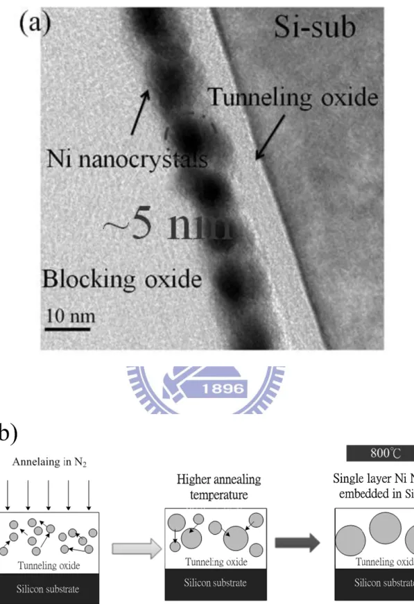
Fig. 3-2 (a) demonstrate the cross-section TEM image of the mixed film after
700℃ RTA process. The double-stacked Ni NC about 5nm were nucleated between
the tunneling oxide and blocking oxide randomly. The distribution of the NC is as
similar as the reported literatures of the NC structure formed by the implantation
[3.9-3.11]. In addition, C-V measurement has also been used to study the
charge-storage ability of the Ni NC. Fig. 3-2 (b) is the C-V curves for the
double-stacked Ni NC memory device. The bidirectional C-V sweeps were performed
from deep inversion to deep accumulation and in reverse, which exhibited a △VFB,
indicating charge-storage ability of the NC. The NC memory device shows an
excellent memory window of 8V under ± 10V gate voltage operations. The excellent
memory window is attributed to the high density NC distribution.
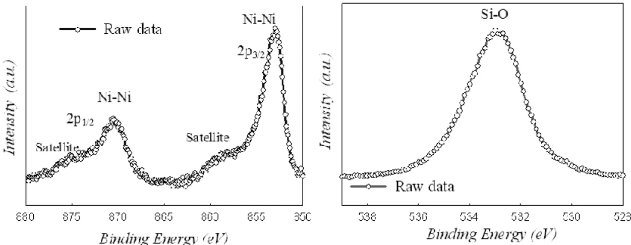
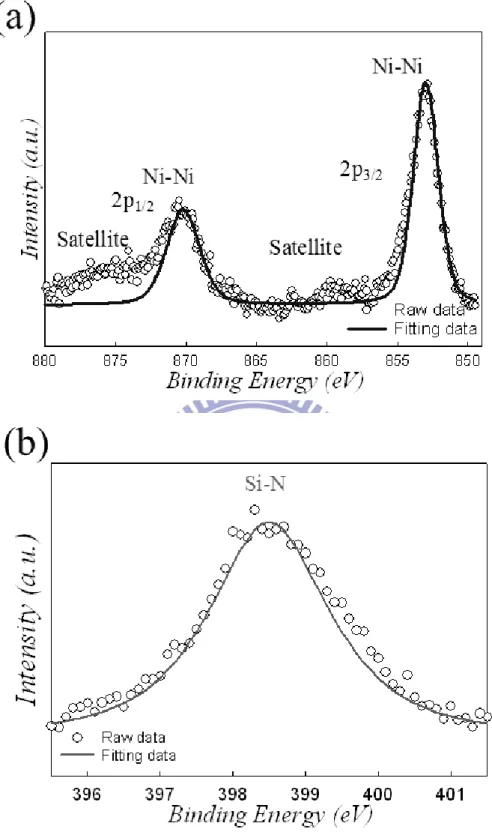
The XPS analysis of the charge-trapping layer with 700℃ annealing condition
has been proposed to study the composition of the charge-trapping layer further. In
Fig. 3-3 (a) and (b), Ni-Ni peak at about 853eV and Si-O peak at about 103eV were
37
the formed structure is the Ni NC embedded in the SiO2 dielectrics layer, which can
provide a good memory window for the device application. Then, we also propose the
forming process of the double-stacked Ni NC as shown as the Fig. 3-3 (c). During the
co-deposition process, nucleation sites for the Ni NC are distributed over the mixed
film randomly. With the external energy is a provided, thermal-driving Ni atom tends
to diffuse and aggregate to form the NC structure due to the surface energy and the
interface stress [3.13]. The Ni NC nucleates randomly in the trapping layer for the
nucleation sites distribution. Hence, the 700℃ annealing temperature though causes
the Ni aggregate but in a random distribution.
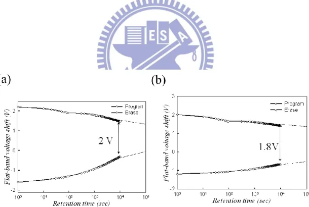
Retention and endurance tests were used to study the reliability behavior of the
Ni NC memory device. The retention measurement was performed at room
temperature by operating a ± 10V gate voltage stress for 10sec and measured up to
104 sec. The memory device keeps about 0.76V at 104sec as shown as the Fig. 3-4 (a). The memory devices show an excellent memory window but a poorer retention
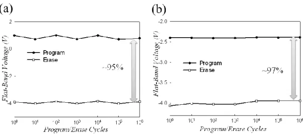
characteristic. In the endurance test, a continuous pulse with ± 10V of gate voltage for
1msec was used to stress the samples. After the stress, a followed C-V measurement
was used to observe the variation of the charge-storage ability. As shown as the results
in the Fig. 3-4 (b), a negligible decay of memory window is found, which is attributed
38
To enhance the retention characteristic of the memory device, a higher annealing
temperature (800℃ for 1min) has been used. However, it is found that the double-
stacked Ni NC transfers to single layer structure after the annealing as shown as the
TEM result of Fig. 3-5 (a). Also, the reasonable forming process for the single layer
Ni NC has also been proposed as shown as the Fig. 3-5 (b). According the reported
literature, the NC formation is affected by the annealing temperature strongly [3.14].
The Ni atoms obtained more driving force to move as the thermal temperature
increasing to 800℃. It causes that the larger size and lower density of NC aggregated
on the tunneling oxide. From the C-V result as shown as the Fig. 3-6, the device
provides a 4V memory window under ± 10V gate voltage sweep. The degenerated
memory window is due to that the single layer with lower NC density.
Fig. 3-7 (a) and (b) is the retention and endurance characteristics of the
single-layer Ni NC memory device, respectively. It can be found that an obvious
improvement of memory window (~2.3V) at 104sec in the single-layer Ni NC memory. The device shows a similar endurance characteristic with the 700 ℃
annealed- one due to the same tunneling oxide forming process. To explain the
improvement of retention behavior, a J-V characteristic has been proposed to study
the leakage current behavior of the devices. As shown as the Fig. 3-8, it can be found
39
magnitude smaller than the sample with 700 ℃ RTA treatment. Based on the
tunneling and blocking oxide of the devices are formed by the similar process, it can
be inferred that the 700℃- sample have additional leakage paths. The additional
leakage paths come from the trap of the interface at the charge-trapping layer and the
surrounding oxide between NC. The traps cause the current is easier to pass through
the capacitor structure during the J-V measurement. A higher temperature during the
NC formation can improve the dielectrics layer. Therefore, the device formed by the
800℃ RTA process can keep more charge in the retention test.
3.1.4 Conclusion
In conclusion, we have demonstrated a co-evaporated method to fabricate the Ni
NC structures successfully. It is found that the diffuse of Ni NC at different annealing
temperature is thought as the major parameter to cause the different Ni NC structures.
We also fabricated the Ni NC memory device to study the memory effect further.
Excellent charge-storage ability is found based on the higher density of
double-stacked Ni NC. However, the device has a poor retention due to the additional
defects provided by the oxide interface. A higher temperature formation process is
confirmed to reduce the device leakage paths. The devices formed by annealing at 800 ℃ shows an excellent charge-storage ability characteristic in the retention test.
40
3.2 High density Ni nanocrystal formed by co-evaporating Ni and
SiO
2pellets for the nonvolatile memory device application
3.2.1 Introduction
In this work, we propose a method to fabricate Ni NC structure by
co-evaporating Ni and SiO2 pellets, simultaneously. An 800℃ RTA was used to
enhance the Ni NC to aggregate. Transmission electron microscope indicates the
formed Ni NC show a high density distribution about 4.5×1012cm-2. Then, the memory device using the Ni NC as charge-trapping centers was fabricated. The Ni
NC memory device has an obvious memory window under capacitance-voltage
measurement. XPS confirms the memory effect results from the Ni NC embedded in
SiO2 dielectric layer. Moreover, related reliability characteristics have also been
extracted.
3.2.2 Experiment
The memory structure was fabricated on a 6 in. p-type Si substrate. First, a
5-nm-thick SiO2 was grown as the tunneling oxide by dry oxidation in atmospheric
pressure chemical vapor deposition furnace. Then, a dual E-gun system was used to
deposit the charge-trapping layer of the device. In the co-deposition process, Ni and
SiO2 pellets were placed in the respective crucible. Subsequently, an about
10-nm-thick mixed film composed of Ni and SiO2 was deposited by co-evaporating
![Fig. 1-6 Schematic illustration of the driving forces in the self-assembly process [1.23]](https://thumb-ap.123doks.com/thumbv2/9libinfo/8412014.179891/33.892.153.743.118.499/fig-schematic-illustration-driving-forces-self-assembly-process.webp)