國 立 交 通 大 學
電子工程學系 電子研究所碩士班
碩 士 論 文
脈衝雷射沉積鑭鋁氧電阻層
全透式電阻式記憶體研究
Pulse-laser deposition of LaAlO
3as resistive switching layer
of fully transparent resistive random access memory
研 究 生:黃 俊 傑
指導教授:張 國 明 博士
脈衝雷射沉積鑭鋁氧電阻層
全透式電阻式記憶體研究
Pulse-laser deposition of LaAlO
3as resistive switching layer
of fully transparent resistive random access memory
研 究 生:黃俊傑 Student:Jun-Jie Huang
指導教授:張國明 博士 Advisor:Dr. Kow-Ming Chang
國 立 交 通 大 學
電子工程學系 電子研究所碩士班
碩 士 論 文
A Thesis
Submitted to Department of Electronics Engineering and Institute of Electronics
College of Electrical and Computer Engineering National Chiao Tung University
in Partial Fulfillment of the Requirements for the Degree of Master in
Electronics Engineering
August 2010
Hsinchu, Taiwan
脈衝雷射沉積鑭鋁氧電阻層
全透式電阻式記憶體研究
學生: 黃俊傑 指導教授: 張國明 博士 國立交通大學 電子工程學系 電子研究所碩士班 摘 要 隨著數位科技的日新月異,非揮發性記憶體在生活中扮演著極 重要的角色,透明化產品也逐漸掀起潮流。快閃式記憶體雖然是目前 最大宗的非揮發性記憶體,但它有其不可微縮的極限,包含高操作電 壓,低存取速度和較短的保存時限。電阻式記憶體具有簡單結構,低 操作電壓和高微縮能力的優點,故很可能成為下一個世代的記憶體。 三氧化鋁鑭為下個世代互補式金屬氧化物半導體的熱門高介電 質材料。三氧化鋁鑭具有高介電常數、不容易與矽反應、在製程中有 低的擴散率且不會在介面和矽產生二氧化矽而造成介電常數等效下 降等優點。如果能利用三氧化鋁鑭作為電阻式記憶體的材料,將很容 易跟互補式金屬氧化物半導體製程相容。 在本論文中,我們成功使用 ITO/三氧化鋁鑭/ITO 製程結構和材Pulse-laser deposition of LaAlO
3as resistive switching layer
of fully transparent resistive random access memory
Student: Jun-Jie Huang Advisor: Dr. Kow-Ming Chang
Department of Electronics Engineering and Institute of Electronics National Chiao Tung University, Hsinchu, Taiwan
ABSTRACT
With the arrival of Digital Age, nonvolatile memory (NVM) plays an important role in our life, and the transparent products are also a trend. The flash memory is the mainstream NVM so far, but it meets the challenge for scaling down, including high operation voltage, low operation speed, and poor retention. Resistive random access memory (RRAM) has many advantages including simple structure, low operation voltage, and scaling down. RRAM is possible to become the next generation NVM.
LaAlO3 is a candidate high k material for next COMS generation.
LaAlO3 is a promising material due to its higher k, lack of reactivity with
Si, and larger band offset with Si. Particularly, LaAlO3 has much lower
atomic diffusion rate and fewer tendencies to form the SiO2-based
interfacial layer during processing. If we can use LaAlO3 as a next
誌 謝
經過這兩年的碩士班學習,不僅讓我學到研究的方法,也讓我更 加了解自己對元件物理領域的興趣。首先感謝 張國明教授在這兩年 的指導並提供舒適的學習環境。也感謝長庚大學 劉國辰教授在實驗 方面的提供和討論,激發了我多元的想法與敏銳的思考。 其次感謝曾文賢學長,在研究過程中不斷的指導和討論。也感謝 長庚的學弟蕭煌錡在實驗過程中不斷的幫忙,讓實驗過程進行得更順 利。感謝實驗室的同學和學弟,在碩士班這兩年帶來歡笑和鼓勵,讓 我在做實驗的時候解決很多問題,進而完成論文。 此外,感謝國家奈米元件實驗室 (NDL) 與交通大學奈米中心 (NCTU – NFC) 的服務人員以及曾經訓練我機台的學長姐和工程 師,因為有你們熱心的幫忙和服務,才能讓我順利進行實驗。 最後,感謝我的家人和女友錢乃瑜,在我挫折的時後給予支持, 在我開心的時候分享喜悅,也因為你們,我才能全心全力在課業上努 力,謝謝你們。Contents
摘 要 ii
ABSTRACT iii
Table Contents vii
Figure Contents vii
Chapter1 Introduction 1
1.1 Introduction to nonvolatile memory 1
1.2 Introduction to resistive random access memory 3
1.3 Conduction mechanisms 3
1.4 Resistive switching mechanisms 6
Chapter 2 Experimental Detail 16
2.1 DC magnetron sputtering system 16
2.2 Pulse Laser Deposition (PLD) system 17
2.3 Fabrication of resistive switching memory device 21
2.4 Material analysis 22
2.5 Electrical analysis 25
Chapter 3 Result and Discussion of Investigation of LaAlO3 Thin
Film with Various Oxygen Pressures 30
3.1 Introduction 30
3.2 Electrical characterization 30
3.3 Physical Characterization 31
Chapter 4 Results and Discussion of the LaAlO3 as a Resistive
Switching Layer in RRAM 49
with different oxygen pressure 50
4.3 Two pads test to detect the rupture position of the filament 53
4.4 Proposed resistive switching mechanisms for ITO/LAO/ITO
structure 54
Chapter 5 Conclusion 81
Chapter 6 Future Work 82
Table Contents
Table 3- 1 ... 33
Figure Contents Fig. 1- 1 Flash memory cell structure [1] ... 11
Fig. 1- 2 The polarization hysteresis curve of the ferroelectric material .. 11
Fig. 1- 3 Valence change systems [1] ... 12
Fig. 1- 4 Evidences for the filament model by CAFM [8] ... 12
Fig. 1- 5 Evidences for the filament model by CAFM [9] ... 13
Fig. 1- 6 Schematic for charge trapping and detrapping I-V curve [10] .. 13
Fig. 1- 7 Schematic for phase change mechanism ... 14
Fig. 1- 8 Schematic for electrochemical metallization mechanism [10] .. 14
Fig. 1- 9 Schematic for schottky barrier mechanism [12] ... 15
Fig. 2- 1 Magnetron sputtering system ... 27
Fig. 2- 2 PLD deposition system ... 27
Fig. 2- 3 Process flow of the MIM structure ... 28
Fig. 2- 4 Atomic Force Microscopy ... 29
Fig. 2- 5 Scanning electron microscopy system ... 29
Fig. 3- 1 Leakage current of LAO films deposited under various oxygen pressures ... 33
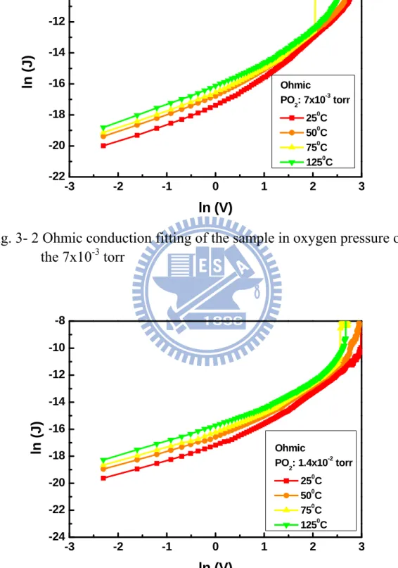
Fig. 3- 2 Ohmic conduction fitting of the sample in oxygen pressure of the 7x10⁻³ torr ... 34
Fig. 3- 4 Ohmic conduction fitting of the sample in oxygen pressure of the 2.8x10⁻² torr ... 35 Fig. 3- 5 Schottky conduction fitting of the sample in oxygen pressure of
the 7x10⁻³ torr ... 35 Fig. 3- 6 Schottky conduction fitting of the sample in oxygen pressure of
the 1.4x10⁻² torr ... 36 Fig. 3- 7 Schottky conduction fitting of the sample in oxygen pressure of
the 2.8x10⁻² torr ... 36 Fig. 3- 8 Breakdown negative voltage with three samples with various
oxygen pressures ... 37 Fig. 3- 9 Breakdown positive voltage with three samples with various
oxygens ... 37 Fig. 3- 10 Breakdown voltage of the sample with oxygen pressure of
7x10⁻³ torr in various temperatures ... 38 Fig. 3- 11 Breakdown voltage of the sample with oxygen pressure of
1.4x10⁻² torr in various temperatures ... 38 Fig. 3- 12 Breakdown voltage of the sample with oxygen pressure of
2.8x10⁻² torr in various temperature ... 39 Fig. 3- 13 Power to breakdown voltage of the sample with oxygen
pressure of 7x10⁻³ torr in various temperatures ... 39 Fig. 3- 14Power to breakdown voltage of the sample with oxygen
pressure of 1.4x10⁻² torr in various temperatures ... 40 Fig. 3- 15 Power to breakdown voltage of the sample with oxygen
pressure of 2.8x10⁻² torr in various ... 40 Fig. 3- 16 AFM of the sample with oxygen pressure of 7x10⁻³ torr ... 41
Fig. 3- 18 AFM of the sample with oxygen pressure of 1.4x10⁻² torr ... 42
Fig. 3- 19 SEM of the sample with oxygen pressure of 7x10⁻³ torr ... 42
Fig. 3- 20 SEM of the sample with oxygen pressure of 1.4x10⁻² torr ... 43
Fig. 3- 21 SEM of the sample with oxygen pressure of 2.8x10⁻² torr ... 43
Fig. 3- 22 XRD of the samples with different oxygen pressure ... 44
Fig. 3- 23 XPS result of La 3d peak with different oxygen pressure ... 44
Fig. 3- 24 XPS result of La 3d peak with different oxygen pressure ... 45
Fig. 3- 25 XPS result of La 3d peak with different oxygen pressure ... 45
Fig. 3- 26 TEM of the sample with oxygen pressure of 7x10⁻³ torr ... 47
Fig. 3- 27 TEM of the sample with oxygen pressure of 1.4x10⁻² torr ... 47
Fig. 3- 28 TEM of the sample with oxygen pressure of 2.8x10⁻² torr ... 48
Fig. 4- 1 Forming process ... 56
Fig. 4- 2 Operation process of the RRAM ... 56
Fig. 4- 3 Heat effect in the larger Icc ... 57
Fig. 4- 4 Relation between the reset voltage and the current in the LAO thin film with oxygen pressure of 7x10⁻³ torr ... 57
Fig. 4- 5 Relation between the reset voltage and the current in the LAO Thin film with oxygen pressure of 1.4x10⁻² torr ... 58
Fig. 4- 6 Relation between the reset voltage and the current in the LAO Thin film with oxygen pressure of 2.8x10⁻² torr ... 58
Fig. 4- 7 Detail of the reset current from different magnitude of the reset voltage in LAO thin film with oxygen pressure of 7x10⁻³ torr ... 59 Fig. 4- 8 Detail of the reset current from different magnitude of the reset
voltage in LAO thin film with oxygen pressure of 2.8x10⁻² torr 60 Fig. 4- 10 Relation of the HRS and the different magnitude of the reset
voltage in LAO thin film with oxygen pressure of 7x10⁻³ torr ... 60 Fig. 4- 11 Relation of the HRS and the different magnitude of the reset
voltage in LAO thin film with oxygen pressure of 1.4x10⁻² torr 61 Fig. 4- 12 Relation of the HRS and the different magnitude of the reset
voltage in LAO thin film with oxygen pressure of 2.8x10⁻² torr 61 Fig. 4- 13 Relation between the negative voltage and the current in the
LAO thin film with oxygen pressure of 7x10⁻³ torr ... 62 Fig. 4- 14 Relation between the negative voltage and the current in the
LAO thin film with oxygen pressure of 1.4x10⁻² torr ... 62 Fig. 4- 15 Relation between the negative voltage and the current in the
LAO thin film with oxygen pressure of 2.8x10⁻² torr ... 63 Fig. 4- 16 Detail of the set current from different magnitude of the
negative voltage in LAO thin film with oxygen pressure of
7x10⁻³ torr ... 63 Fig. 4- 17 Detail of the set current from different magnitude of the
negative voltage in LAO thin film with oxygen pressure of
1.4x10⁻² torr ... 64 Fig. 4- 18 Detail of the set current from different magnitude of the
negative voltage in LAO thin film with oxygen pressure of
2.8x10⁻² torr ... 64 Fig. 4- 19 Relation of the LRS and the different magnitude of the
negative voltage in LAO thin film with oxygen pressure of
negative voltage in LAO thin film with oxygen pressure of
1.4x10⁻² torr ... 65 Fig. 4- 21 Relation of the LRS and the different magnitude of the
negative voltage in LAO thin film with oxygen pressure of
2.8x10⁻² torr ... 66 Fig. 4- 22 Relation of the LRS and the different magnitude of the
compliance current in LAO thin film with oxygen pressure of 7x10⁻³ torr ... 66 Fig. 4- 23 Relation of the LRS and the different magnitude of the
compliance current in LAO film with oxygen pressure of
1.4x10⁻² torr ... 67 Fig. 4- 24 Relation of the LRS and the different magnitude of the
compliance current in LAO film with oxygen pressure of
2.8x10⁻² torr ... 67 Fig. 4- 25 Endurance of the ITO/LAO/ITO sample with oxygen pressure
of 7x10⁻³ torr ... 68 Fig. 4- 26 Endurance of the ITO/LAO/ITO sample with oxygen pressure
of 1.4x10⁻² torr ... 68 Fig. 4- 27 Endurance of the ITO/LAO/ITO sample with oxygen pressure
of 2.8x10⁻² torr ... 69 Fig. 4- 28 Eetention of the ITO/LAO/ITO sample with oxygen pressure
of 7x10⁻³ torr ... 69 Fig. 4- 29 Eetention of the ITO/LAO/ITO sample with oxygen pressure
Fig. 4- 31 Vset/Vreset distribution of the sample with oxygen pressure of 7x10⁻³ torr ... 71 Fig. 4- 33 Vset/Vreset distribution of the sample with oxygen pressure of
2.8x10⁻² torr ... 72 Fig. 4- 34 Relation between the HRS and the temperature show
semiconductor-like behavior ... 72 Fig. 4- 35 Frenkel Poole behavior of the HRS ... 73 Fig. 4- 36 Relation between the HRS and the temperature show metallic
behavior ... 73 Fig. 4- 37 Ohmic behavior of the LRS ... 74 Fig. 4- 38 Schematic diagram of a cross section of the sample structure
for the I-V measurement of the ITO/LAO/ITO/LAO/ITO sample ... 74 Fig. 4- 39 Abnormal forming of the two pads test ... 75 Fig. 4- 40 Resistances change of the different configuration after
abnormal forming of the two pads test ... 75 Fig. 4- 41 Resistances change of the different configuration After the
subsequent reset and set processes of the two pads test ... 76 Fig. 4- 42 Pristine state of the ITO/LAO/ITO structure ... 76 Fig. 4- 43 E-Field generated from the external bias lead to oxygen
migration ... 77 Fig. 4- 44 Oxygen migrate from the cathode to the anode ... 77 Fig. 4- 45 More vacancies migrate from the anode to the cathode ... 78 Fig. 4- 46 Regions near the anode and the cathode show different polarity
oxygen from the cathode the to the anode ... 79 Fig. 4- 48 HRS after the reset operation ... 79 Fig. 4- 49 E-Field makes the oxygen migration from the virtual cathode
to the anode ... 80 Fig. 4- 50 LRS after the set operation ... 80
Chapter1 Introduction
1.1 Introduction to nonvolatile memory
With the popularity of various portable electronics, nonvolatile memories play an important role in our life. An ideal nonvolatile memory has the following advantages: low operation voltage, high operation speed, high endurance, long retention time, and simple structure. There are many kinds of advanced nonvolatile memories, but no one can meet all requests.
1.1.1 Flash
The Flash memory is the mainstream nonvolatile memory, including NOR and NAND flash. The primary structure of the flash memory is a MOSFET-like transistor with an inner floating gate as shown in Fig 1-1. The data stored in the floating gate is by the current charges. When charge stored in the floating gate, it changes the threshold voltage (Vt) of the cell, so the modified Vt causes the cell to be on or off region.
NOR and NAND flash are different from their properties and applications. NOR flash has the advantage for high speed, so it is suitable for the mobile electronics. NAND flash has the advantage for high density, so it is suitable for the large date storage.
With the trend for scaling down the cell size, flash memories meet the challenge due to high operation voltage, low operation speed, and poor retention time. There are many advanced nonvolatile memories to become the next generation memories including ferroelectric random
(MRAM), and Resistive random access memory (RRAM).
1.1.2 MRAM
The magnetic random access memory (MRAM) is also an advanced nonvolatile memory. The data stored in the magnetic material is not by the charges but by the magnetic storage elements. The basic MRAM cell consists of two magnetic layers sandwiching a thin tunneling layer. One of the two magnetic layers is a permanent magnet. By applying external field, the other’s field will be changed. To read data, a small nondestructive voltage is applied to recognize the resistance state.
1.1.3 FeRAM
Ferroelectric random access memory (FeRAM) is possible being next generation nonvolatile memory. A ferroelectric material has two type polarizations. The dielectric constant of a ferroelectric is typically much higher than that of a linear dielectric because of the effects of semi-permanent electric dipoles formed in the crystal structure of the ferroelectric material. When an external bias is applied across the ferroelectric material, the dipoles can be aligned with the external bias. By changing the dipoles direction, we can store “0” or “1” information in the material.
The polarization hysteresis curve of the ferroelectric material is shown in
the next generation nonvolatile memory devices. The details of the RRAM are discussed in next section.
1.2 Introduction to resistive random access memory
Resistive random access memory (RRAM) is one of the most promising candidates for next generation storage applications because of its nonvolatility, simple structure, great scalability potential, and compatibility with current complementary metal oxide semiconductor technology.
1.3 Conduction mechanisms
RRAM has been research for a period of time, but the mechanism of the resistive switching (RS) is not carrier up to now. The theories to explain RS character are conduction mechanisms. The conduction mechanisms mostly involved are Schottky emission, Frenkel-Poole emission, Tunnel or Field emission, Space-charge-limited-current, Ohmic conduction, and Ionic conduction. The six basic conduction mechanisms in insulator are summarized in Table1-1.
1.3.1 Schottky emission
The Schottky emission is caused by thermionic emission of carriers across the barrier height of the interfaces, and through the dielectric film. Temperature is the key factor that energetic carriers can jump across the barrier easily. If the carrier conduct in this mechanism, the plot of ln︱
J/T2︱ versus 1/T in a specific voltage is a straight line, and the slop can be used to determine the permittivity of the insulator. The formula of Schottky emission is expressed as below:
kT
d
qV
q
T
A
J
* 2exp
b/
4
r
0where A* denotes Richardson constant, Φb is the Schottky barrier height,
ε0 is the permittivity of free space, εr is the dynamic dielectric constant, V
is the external applied voltage and d is the insulator thickness.
1.3.2 Frenkel-Poole emission
The Frenkel-Poole (F-P) emission is caused by field-enhanced carrier hopping by defect states in the dielectric material, and the barrier lowering is twice as large as that in Schoottky emission mechanism. If the carrier conduct in this mechanism, the plot of ln︱J︱ versus 1/T in a specific voltage and ln︱J/V︱ versus V1/2 at a specific temperature are straight lines. The formula of F-P emission is expressed as below:
kT
d
qV
q
BV
J
exp
t/
4
r
0
external applied voltage and d is the insulator thickness.
1.3.3 Tunnel or field emission
The tunnel or field emission is caused by carriers through the barrier. Voltage is the key factor that carrier can conduct through the barrier easily. If carrier conduct in this mechanism, the plot of ln︱J/V2︱ versus 1/V is a straight line.
1.3.4 Space-charge-limited current
The theory of space-charge-limited current (SCLC) was first given by Mott and Gurney (1940) and has been extended by many authors. This mechanism is attributed to defects in the dielectric. Trap states is the key factor that carrier can conduct in different degrees. The formula of SCLC is expressed as below: 0 3 2 0
8
9
L
V
J
rWhere μ is the free carrier mobility, εr is the dielectric constant of the material, V is the external applied voltage, L is the insulator thickness, and θ is the ratio of free electrons to trapped electrons.
1.3.5 Ohmic conduction
The Ohmic conduction is caused by thermionic carriers. It happened when the injected carrier is far less than the thermionic carriers. Temperature is another effect in this mechanism. The plot of ln︱J︱
versus ln︱V︱ at fixed temperature and ln︱J︱ verusus 1/T in a specific voltage are straight lines. The formula of Ohmic conduction is expressed as below:
)
exp(
T
c
aV
J
Where a and c denote constants, V is the external voltage, and T is the absolute temperature.
1.4 Resistive switching mechanisms
1.4.1 Oxygen movement mechanism
In many transition metal oxides, oxygen ions defect are much more mobile than cations.
When low voltage is applied on the electrode, the line of I-V plot is straight according to ohmic principle. If larger voltage is applied, the line will not obey the ohmic conduction due to large change of oxygen concentration dramatically.
When larger bias is applied, oxygen ions drift toward the anode, causing the region near the anode become p-conductivity, and the region near the cathode become n-conductivity. The set of mass action equations leads to a strong depletion of the oxygen vacancy concentration in a somewhat larger anodic region. In this situation, the large region of n-conductivity is called “virtual cathode”. This “virtual cathode” moves towards the anode and will finally form a conductive path. When the
electroforming is completed, the bipolar resistance switching (BRS) takes place between the virtual cathode and the anode when reverse external bias is applied.
This redox mechanism has recently been confirmed in detail
[2][3][4].
The plot presented this mechanism is shown in Fig 1-3[2].
1.4.2 Filament model
So far, the resistive switching mechanism is believed because of the formation and rupture of the conducting filaments. This model has been proposed since 1970’s. The most obvious evidences for the filament model are electron-beam-induced current model and C-AFM, as shown in
Fig 1-4[8] and Fig 1-5[9].
When voltage sweep was applied on the anode, the carrier injected from the anode. The carriers diffuse into the oxide and grow toward the cathode, and many branches form, which may have a common base at the anode interface. When one of the branches gets to the anode, the resistance of the dielectric decreases dramatically, and the resistance switching to LRS is formed. The conducting path is so called “filament”. Basically, the common base region of the filament is strong, but the branch of the filament is weak. The weakly formed branches of the filament can easily be thermally ruptured after subsequent I-V measurements, resulting in an HRS of the resistance switching.
This filament mechanism has recently been confirmed in detail
1.4.3 Charge trapping and detrapping mode
This RS mechanism is caused by the charge transfer, trapping and detrapping in the insulator. It is widely explained for RS binary oxides and perovskite oxides.
Defects play an important role in this mechanism. When defect states are empty, they can capture the current electrons, leading to low electron concentration and HRS. After all the defect states are filled, the current electrons are free to drift through the oxide, leading to high electron concentration and LRS. Hence, the resistance change is dominated by the bulk defect states.
This charge trapping and detrapping model has recently been confirmed in detail [9].
The plot presented this mechanism is shown in Fig 1-6[9].
1.4.4 Phase change mechanism
The phase change mechanism exhibits two different phases, amorphous and polycrystalline, to store data information. In reset process, a high magnitude current pulse with short tailing edge is applied on the programmable volume of the phase change material. The temperature of the material exceeds the melting point which eliminates the polycrystalline order in the volume. When the reset pulse is terminated, the device quenches to “freeze in” the disordered structural state. This quench time about several nanoseconds is determined by thermal environment of the device and the fall time of the reset pulse. In set
This phase change mechanism has recently been confirmed in detail
[10]-[13].
The plot presented this mechanism is shown in Fig 1-7[13].
1.4.5 Electrochemical metallization mechanism
This mechanism relies on an electrochemically active electrode metal such as Ag and Cu. The drift of the highly mobile cations result in the metallic dendrites which form highly conductive bridges and the system switches to LRS. By applying the reverse bias, the conducting bridge electrochemical dissolute, and the system switches to HRS.
This electrochemical metallization mechanism has recently been confirmed in detail [14] [15].
The plot presented this mechanism is shown in Fig1-8[15].
1.4.6 Schottky barrier modulation mechanism
Schottky barriers formed between oxide and metal electrodes and are different from various materials. For p-type semiconductor, metal with lower work function has higher schottky barriers for holes. For n-type semiconductor, metal with high work function has higher schottky barriers for electrons.
For schottky barrier mechanism, the interface between the oxide and metal plays an important role for resistive switching. When the external bias applied on the metal, electrons were injected into the oxide, and a large amount of electrons are accumulated into the interface states. The net charges in the interface states resulted in a modulation of the
charges, leading to HRS or LRS.
This Schottky barrier modulation mechanism has recently been confirmed in detail [16][17][18][19].
Fig. 1- 1 Flash memory cell structure
Fig. 1- 2 The polarization hysteresis curve of the ferroelectric material [1]
Fig. 1- 3 Valence change systems [2]
Fig. 1- 5 Evidences for the filament model by CAFM [9]
Fig. 1- 7 Schematic for phase change mechanism [13]
Chapter 2 Experimental Detail
2.1 DC magnetron sputtering system
Sputter system is widely used to deposit thin films for study because of its simple equipment structure, good uniformity for films, low cost, and capability for many kinds of films. There are some basic equipments for sputter structure including vacuum system, pressure monitor system, heating system, gas flow control system, and cooling system.
The magnetron sputtering system plot is shown in Fig 2-1.
2.1.1 Vacuum System
Vacuum system includes two basic equipments, such as mechanical pump and cryogenics pump. Before the deposition, the pressure in the chamber has to be vacuumed down to 5x10⁻⁶ torr by two steps. The first step down to 5x10⁻² torr is by the mechanical pump. Before the second step down to 5x10⁻⁶ torr, the mechanical pump is turn off, and then the cryogenics pump works for lowering pressure.
2.1.2 Pressure monitor system
Two gauges are used to detect the pressure in the chamber, basic pressure detect and the ion gauge.
2.1.3 Heating system
2.1.4 Gas flow control system
The gas flow control system is used to control the ratio among different gas ingredients. In this thesis, only Ar is used in the film deposition. The Ar gas is used for plasma generation.
2.1.5 Cooling system
To avoid the thermal damage of the sputter system, cooling system is necessary. All the systems related to the sputter structure are constructed to provide cooling water to maintain the proper working temperature.
2.2 Pulse Laser Deposition (PLD) system
In comparison with other deposition techniques, including chemical vapor deposition (CVD), magnetron sputtering, spray phrolysis, PLD has many advantages:
1. Only a few parameters, such as laser energy density and pulse repetition rate, need to be controlled during the process.
2. The stoichiometry of the target can be retained in the deposited films.
3. The surface of the film is very smooth.
4. Good quality film can be deposited at room temperature due to the high kinetic energies (>1 eV) of atoms and ionized species in the laser-produced plasma.
In spite of many advantages of PLD, there are some disadvantages: 1. Splashing or the particulates deposition on the films.
2. The narrow angular distribution of the ablated species, which is generated by the adiabatic expansion of laser, produced plasma plume and the pitting on the target surface.
These features limit the usefulness of PLD in producing large area uniform thin films, and PLD has not been fully deployed in industry.
The PLD deposition system plot is shown in Fig 2-2.
2.2.1 Mechanisms of PLD
The principle of pulsed laser deposition, in contrast to the simplicity of the system set-up, is a very complex physical phenomenon. It involves all the physical processes of laser-material interaction during the impact of the high-power pulsed radiation on a solid target. It also includes the formation of the plasma plume with high energetic species, the subsequent transfer of the ablated material through the plasma plume onto the heated substrate surface and the final film growth process. Thus PLD generally can be divided into the following four stages:
1. Laser radiation interaction with the target 2. Dynamic of the ablation materials
3. Decomposition of the ablation materials onto the substrate 4. Nucleation and growth of a thin film on the substrate surface
In the first stage, the laser beam is focused onto the surface of the target. At sufficiently high energy density and short pulse duration, all
with stoichiometry as in the target. The instantaneous ablation rate is highly dependent on the fluences of the laser irradiating on the target. The ablation mechanisms involve many complex physical phenomena such as collisional, thermal and electronic excitation, exfoliation and hydrodynamics.
During the second stage the emitted materials tend to move towards the substrate according to the laws of gas-dynamic and show the forward peaking phenomenon [1]. R.K. Singh [2] reported that the spatial thickness varied as a function of cosn, where n>>1. The laser spot size
and the plasma temperature have significant effects on the deposited film uniformity. The target-to-substrate distance is another parameter that governs the angular spread of the ablated materials. Hanabusa [3] also found that a mask placed close to the substrate could reduce the spreading.
The third stage is important to determine the quality of thin film. The ejected high-energy species impinge onto the substrate surface and may induce various type of damage to the substrate. The mechanism of the interaction is illustrated in the following figure. These energetic species sputter some of the surface atoms and a collision region is established between the incident flow and the sputtered atoms. Film grows immediately after this thermalized region (collision region) is formed. The region serves as a source for condensation of particles. When the condensation rate is higher than the rate of particles supplied by the sputtering, thermal equilibrium condition can be reached quickly and film grows on the substrate surface at the expense of the direct flow of the
Nucleation-and-growth of crystalline films depends on many factors such as the density, energy, degree of ionization, and the type of the condensing material, as well as the temperature and the physical-chemical properties of the substrate. The two main thermodynamic parameters for the growth mechanism are the substrate temperature T and the supersaturation m. They can be related by the following equation:
) / ln(R Re kT m
where k is the Boltzmann constant, R is the actual deposition rate, and Re is the equilibrium value at temperature T.
The nucleation process depends on the interfacial energies between the three phases present – substrate, the condensing material and the vapour. The minimum-energy shape of a nucleus is like a cap. The critical size of the nucleus depends on the driving force, i.e. the deposition rate
the substrates, which subsequently grow and coalesce together. As the supersaturation increases, the critical nucleus shrinks until its height reaches an atomic diameter and its shape is that of a two-dimensional layer. For large supersaturation, the layer-by-layer nucleation will happen for incompletely wetted foreign substrates.
2.3 Fabrication of Resistive Switching Memory Device
The structures of the samples are based on ITO/LaAlO3/ITO MIM
devices, but a few differences would be made to do study, including Pd top electrode, and different oxygen process pressures. The fabrication processes would be stated respectively.
2.3.2 Bottom Electrode
We used the commercial ITO/glass as the bottom electrode and substrate. Before we deposited oxide thin film, the ITO/glass has to be clean by the standard cleaning process. The cleaning procedures were as follows:
1. ITO/glass substrate was washed in de-ionized (DI) water and oscillated in an ultrasonic bath for 10 minutes to remove particles 2. ITO/glass substrate was washed with acetone liquor and oscillated in
an ultrasonic bath for 10 minutes to remove the organic residues. 3. Repeat step 1.
4. ITO/glass substrate was washed with isopropyl alcohol liquor and oscillated in an ultrasonic bath for 10 minutes.
2.3.3 LAO
The LaAlO3 was deposited by PLD as the resistive switching layer.
First, we prepared PLD systems for 15 minutes. Lambda physics of excimer laser was furnished by λ=248 nm, pulse duration of 25 ns, repetition rate of 3 Hz, and the laser energy of 500 mJ. We used various oxygen pressures of 7x10⁻³, 1.4x10⁻², and 2.8x10⁻² torr to deposit LAO thin films with thickness of 45 nm.
2.3.4 Top Electrode
After the fabrication of the resistance switching layer, the top electrode was prepared to form the structure of metal/resistive switching layer/metal. We used DC sputter system to deposited ITO as the top electrode. To prevent the interfacial layer between the top electrode and the LAO thin film from sputtering damage, we deposited the ITO in two DC powers.We deposited the ITO at 5 W in 90 minutes, and then at 10W in 70 minutes. Therefore, the device with MIM structure was completed. The area of the top electrode was defined by the shadow mask with 0.02 cm2. The process flow of the MIM structure is shown in Fig 2-3.
2.4 Material Analysis
In this study, we used different equipments to analyze and measure including X-ray diffraction, X-ray photoelectron spectroscopy, atomic force microscopy, scanning electron microscopy, and transmission
2.3.1 X-ray Diffraction
X-ray diffraction is a useful method to determinate the arrangement of atoms in target. The key step in x-ray crystallography is the diffraction of X-rays scattering from the material, and the scattered X-ray photons are measured in the diffraction measurement.
If the atoms are arranged in a periodic type, the diffracted waves will consist of sharp interference maxima with the same symmetry as in the distribution of atoms, and the peak is related to the atomic distance.
Thin film diffraction method is a very important process development.
2.3.2 X-ray Photoelectron Spectroscopy
When the light illuminates the matter, the inner electrons are going to be excited and ionized. The ionized electrons, which close to the surface of the matter have ability to escape into vacuum, named photoelectron, and the phenomenon is called photoelectric effect. Due to the different components and chemical states of the mater, photoelectrons have characteristic kinetic energy, which can be used to identify the composed elements and the chemical states of surface atoms. Then the excitation source is soft x-ray, the photoemission spectroscopy is termed by X-ray photoelectron spectroscopy, which is core level excitation.
2.3.3 Atomic Force Microscopy
square roughness are automatically recorded and calculated by the software. The schematic diagram of the AFM is shown in Fig 2-4.
2.3.4 Scanning Electron Microscopy
Scanning electron microscopy is a useful method to see the surface morphology and the cross section image of the structure. The accelerated electron beam emitted from the cold-cathode electron gum collides with the target, and the secondary electrons from the surface of the target are detected and rendered into a bright SEM image. The schematic diagram of the SEM system is shown in Fig 2-5.
2.3.5 Focus ion beam (FIB)
FIB is used to shape the sample to meet the request of the TEM measurement. The system is different from the SEM system, because FIB systems use a finely focused beam of ions (usually gallium) rather than the beam of electrons.
The gallium (Ga+) primary ion beam hits the sample surface and sputters a small amount of the material, which leaves the surface as either secondary ions (i+ or i-) or neutral atoms (n0). The primary beam also produces secondary electrons (e-). As the primary beam raster on the sample surface, the signal from the sputtered ions or secondary electrons is collected to form an image.
by the condenser lenses. It is necessary for the device to be very thinner, so the electrons can be transparent through the device. The transmitted and forward scattered electrons form a diffraction pattern in the back focus plane and a magnified bright image in the main screen.
2.5 Electrical Analysis
The electrical analysis is measured by Agilent 4156C system controlled by a desktop computer with the Agilent VEE software. During the electrical analyses, the voltage is applied on the top electrode, and then we record the I-V data. We also use the equipment to measure the data retention time and endurance.
2.4.1 Current-Voltage Measurement
The I-V characteristics of the different conditions are performed by Agilent 4156C. Conducting current is detected by applying a sweep voltage in specific range. The conducting mechanisms are different from various materials. From the I-V curve, we can judge the conducting mechanisms, and the on state with the low resistance or off state with the high resistance can be observed easily.
2.4.2 Data Retention Time Measurement
Data retention is an important performance for nonvolatile memory. It is a period of time for the stored information that can be kept without the power supply. For an ideal memory, data retention time is requested to 10 years. The data retention time is measured at room temperature or
higher temperature for thermal acceleration test.
First, we switch the device to specific state, and then small voltage is applied to read the current to calculate the resistance after a specific period. The more time the date stored in the better data retention the device has.
2.4.3 Endurance Measurement
Endurance is an important performance for the memory. The good endurance performance means that the memory can be program and erase for many times.
First, we switch the pristine device from original state to the low resistance state (LRS), and then switch from the low resistance state to the high resistance state (HRS).That we switch from HRS to LRS and then LRS to HRS is 1 cycle. The more cycles we can operate the better endurance the device has.
Fig. 2- 1 Magnetron sputtering system
Step1:
Commercial glass substrate and ITO electrode initial
Step2:
LaAlO3 deposited by pulsed laser deposition
Step3:
ITO electrode deposited by DC sputter. Fig. 2- 3 Process flow of the MIM structure
Fig. 2- 4 Atomic Force Microscopy
Chapter 3
Result and Discussion of
Investigation of LaAlO
3
thin film with
various oxygen pressures
3.1 Introduction
Among the many potential high-k materials, LaAlO3 has recently
attracted much attention because of its many advantages included it higher K, lack of reactivity with Si, larger band offsets with Si. It is known that oxide film deposited by the pulsed laser deposition (PLD) often has oxygen vacancies which plays important role in the electrical performance of the film [20][21]. According to the paper [22][23][24], oxygen vacancies play an important role in the leakage current.
3.2 Electrical characterization
The electrical properties of the LaAlO films were investigate by current-voltage (I-V) of the ITO/LAO/ITO metal-insulation-oxide metal (MIM) capacitor structures.
Electrical properties of LAO films were deposited in different oxygen pressure and characterized by leakage current measurements, Agilent 4156C system. The ITO/LAO/ITO structures were deposited on the commercial glass with different oxygen pressure of 7x10⁻³, 1.4x10⁻² and 2.8x10⁻² torr, respectively. We used MIM structure to test leakage
Fig 3-1 shows the leakage current density of the LAO MIM sample at 1MV/cm. As show in Fig 3-1, the leakage current density of LAO thin films decreases with the decreasing of the oxygen pressure. Based on the structure analysis of the films mentioned herein, it could be concluded that the leakage current decreased because of the reduction of the oxygen vacancies [].
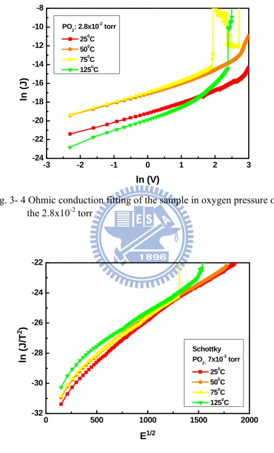
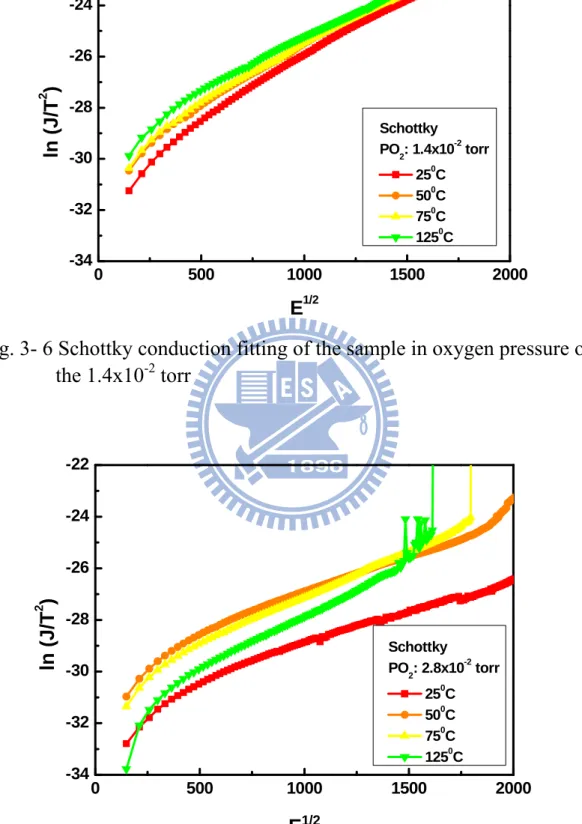
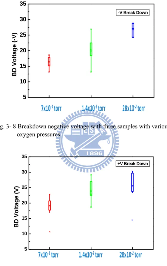
Fig 3-1 shows that the different polarity of the E-Field exhibits different magnitude leakage current. Fig 3-2, Fig 3-3 and Fig 3-4 show the Ohmic conduction fitting of the samples with various oxygen pressures of 7x10⁻³, 1.4x10⁻² and 2.8x10⁻² torr. Fig 3-5, Fig 3-6 and Fig 3-7 show the Schottky conduction fitting of the samples with various oxygen pressures of 7x10⁻³, 1.4x10⁻² and 2.8x10⁻² torr. Fig 3-8 shows the breakdown negative voltages with various oxygen pressures. It shows that the sample with larger oxygen pressure stand larger voltage to breakdown.
Fig 3-9 shows the breakdown positive voltage with various oxygen pressures. It also shows that the sample with larger oxygen pressure stand larger voltage to breakdown.
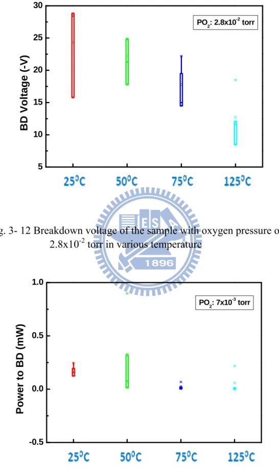
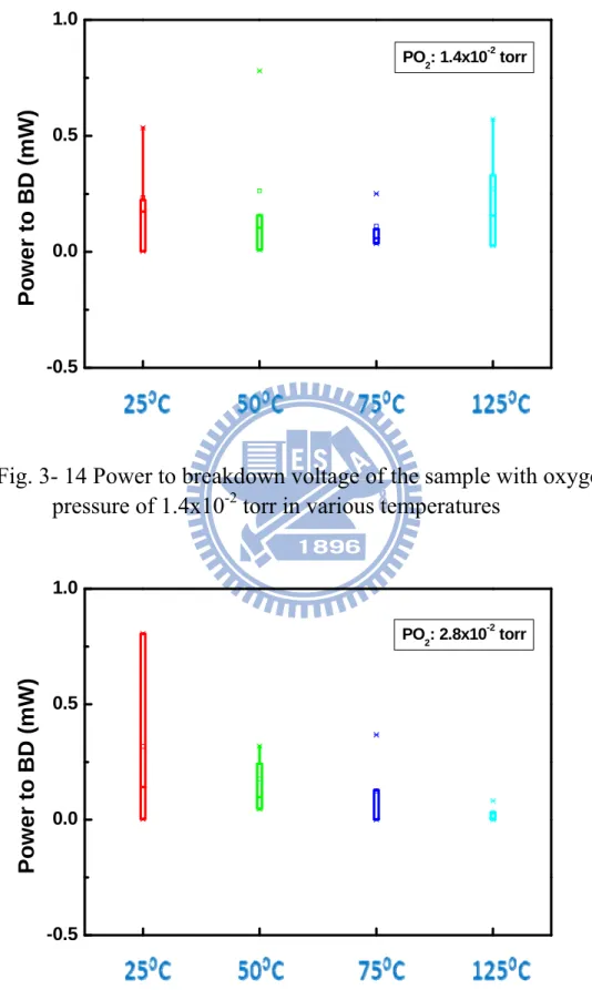
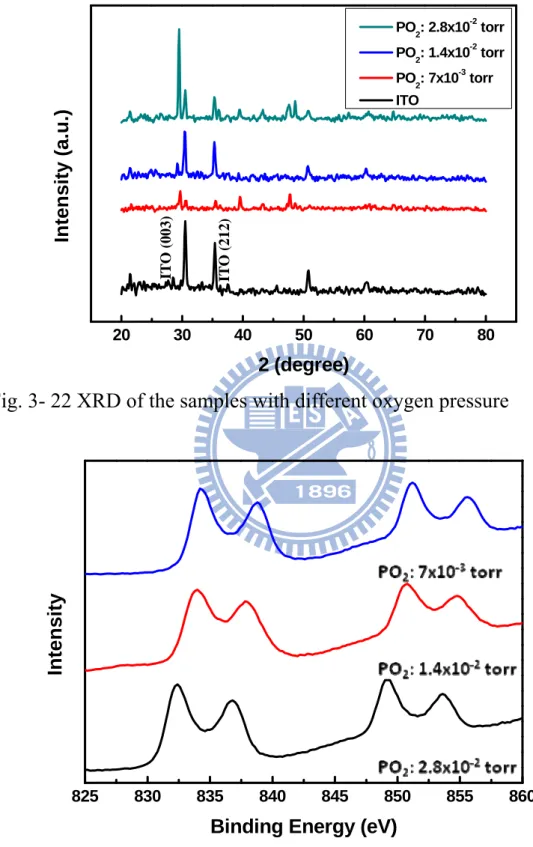
Fig 3-10, Fig 3-11 and Fig 3-12 show that the breakdown voltages of the samples with oxygen pressure in various temperatures. We can find out that the sample with larger phenomenon temperature exhibits lower breakdown voltage. Fig 3-13, Fig 3-14 and Fig 3-15 show that the power to breakdown voltage of the samples in various temperatures. When the temperature is increased, the power to breakdown decreases. This is result from the extra power supplied from the phenomenon.
3.3.1 Atomic force microscope (AFM) and surface roughness analysis Table 3-1 shows the comparison of the surface roughness of the LAO thin films with different oxygen pressure. Fig 3-16, Fig 3-17, and Fig 3-18 show that AFM plot with various oxygen pressure. This may be related to the quality of PLD thin film deposition effects [25] [26].
3.3.2 Scanning Electron Microscopy (SEM) analysis
Fig 3-19, Fig 3-20, and Fig 3-21 show that the surface SEM of the three samples.
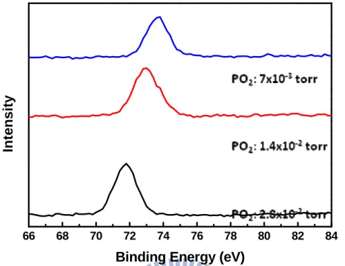
3.3.3 X-ray diffraction (XRD) analysis
Fig 3-22 shows the X-ray diffraction (XRD) analysis of the LAO thin films with different oxygen pressure.
3.3.4 X-ray photoelectron spectroscopy (XPS) analysis
Fig 3-23, Fig 3-24 and Fig 3-25 show that La 3d, Al 2p and O 1s portions of the XPS spectra of LAO thin films. The plots show that the binding energy increases with increasing of the oxygen pressure. However, the low oxygen pressure is favorable to produce large amount of oxygen vacancies [27], and large amount of vacancies result in high leakage current. This is a reliability issue to be concern.
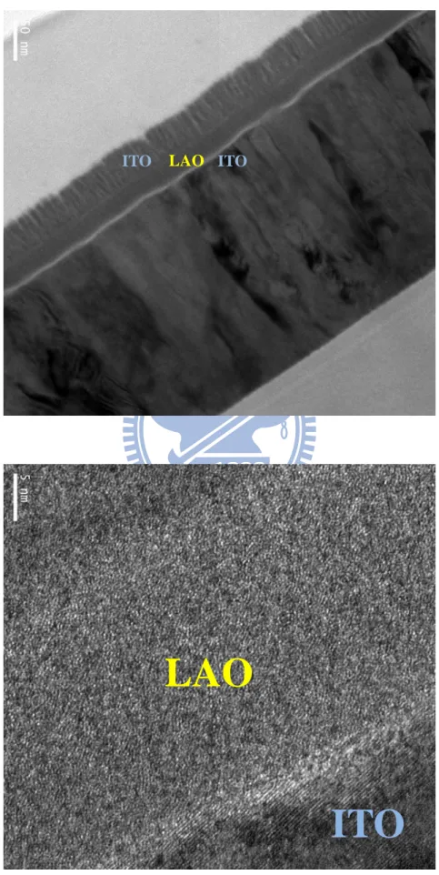
3.3.5 Transmission Electron Microscopy (TEM) analysis
7x10⁻³ torr shows amorphous oxide layer.
Table 3- 1
PO2 7x10
-3
torr 1.4x10⁻² torr 2.8x10⁻² torr Roughness 1.741nm 1.729nm 1.527nm -1.0 -0.8 -0.6 -0.4 -0.2 0.0 0.2 0.4 0.6 0.8 1.0 10-9 10-8 10-7 10-6 10-5 10-4 10-3 10-2 10-1 100 Cu rr en t (m A) E-Field (MV/cm) Leakage Current PO 2: 7x10 -3 torr PO2: 1.4x10⁻² torr PO 2: 2.8x10 -2 torr
Fig. 3- 1 Leakage current of LAO films deposited under various oxygen pressures
-3 -2 -1 0 1 2 3 -22 -20 -18 -16 -14 -12 -10 -8 ln (J) ln (V) Ohmic PO 2: 7x10 -3 torr 250C 500C 750C 1250C
Fig. 3- 2 Ohmic conduction fitting of the sample in oxygen pressure of the 7x10⁻³ torr -3 -2 -1 0 1 2 3 -24 -22 -20 -18 -16 -14 -12 -10 -8 ln ( J) ln (V) Ohmic PO 2: 1.4x10 -2 torr 250C 500C 750C 1250C
-3 -2 -1 0 1 2 3 -24 -22 -20 -18 -16 -14 -12 -10 -8 ln ( J ) ln (V) PO2: 2.8x10⁻² torr 250C 500C 750C 1250C Fig. 3- 4 Ohmic conduction fitting of the sample in oxygen pressure of
the 2.8x10⁻² torr 0 500 1000 1500 2000 -32 -30 -28 -26 -24 -22 ln (J/T 2 ) E1/2 Schottky PO2: 7x10⁻³ torr 250C 500C 750C 1250C Fig. 3- 5 Schottky conduction fitting of the sample in oxygen pressure of
0 500 1000 1500 2000 -34 -32 -30 -28 -26 -24 -22 ln (J/T 2 ) E1/2 Schottky PO 2: 1.4x10 -2 torr 250C 500C 750C 1250C Fig. 3- 6 Schottky conduction fitting of the sample in oxygen pressure of
the 1.4x10⁻² torr 0 500 1000 1500 2000 -34 -32 -30 -28 -26 -24 -22 ln (J /T 2 ) E1/2 Schottky PO2: 2.8x10⁻² torr 250C 500C 750C 1250C Fig. 3- 7 Schottky conduction fitting of the sample in oxygen pressure of
5 10 15 20 25 30 35 BD Vo ltage (-V) -V Break Down Fig. 3- 8 Breakdown negative voltage with three samples with various
oxygen pressures 5 10 15 20 25 30 35 BD Vo ltag e (V) +V Break Down Fig. 3- 9 Breakdown positive voltage with three samples with various oxygen pressures
5 10 15 20 25 30 BD Vo ltag e (-V) PO2: 7x10⁻³ torr Fig. 3- 10 Breakdown voltage of the sample with oxygen pressure of
7x10⁻³ torr in various temperatures
5 10 15 20 25 30 BD Vo lt ag e (-V) PO2: 1.4x10⁻² torr
5 10 15 20 25 30 BD Vo lt ag e (-V) PO2: 2.8x10⁻² torr
Fig. 3- 12 Breakdown voltage of the sample with oxygen pressure of 2.8x10⁻² torr in various temperature
-0.5 0.0 0.5 1.0 Power to BD ( m W) PO2: 7x10⁻³ torr Fig. 3- 13 Power to breakdown voltage of the sample with oxygen
pressure of 7x10 torr in various temperatures -0.5 0.0 0.5 1.0 Power to B D ( m W) PO2: 1.4x10⁻² torr
Fig. 3- 14 Power to breakdown voltage of the sample with oxygen pressure of 1.4x10⁻² torr in various temperatures
-0.5 0.0 0.5 1.0 Power to BD ( m W) PO 2: 2.8x10 -2 torr
pressure of 2.8x10⁻² torr in various temperatures
Fig. 3- 16 AFM of the sample with oxygen pressure of 7x10⁻³ torr
Fig. 3- 17 AFM of the sample with oxygen pressure of 1.4x10⁻² torr
Fig. 3- 18 AFM of the sample with oxygen pressure of 2.8x10⁻² torr
Fig. 3- 20 SEM of the sample with oxygen pressure of 1.4x10⁻² torr
IT O (00 3 ) IT O (21 2 ) 20 30 40 50 60 70 80 In ten s ity (a. u .) 2 (degree) PO2: 2.8x10⁻² torr PO 2: 1.4x10 -2 torr PO 2: 7x10 -3 torr ITO
Fig. 3- 22 XRD of the samples with different oxygen pressure
825 830 835 840 845 850 855 860
Intensit
y
Binding Energy (eV)
66 68 70 72 74 76 78 80 82 84
Intensit
y
Binding Energy (eV)
Fig. 3- 24 XPS result of Al 2p peak with different oxygen pressure
524 526 528 530 532 534 536 538 540 542
Intensit
y
Binding Energy (eV)
LAO ITO ITO
LAO
Fig. 3- 26 TEM of the sample with oxygen pressure of 7x10⁻³ torr
LAO ITO ITO
LAO
ITO
LAO
ITO ITO
LAO
Chapter 4
Results and Discussion of the LaAlO
3
as
a resistive switching layer in RRAM
4.1 Specified some resistive switching parameters
First, we have to define some switching parameters in our experiment. When a small external voltage is applied on the MIM structure, small current can be detected. The small current is called “leakage current”. The larger external voltage is applied, the larger current flow through the insulator and there will be possible a current increasing abrupt. This is call “forming” process, as shown in Fig 4-1. The forming process is the common phenomenon in the metal oxide films which is similar to the dielectric breakdown, named it “soft breakdown”.
In general, resistive switching material exhibits two memory states: the low resistance state (LRS), also named high conducting state (ON-state) and the high resistance state (HRS), also named low conducting state (OFF-state), which can be altered by applying bias voltage, and utilizes the two different resistance values to storage digital data. The resistance value of high resistance state is defined as HRS (Roff).
The resistance value of low resistance state is defined as LRS (Ron). ON
process is defined as the transformation from LRS into HRS. Reverse process is defined as the Off process. During ON process, a sudden increase in current occurs at VSET and limited at compliance current.
During OFF process, a drop decrease in current occurs at VRESET by dc
The compliance current (Icc) is an important parameter in RRAM switching operation.. If there is no Icc in operation, large current will cause device “hard breakdown”. Proper Icc value is necessary. Lower Icc value cannot cause HRS to LRS, and larger Icc may cause heat effect that make the device switch unstable, as shown in Fig 4-3. In the proper region, the larger Icc value, the lower LRS.
4.2 comparison of switching properties between LAO thin
films with different oxygen pressure
4.2.1 Various magnitude of the positive voltage sweep
Fig 4-4, Fig 4-5 and Fig 4-6 show that the relations between the positive voltage and the current in the LAO thin films with oxygen pressure of 7x10⁻³, 1.4x10⁻² and 2.8x10⁻² torr. Fig 4-7, Fig 4-8 and Fig 4-9
show that the detail of the reset current from different magnitude of the positive voltage in LAO thin films with oxygen pressure of 7x10⁻³, 1.4x10⁻² and 2.8x10⁻² torr. The larger positive voltage is applied, the smaller the reset current conducts through the thin film. We use very small voltage, 0.1 V, to read the resistance after positive voltage is applied.
Fig 4-10, Fig 4-11 and Fig 4-12 show that the relations of the HRS and the different magnitude of the reset voltage in LAO thin film with oxygen pressure of 7x10⁻³, 1.4x10⁻² and 2.8x10⁻² torr. We can find out that when we applied more positive voltage on the top electrode of the ITO/LAO/ITO structure, the resistance becomes larger. There are a
4.2.2 Various magnitudes of the negative voltage sweep
Fig 4-13, Fig 4-14 and Fig 4-15 show that the relations between the negative voltage and the current in the LAO thin films with oxygen pressure of 7x10⁻³, 1.4x10⁻² and 2.8x10⁻² torr. Fig 4-16, Fig 4-17 and Fig 4-18 show that the detail of the set current from different magnitude of the negative voltage in LAO thin films with oxygen pressure of 7x10⁻³, 1.4x10⁻² and 2.8x10⁻² torr. The smaller negative voltage is applied on the top electrode of the ITO/LAO/ITO structure, the larger the set current conduct through the LAO thin film. We applied very small voltage to read the resistance after negative voltage is applied. Fig 4-19, Fig 4-20 and Fig 4-21 show that the relations of the LRS and the different magnitude of the negative voltage in LAO thin film with oxygen pressure of 7x10⁻³, 1.4x10⁻² and 2.8x10⁻² torr. We can find out that when we applied smaller negative voltage on the structure, the set current becomes larger, and the resistance becomes smaller. There are a relationship between the negative E-Field and the resistance.
4.2.3 Various magnitude of the compliance current
Fig 4-22, Fig 4-23 and Fig 4-24 show that the relations between the compliance current and the conducting current in the LAO thin films with oxygen pressure of 7x10⁻³, 1.4x10⁻² and 2.8x10⁻² torr. We can find out that the larger compliance current is restricted, the larger conducting current after set operation. This interesting phenomenon is result from the larger conducting path is formed because of the larger current conducting through the thin film.
4.2.4 Endurance
Fig 4-25, Fig 4-26 and Fig 4-27 show the endurance of the three samples with oxygen pressure of 7x10⁻³, 1.4x10⁻² and 2.8x10⁻² torr. The sample with oxygen pressure of 7x10⁻³ torr exhibited the smallest operation cycles, but the sample with oxygen pressure of 2.8x10⁻² torr exhibited the largest operation cycles. The sample with oxygen pressure of 2.8x10⁻² torr also shows stable resistive switching.
4.4.5 Retention
Fig 4-28, Fig 4-29 and Fig 4-30 show the retention of the tree samples with oxygen pressure of 7x10⁻³, 1.4x10⁻² and 2.8x10⁻² torr. The data retention is at least over 104 seconds.
4.4.6 Vset/Vreset distribution
Fig 4-31, Fig 4-32 and Fig 4-33 show the Vset/Vreset of the sample with different oxygen pressure of 7x10⁻³, 1.4x10⁻² and 2.8x10⁻² torr. The sample with oxygen pressure of 7x10⁻³ torr shows larger distribution of the Vset and Vreset, and the sample with oxygen pressure of 2.8x10⁻² torr show small distribution of the Vset and Vreset.
4.4.7 The conduction behavior of the HRS and LRS
Fig 4-34 and Fig 4-35 show the semi-conduction behavior of the HRS, and the Fig 4-36 and 4-37 show the Ohmic conduction behavior of the LRS. According to the different behavior of the two resistance states
different resistance states.
4.3 Two pads test to detect the rupture position of the
filament
Fig 4-38 shows a schematic diagram of a cross section of the sample structure for the I-V measurement of the ITO/LAO/ITO/LAO/ITO sample. Here, contact 1 and bottom contact 3 (or contact 2 and bottom contact 3) were used to determine the resistance state and operate resistive switching.
Fig 4-39 shows that the current increased dramatically at ~-40V, and then decreased dramatically at ~45V. Fig 4-40 shows that the resistances change of 1-2 and 1-3 configurations before and after the electroforming. It is believed that the resistance of the 1-2 configuration decrease because of the resistances change of the 1-3 and 2-3 configurations. The resistance of the 1-3 configuration increased dramatically because of the high power of the operation. It is coincide that the resistive switching occurs at the anode.
To prevent the operation from the abnormal electroforming, the forming operation is operated separately. To forming the 1-3 configuration, contact 1 was biased negatively with contact B grounded. To forming the 2-3 configuration, contact 2 was biased positively with contact B grounded. The pristine resistances of the 1-2 and 1-3 configurations are about ~ 108 ohm. After the subsequent reset and set processes, Fig 4-41 show that the resistance of the 2-3 configuration changes as a function of the cycle. It is coincided that the resistive
4.4 Proposed resistive switching mechanisms for
ITO/LAO/ITO structure
We proposed a resistive switching mechanism of the ITO/LAO/ITO structure by the oxygen migration model. Fig 4-42 to Fig 4-50 shows the resistive switching mechanism of the ITO/LAO/ITO structure. When the negative bias is applied on the top electrode, an E-Field is generated from the anode to the cathode. The E-Field makes the oxygen ions move from the cathode to the anode. When the larger voltage is applied on the device, the larger E-Field make the oxygen migrate apparently as show in Fig 4-45. The large E-Field leads to a significant increase of the oxygen vacancy concentration near the cathode, and a strong depletion of the oxygen vacancy concentration in a somewhat larger anodic region. The region near the cathode is an n-conductivity, and the region near the anode is a p-conductivity, as show in Fig 4-46. The n-conducting cathodic region is called “virtual cathode”, and it extend toward the anode. If the virtual cathode almost touches the anode, the resistance of the device decreases dramatically. This is called “electroforming”. If the positive bias is applied to the top electrode, the E-Field results in the oxygen migration from the anode to the cathode, and the oxygen recombined with the vacancy near the cathode. The current through oxide decreased dramatically, as show in Fig 4-48, and the off-state is finished. If the negative bias is applied to the top electrode, the E-Field results in the
turning the contact into the on-state, as show in Fig 4-50. Apparently, the oxygen migration by the different polarity of the E-Field between the virtual and the contact constitutes the core process of the bipolar switching.
0 5 10 15 20 25 30 0.0 0.2 0.4 0.6 0.8 1.0 Current ( m A ) Voltage (V) forming
Fig. 4- 1 Forming process
Fig. 4- 3 Heat effect
-4 -3 -2 -1 0 1 2 3 4 5 10-2 10-1 100 101 Cu rr en t (m A) Voltage (V) PO 2:7x10 -2 torr 1 V 1.4V 2 V 2.5V 4 V
Fig. 4- 4 Relation between the reset voltage and the current in the LAO thin film with oxygen pressure of 7x10⁻³ torr
-4 -3 -2 -1 0 1 2 3 4 5 10-2 10-1 100 101 Cu rren t (m A) Voltage (V) PO2:1.4x10⁻² torr 0.6V 1 V 1.4V 2 V 2.5V 3 V
Fig. 4- 5 Relation between the reset voltage and the current in the LAO thin film with oxygen pressure of 1.4x10⁻² torr
-4 -3 -2 -1 0 1 2 3 4 5 10-2 10-1 100 101 Cu rren t (m A) Voltage (V) PO2:2.8x10⁻² torr 0.2V 0.6V 1 V 1.4V 2.5V 3 V
0.00 -0.02 -0.04 -0.06 -0.08 -0.10 -0.12 -0.14 -0.16 0.0 0.1 0.2 0.3 0.4 0.5 Cu rren t (m A) Voltage (V) PO 2:7x10 -3 torr 1 V 1.4V 2 V 2.5V 4 V
Fig. 4- 7 Detail of the reset current from different magnitude of the reset voltage in LAO thin film with oxygen pressure of 7x10⁻³ torr
0.00 -0.02 -0.04 -0.06 -0.08 -0.10 -0.12 -0.14 -0.16 0.0 0.1 0.2 0.3 0.4 0.5 Cu rr en t (m A) Voltage (V) PO2:1.4x10⁻² torr 0.6V 1 V 1.5V 2 V 2.5V 3 V
Fig. 4- 8 Detail of the reset current from different magnitude of the reset voltage in LAO thin film with oxygen pressure of 1.4x10⁻² torr
0.00 -0.02 -0.04 -0.06 -0.08 -0.10 -0.12 -0.14 -0.16 0.0 0.1 0.2 0.3 0.4 0.5 Cu rr en t (m A) Voltage (V) PO 2:28x10 -2 torr 0.2V 0.6V 1 V 1.4V 2.5V 3 V
Fig. 4- 9 Detail of the reset current from different magnitude of the reset voltage in LAO thin film with oxygen pressure of 2.8x10⁻² torr
1.0 1.5 2.0 2.5 3.0 3.5 4.0 101 102 103 104 Resistan ce (o hm) Voltage (V) PO2:7x10⁻³ torr HRS LRS
0.5 1.0 1.5 2.0 2.5 3.0 101 102 103 104 Resistan ce (o h m ) Voltage (V) PO2:1.4x10⁻² torr HRS LRS
Fig. 4- 11 Relation of the HRS and the different magnitude of the reset voltage in LAO thin film with oxygen pressure of 1.4x10⁻² torr
0.0 0.5 1.0 1.5 2.0 2.5 3.0 101 102 103 104 R e sistance (ohm) Voltage (V) PO2:28x10-2 torr HRS LRS
Fig. 4- 12 Relation of the HRS and the different magnitude of the reset voltage in LAO thin film with oxygen pressure of 2.8x10⁻² torr
-10 -8 -6 -4 -2 0 2 10-2 10-1 100 101 Cu rr en t (m A) Voltage (V) PO2:7x10⁻³ torr -10 -5 -3 -1.2 -1 -0.8 -0.5
Fig. 4- 13 Relation between the negative voltage and the current in the LAO thin film with oxygen pressure of 7x10⁻³ torr
-10 -8 -6 -4 -2 0 2 10-2 10-1 100 101 Cu rr en t (m A) Voltage (V) PO 2:1.4x10 -2 torr -10 -5 -3 -2 -1 -0.5 -0.2
-10 -8 -6 -4 -2 0 2 10-2 10-1 100 101 Cu rr en t (m A) Voltage (V) PO2:2.8x10⁻² torr -10 V -5 V -3 V -1.5V -1.2V -1 V -0.8V -0.5V -0.2V
Fig. 4- 15 Relation between the negative voltage and the current in the LAO thin film with oxygen pressure of 2.8x10⁻² torr
0.00 0.02 0.04 0.06 0.08 0.10 0.12 0.14 0.16 0.0 0.1 0.2 0.3 0.4 0.5 Cu rr en t (m A) Voltage (V) PO2:7x10⁻³ torr -10 -5 -3 -1.2 -1 -0.8 -0.5
Fig. 4- 16 Detail of the set current from different magnitude of the negative voltage in LAO thin film with oxygen pressure of 7x10⁻³ torr
0.00 0.02 0.04 0.06 0.08 0.10 0.12 0.14 0.16 0.0 0.1 0.2 0.3 0.4 0.5 Cu rren t (mA) Voltage (V) PO 2:1.4x10 -2 torr -10 V -5 V -3 V -2 V -1 V -0.5V -0.2V
Fig. 4- 17 Detail of the set current from different magnitude of the negative voltage in LAO thin film with oxygen pressure of 1.4x10⁻² torr 0.00 0.02 0.04 0.06 0.08 0.10 0.12 0.14 0.16 0.0 0.1 0.2 0.3 0.4 0.5 Cu rr en t (m A) Voltage (V) PO 2:2.8x10 -2 torr -10 V -5 V -3 V -1.5V -1.2V -1 V -0.8V -0.5V -0.2V
-10 -8 -6 -4 -2 0 102 103 104 Resistance ( ohm) Voltage (V) PO2:7x10⁻³ torr HRS LRS
Fig. 4- 19 Relation of the LRS and the different magnitude of the negative voltage in LAO thin film with oxygen pressure of 7x10⁻³ torr -10 -8 -6 -4 -2 0 102 103 104 R esist ance (ohm) Voltage (V) PO 2:1.4x10 -2 torr HRS LRS
Fig. 4- 20 Relation of the LRS and the different magnitude of the negative voltage in LAO thin film with oxygen pressure of 1.4x10⁻² torr