I
國 立 交 通 大 學
顯示科技研究所碩士班
碩士論文
高開關電流比之高分子垂直電晶體
High on/off current ratio polymer vertical transistor
研 究 生:古明哲
指導教授:冉曉雯 教授
II
高開關電流比之高分子垂直電晶體
High on/off current ratio polymer vertical transistor
研 究 生:古明哲 Student:Ming-Che Ku
指導教授:冉曉雯 教授 Advisor:Prof. Hsiao-Wen Zan
國立交通大學 顯示科技研究所碩士班
碩士論文
A Thesis
Submitted to Display Institute
College of Electrical Engineering and Computer Science National Chiao Tung University
in partial Fulfillment of Requirements for the Degree of Master
in
Display Institute , June 2010
Hsinchu, Taiwan, Republic of China
I
高開關電流比之高分子垂直電晶體
研究生:古明哲
指導教授:冉曉雯 教
授國立交通大學
顯示科技研究所碩士班
Chinese Abstract
中文摘要
有機半導體為近年來學術界積極開發知新穎元件,有機半導體主要訴求為低成本 以及高效率,還有穩定性。在成熟的平面場效電晶體製程下做了許多的改進,但是在 高效率前題下往往需要是極佳的表面性質,也用到了矽基板還有氧化矽等材料,做出 來的效果也往往需要極大的電壓,對於真正的應用有極大的障礙。於是我們採用垂直 的電晶體結構,此結構類似於真空管的運作原理。我們最佳化此結構可以達成甚至超 越同樣材料平面電晶體的開關比,以及更小的操作電壓,更大的輸出電流。這篇提出 了三大類結構,第一個是下方注入的結構,擁有較高的開關比,並且探討了控制閘極 在空間位置上的影響。第二種是上端注入,擁有較好的材料相容性,比較不受 ITO 功 函數限制,相信對於未來空氣穩定材料有相當的助益。第三種基於第一種結構簡化, 利用自我組裝分子來取代部分絕緣層,並使用溶液緩慢乾燥的技術來達成更高的輸出II
電流並抑制控制閘極的漏電。
這篇論文確實提供了垂直空間限制電荷電晶體相當的資訊以及探討,也提出相當 可靠並且簡單的製程。
III
High on/off current ratio polymer vertical transistor
Student:Ming-Che Ku Advisor:Prof. Hsiao-Wen Zan
English Abstract
Display Institute
National Chiao Tung University
Abstract
High performance OTFT has been studied for many years. The most important issue is low cost, high performance, and stability. By the mature process of MOSFET, OTFT has been improved a lot, but unfortunately most of them are fabricated on silicon base or thermal oxide, this is expensive and not suit for low cost requirement. For future application, we fabricated a vertical organic transistor, which is similar to vacuum tube. We achieved a comparable performance of on/off ratio, and lower driving voltage, increasing output current compared to the FET made by same P3HT materials. Here we purposed three kinds of SCLT devices. First is bottom injection SCLT, which owns highest on/off ratio. And then we discussed the impact of grid position in the SCLT space. The second is top injection which is good for new ambient material, because we won’t be limit by ITO work function. Third is simplified from the first structure, we use SAM to replace insulator layer, and use in solvent annealing SCLT devices, which has great output current but higher grid leakage current. By using SAMs treatment, we get higher current gain.
IV
Here we discussed a lot of information and process about SCLT, it’s useful for future developing.
V
Acknowledgements
感謝冉曉雯教授這兩年多的指導,記得當年老師積極的態度讓我印象深刻也讓我 有機會認識有機元件的世界。學生能與老師進行討論,實驗室提供許多資源追求穩定 的進展也有一定的自由可以實踐自己想法,這對於學生來說是探索成長的好環境,而 在與實驗室相互激盪鼓勵的過程更是十分過癮。學海無涯,在當初只是懵懵懂懂的大 學生,感謝宇強、武衛、俊宇、士欽的指導,另外還有帶我入門的鈞銘、淑玲,是你 們鍛鍊我能獨當一面,庭毓、琇玟、世益,許多事情你們幫了我許多。當然還有一起 打拚的夥伴, 海龍、牛哥,沒有你們我們可能永遠都做不出好結果,你們是最可靠的 夥伴。還有學弟妹,王辰、鍾翰、罄合,特別是王辰,你是優質好學弟。另外還有在 交映樓的田伯,和你討論你總是非常有想法,讓我學習不少。還有許多幫忙的朋友同 學們。還有孟心飛老師,精闢的見解往往讓人茅塞頓開。 想起大學時我的指導教授張達文教授儘管得了胃癌,仍然陪我們吃飯,我不能忘 記那時在台大醫院他依然在病床上唸著牛頓的<自然哲學的數學原理>,告訴我們人一 生就應該做一些有趣沒人做過的事。儘管老師你已經不在了,我想你在我們物理 07 級確實種下了小小的幼苗。 感謝我的口試委員,孟心飛老師,陳方中老師,洪勝富老師。 最後是我的家人,很感謝爸媽可以讓我安心的唸完碩班,還有我的女朋友,在許 多艱難時刻陪我走過。 明哲 2010.07.26VI
Contents
CHINESE ABSTRACT I
ENGLISH ABSTRACT III
ACKNOWLEDGEMENT V
CONTENTS VI
FIGURE CAPTIONS VIII
TABLE CAPTIONS XI
CHAPTER 1 INTRODUCTION ... 1
FIGURE OF CHAPTER 1 ... 5
CHAPTER 2 Theorem of oranic devices ... 6
2.1 Chemical structure of SCLT materails... 6
2.2 Charge transport in polymeric semicondutros ... 8
2.3 Metal/poymer/metal schottky diode ... 9
2.3 Space charge limit current ... 10
FIGURE OF CHAPTER 2 ... 13
CHAPTER3 Devices fabrication ... 17
3.1 ITO patterning ... 19
3.2 Material testing-MIM diode and mobility calculation ... 19
3.3 PVP treatment and insulating property ... 20
3.4 Self-assembling monolayer treatment ... 20
FIGURE OF CHAPTER 3 ... 22
CHAPTER4 Result and discussion ... 29
4.1 Discussions that P3HT varies with thickness ... 29
4.2 Grid position discussion ... 29
4.3 Electorde work function difference ... 31
4.4 Band diagram in SCLT ... 32 4.5 SAMs treatment ... 33 FIGURE OF CHAPTER 4 ... 22 CHAPTER4 Conclusion ... 43 Appendix ... 45 Reference ... 46
VII
Figure Captions
FIGURE OF CHAPTER 1 5
1 Schematic device structures ... 5
FIGURE OF CHAPTER 2 ... 13
2-1 Chemical structure of the rr-P3HT ... 13
2-2 (a) Crystallite structure in polythiophenes. (b) Plane-on and (c) edge-on texture of polymeric crystallites... 13
2-3 Chemical structures of the TFB ... 14
2-4 Chemical structures of the PVP and PMF ... 14
2.5 (a) The molecule are structure of polyacetylene (b)Schematic representation of the electronic bonds in polyacetylene ... 15
2-6 band diagram of schottky contact ... 15
2-7 band diagram of ohmic contact ... 15
2-8 The injection charge which can not transport or recombine immediately, and accumulate in the metal-semi interface. ... 16
2-9 Band diagrams of deep traps and shallow traps ... 16
FIGURE OF CHAPTER 3 ... 22
3-1 The name of every layer, reflect to Table ... 22
3-2 Table 1 ... 22
3-3 Process flow of top injection SCLT. ... 23
3-4 Process flow of bottom injection SCLT ... 23
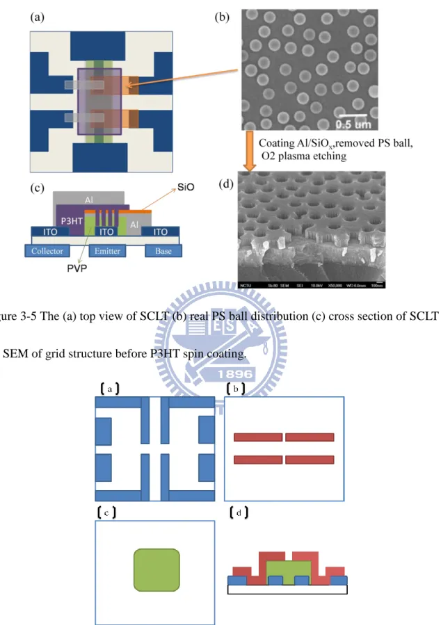
3-5 The (a) top view of SCLT (b) real PS ball distribution (c) cross section of SCLT (d) the SEM of grid structure before P3HT spin coating. ... 24
3-6 The diode of (a) bottom electrode (b) top electrode (c) definition of active area (d) the cross section of diode. ... 24
3-7 A space charge limit diode (ITO/P3HT/Al) (a) log J-V curve (b)and double log J-V curve, the slope=2 means the SCLC region ... 25
3-8 Pure metal-insulator-metal diode result, (a) is PVP with 2000Å , 1500Å , 1000Å (b) is PVP1000Å plus 0Å , 50Å , 100Å , 150Å SiOx ... 26
3-9 Pure MIM(ITO/PVP/Al) diode, PVP with (a)O2 plasma 50W (b) UV-ozone treated before Al electrode deposition ... 27
3-10 (a) Chemical structure of n-octadecylphosphonic acid (b) SAMs treated MIM diode (Al/SAM/Al) insulating property (c) MIM (ITO/SAM/Al) insulating property ... 28
VIII
FIGURE OF CHAPTER 4 ... 35
4-1 Diode structure which is (a) different mobility vary with thickness. Here we can see mobility increase with thickness (b) Different mobility vary with electrical field (c) the voltage of second order value vary with thickness. ... 36
4-2 UV-vis absorption spectrum of different thickness P3HT on ITO ... 36
4-3 Output current of different SCLT vary with grid voltage at similar voltage ... 37
4-4 (Table2) ... 37
4-5 Left is Al as collector, right is ITO as collector. Top emitter SCLTs. ... 38
4-6 A band diagram for (a)grid near to collector and (b) grid near to emitter... 39
4-7 The grid leakage current (a) SAMs treatment and (b) without treatment ... 40
4-8 SCLT with SAMs treatment ... 41
4-9 SCLT without SAMs treatment ... 42
Appendix ... 45 A-1 Various structures simulation results ... 45
IX
Table Captions
Table1 various SCLT details……….………22 Table2 Different SCLT calculating result……….……….37
1
Chapter I
Introduction
Organic thin film transistor (OTFT) has been researched for many years, high driving voltage and low current output is still a serious problem for application. One of the key components is FET, a horizontal device states (on/off ratio) and the field-effect mobility are two parameters to characterize the organic field-effect transistors states (on/off ratio) and the field-effect mobility. So far the organic FET shows low current output because of the intrinsically low carrier mobility due to the weak wave function overlaps between the molecules and the disorder in the thin film. The low mobility also strongly limits the operation speed to be under 100 kHz[1]. Furthermore, the organic FET is unstable because the conduction channel is confined to a few monolayer at the semiconductor-dielectric interface where the adsorbed oxygen[2], moisture[3], and other chemicals have huge effect on the transistor characteristics. To obtain a desired current output, it own operating voltage usually exceeds 20 volts. A great deal of effort was made in to improve the performance of the field-effect transistors by increasing the mobility, reducing the gate dielectrics thickness[4], and reducing the channel lengths.[5, 6]
Through there are many treatment for lowering driving voltage, for example, high-k dielectric insulator[7], self-assembling molecular treatment[8], shorten channel length[9], etc. But they has its own problem, especially organic should be satisfied low cost requirement, silicon substrate, photo lithography should be avoided. From the MOSFET current equation:
2
devices performance, to get this result, depend on precisely photo lithography, which is very expensive. It is a dilemma that high performance cannot satisfy low cost, especially for organic devices. The vertical device has been considered an important direction for next generation transistor.
Polymer-based organic semiconductors are promising due to their low-cost solution process on large-area flexible substrates. However, low mobility and high operation voltage make polymer and organic transistors suffer from low driving current and high power consumption. Without using expensive photolithography system, several kinds of vertical transistors with channel length smaller than 500 nm have been demonstrated. Figure 1 compares three representative structures of latest organic vertical transistors. Structure A as shown in Fig. 1(a) has one organic layer between source and drain metal. Thin (17 nm in Ref.[10]) and rough source metal is required to enable the gate field penetration. Structure B in Fig. 1(b) is similar to a vertical bipolar transistor, thin (8 nm in Ref.[11]) or porous (Ref.[12]) base metal is needed to enable current flow. Structures A and B have difficulty in thin-metal process control. In our study, a simple structure (structure C) as shown in Fig. 1(c) is used. This is an improved structure based on previous studies[13, 14] . The organic layer is sandwiched between emitter and collector metals to form a simple diode. The base control is realized by a grid metal with high-density holes patterned by the spontaneous patterning of higher order nanostructures (SPHOS). ). The grid metal is well isolated from emitter and collector metals by putting insulators above and beneath the grid metal.
It has a similar structure with the vacuum tube triode, which consists of the cathode for electron emissions by heating, the anode for electron collection, and the grid for current modulation. In a vacuum tube triode both the grid and anode electrodes are able to control the potential within the device but the grid is much more effective in controlling the gradient near
3
the cathode. When the grid is in large and negative bias, the electrons experience a negative gradient of potential after they are emitted from cathode. Effectively the electrons encounter a large energy barrier between cathode and anode, and consequently very few of them can be collected by the anode. On the contrary, if the grid is slightly negative biased or positively biased, it is possible for the electrons to find a passage through the potential minimum between two grid wires. Despite similar structure, in SIT the current is modulated by a junction potential barrier while in vacuum tube triode the space-charge-limited current (SCLC) is modulated [15]. Another example is the “analog transistors” proposed by Shockley in 1952. It is the first solid-state device whose operation resembles that in the vacuum tube triode with current limited by the SCLC.[16]
In this article, base on structure that have been purposed in IEDM, we use similar process which let us to discuss the structure of SCLT, factor of grid position, electrode material, insulator, polymer characteristic, etc. Content is comprehensive, by all means we optimized this structure’s on/off ratio to near 2×10⁵
, which is that no one ever reach before in vertical organic transistor. By these stable processes, finally we can discuss impact of SCLT architecture, it help us analyze interaction between material, work function, electric field, grid position etc.
Recently organic devices like OLED panel are commercialized. The most important issue is reliability. Unfortunately, there are still a few high performance ambient stable organic materials. Now many chemists are developing new molecular or polymer with very high HOMO and LUMO in order to avoid oxygen take electron from them, which means air stable. For future application, it’s worth to develop a new inverted structure vertical transistor. Most ambient stable organic materials recently has been synthesized are high HOMO in order to avoid oxygen reacting, if we chose inverted structure, it’s free to chose MoO3 that is high HOMO to be hole injection layer. We report an inverted structure transistor with top hole
4
injection MoO3 film, we arrange dielectric more efficiently in order control leakage current
from gird to collector. By chosen different bottom collector materials, it indicated emitter to collector material’s work function difference impact control ability hugely. And then we vary grid position in normal bottom hole injection devices, we can clearly see grid position is also crucial for devices characteristic as well. Finally, we purposed some design rules and band diagram for future works.
In addition, I tried many things to enhance device performance, though most of them are not work, it’s still worth to be discussed in this paper. Hope this device will get more application in future when we solve some crucial problem.
5
Chapter I
Figure 1. Schematic device structures. (a) Vertical transistor with rough source metal [10]. (b)
Vertical transistor with thin or porous base metal [11,12]. (c) Vertical transistor proposed in this work. The base metal is embedded in organic layer surrounded with insulator.
6
Chapter II
Theorem of organic devices
Organic semiconductor has been studied from last century, here we should discuss a few basic theorem that related to our SCLT current flow. Especially organic materials cannot completely be seen as inorganic semiconductor, there are many difference between them.
In order to build a promising model of this vertical device, one direction is to turn a vacuum tube triode into a solid-state device with current limited by the space-charge-limited current (SCLC). Vacuum tube triode is a three terminal device which consists of cathode and anode for electron emission and collection as well as the grid for current modulation. The on and off state of the vacuum tube triode is determined by whether the emitted electrons encounter a large energy barrier between cathode and anode or not. Recently, we demonstrated the polymer space-charge-limited transistor (SCLT) which functions similar to the vacuum tube triode.
Following we will describe material and theorem information in SCLT.
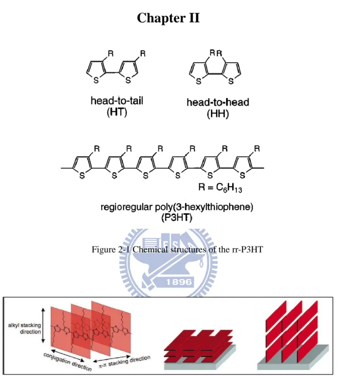
2-1 Chemical structure of SCLT materials
Most of organic devices is made by p-type material, therefore we chosen the most common soluble polymer, which is called regioregular poly(3-hexylthiophene). Soluble and processable poly~3-alkylthiophene!s have been found to have many potential applications such as light-emitting diodes, nonlinear optical devices, rechargeable battery electrodes, and field-effect transistors. The 3-alkyl substituents can be incorporated into a polymer chain with two different regioregularities: head to tail (HT) and head to head (HH). There are two kinds of P3HT that we can purchase, as in Fig.2-1, one is monomer HH compared to HT ratio about
7
1:1, which we called RD-P3HT(regionrandom-P3HT), another HT:HH is about 66:1, which we called RR-P3HT(regionregular-P3HT)[17]. When the HT side chain ratio is higher, mobility in FET becomes greater. Our P3HT is purchase from Sigma Aldrich Chemical Co. RR-P3HT, HT ratio is higher than 98.5%, meting point is 238℃, average molecular weight 87000, LUMO/HOMO equal 3.0/5.2.
Fluorene copolymers and polythiophenes have a relatively rigid backbone with attached alkyl chains for solubility, and are able to crystallize. Mobility is highly anisotropic as a result of chain packing in the crystallites. Charge transport is fastest in the conjugation direction as shown in Fig. 2-2 (a). When chains pack, the π-orbitals belonging to different polymer chains are stacked cofacially, and this partial overlap between π-orbitals assists interchain charge transfer. However, in another direction, the insulating alkyl chains impede charge transport so that mobility in this direction is the lowest. Such anisotropy has been experimentally verified by comparing the electrical characteristics of TFTs and diodes. Because of this pronounced anisotropy, texture and relative orientation of crystallites are expected to play an important role in controlling the electrical properties of these materials.[18]
In addition, in our experience for better performance, regioregular P3HT were purchased from Aldrich Chemical Co. and were used as received. When the storage environment oxygen and water concentration is too high, SCLT current may lower dramatically.
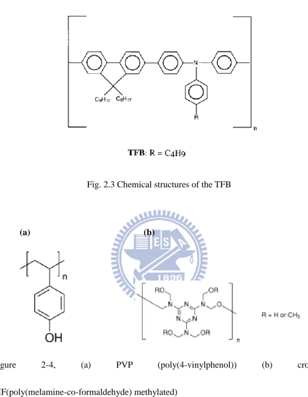
TFB (poly(9,9’-dioctylfluorene-co-N(4-butylphenyl)diphenylamine)) is another p-type material, which monomer is shown in Fig.2-3. The LUMO/HOMO is equal to 2.3/5.3 eV[19], which HOMO is higher than P3HT, and MoO3 work function is 5.4eV[20]. It’s suit for us to
8
PVP (poly(4-vinylphenol)) crosslink PMF(poly(melamine-co-formaldehyde) methylated) is our insulator layer. PVP melting point is 360℃, average molecular weight is 25000; PMF average molecular weight is 511. In our solution process, we mix PVP:PMF weight ratio11:4 and then spin on substrate, finally heat 200℃ one hour. It’s easy and stable after heating one hour. The PVP and PMF monomer is shown in Fig. 2-4.
2-2 Charge transport in polymeric semiconductor[21]
Conjugated polymers are intrinsically semiconducting materials. They lack intrinsic mobile charge, but are able to transport charge generated by light, injected by electrodes, or provided by chemical dopants. The main constituent of conjugated polymers is the carbon atom. It is the nature of the bonds between the carbon atoms that gives the conjugated polymer its interesting physical and chemical properties. To understand the basics of these molecular bonds it is instructive to understand the shape of the electronic orbitals of the atoms participating in the molecular bond.
Carbon, in the ground state, has four electrons in the outer electronic level. The orbitals of these electrons may mix, under creation of four chemical bonds, to form four equivalent degenerate orbitals referred to as sp3 hybrid orbitals in a tetrahedral orientation around the carbon atom, If only three chemical bonds are formed, they have three coplanar sp2 hybridized orbitals which are at an angle of 120o with each other. These bonds are called σ -bonds, and are associated with a highly localized electron density in the plane of the molecule. The one remaining free electron per carbon atom resides in the pz orbital,
perpendicular to the plane of the sp2 hybridization. The pz orbitals on neighboring atoms
overlap to form so-called π -bonds. A schematic representation of this hybridization is given for the simplest conjugated polymer, polyacetylene, in Fig.2-5.
9
Molecules with σ and π -bonds are schematically represented by single and double alternating chemical bonds between the carbon atoms, and are called conjugated molecules.
The π -bonds establish a delocalized electron density above and below the plane of the molecule. These delocalized π -electrons are largely responsible for the opto-electronic behavior of conjugated polymers.
2-3 Metal/polymer/metal schottky diode
There are two kinds of interface between organic and metal due to work function difference, one is ohmic contact, and the other is schottky contact. The simple result is shown in below graph.
We use p-type semiconductor as example (Fig.2-6, Fig 2-7). The Fermi-level of p-type semiconductor is lower than Fermi-level of metal. In the other way, work function of metal is smaller than work function of semiconductor (Φm < Φs). As a result, electron will diffused from metal to p-type semiconductor until balance. Now both Fermi-level equalized, the concentration of electrons at p-type semiconductor interface is higher. This interface depleted
10
in order to satisfy the continuous of vacuum energy (E0). So there is a barrier between metal and semiconductor. When we bias semiconductor a positive voltage, it would lower this energy barrier, and voltage large enough, holes in semiconductor will easily transport to metal electrode. In the other way, negative bias voltage will increase energy barrier, only little leakage current. We called Schottky contact here. And we discuss another case, the Fermi-level of p-type semiconductor is higher than Fermi-level of metal. In the other way, work function of metal is larger than work function of semiconductor ((Φm >Φs). Ideally, there are not energy barrier, so just like a resistance, current is proportional to voltage. As a result, we call this ohmic contact.
In our SCLT, this is an important mechanism for controlling leakage current.
2-4 Space charge limit current
The theory of space-charge-limited current between plane parallel electrodes was first given by Mott and Gurney (1940) and has been extended by several authors including Lampert (1956). In the absence of any trapping effects the current density is given by the Mott-Gurney Law
In the inorganic semiconductor materials, space charges may be received from cations and anions after the free charges counteraction in the interface of PN junction. But there is no PN junction in Organic semiconductor, so do not have the space charges which like depletion region. It was from the injection charge which cannot transport or recombine immediately, and accumulate in the metal-semi interface. As a result, it contains high carrier concentration in interface and charge back into the electrode, the formation of the loss. (Fig. 2-8)
SCLC easily occur in the following conditions, low-carrier injection barrier (<0.25eV). The interface between electrode and semiconductor is ohmic contact, the injection electrode
11
provides a large number of carrier and fill all the traps up, and the semiconductor material itself mobility is too low. Using the following modified Child's Law (Square-power Law) mathematical model of SCLC, trap-free and trap-trapped, respectively.
3 2 0
8
9
L
V
J
r
(1)Trap-free case: The assumption is that thermal free carriers and trapping states do not exist in
organic semiconductor materials.
Trapped case: (The assumption is that there are no thermal free carriers in organic
semiconductor materials. Under the conditions of shallow trap, the first deep trap has been filled.) 3 2 0
8
9
L
V
J
r
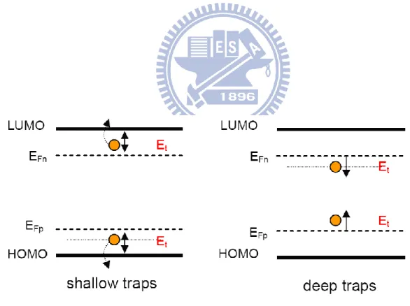
θ=free carriers / trapped carriers (2)Trap states in materials are from their own defects and impure materials. According to the relative position between e-holes of the trap states and the e-hole quasi-Fermi level can be divided into deep traps and shallow traps as in the Figure 2-9. J-V 2 shows a linear
12
relationship no matter traps exist or not. In fact, the mobility of semiconductor materials is a function contained temperature and electric field. As follow: (with holes for example).
In the above results, electrical devices are controlled by SCLC, the current density will enhance by high temperature and applied voltage.
13
Chapter II
Figure 2-1 Chemical structures of the rr-P3HT
Figure 2-2 (a) Crystallite structure in polythiophenes. The conjugation direction and the π-π
stacking direction are fast charge transport directions. Charge transport in the alkyl stacking direction is slower. (b) Plane-on and (c) edge-on texture of polymeric crystallites. In the plane-on texture, the alkyl stacking direction is in the plane of the substrate, which is bad for the current density in TFTs.
14
Fig. 2.3 Chemical structures of the TFB
(a) (b)
Figure 2-4, (a) PVP (poly(4-vinylphenol)) (b) crosslink
15
Figure 2.5 (a) The molecule are structure of polyacetylene, for clarity, hydrogen atoms are not shown. The alternating double and single bonds indicate that the polymer is conjugated. (b) Schematic representation of the electronic bonds in polyacetylene. The pz-orbitals overlap to
form π-bonds.
Fig. 2-6 band diagram of schottky contact
16
Figure 2-8 The injection charge which can not transport or recombine immediately, and accumulate in the metal-semi interface.
17
Chapter III
Devices Fabrication
We fabricated three different grid position devices(PVP 1000 Å ,1500 Å ,2000 Å ), and choose kinds of materials as emitter or collector. Because bottom electrode need to stand O2
plasma treatment, we don’t have plenty selection, now only aluminum and ITO is practical. Instead of bottom material, it’s free to choose top electrode. Basically we have to use high work function material as injection electrode because that our organic material is p-type. Gold is usually used, but gold has its own diffusion problem, so we add a MoO3 film. Furthermore,
MoO3 work function is higher than Au, it suits for else high HOMO materials. ITO with O2
plasma treatment need to spin P3HT layer immediately, or it will get worse injection. Compared to ITO, top injection MoO3 has an advantage that it has no quality time limit.
We named every layer and list all parameter in Fig.3-1 and Table 3-2. For varying grid position experiment, process is same as above, only change PVP thickness when spin coating. The PVP 2000Å conditions don’t need bottom SiOx strengthening layer, but 1000Å are still
needed. Bottom emitter electrode is ITO, top collector is Al. This top emitter SCLT (PVP, Al) is the most complicated device now, and else devices simplify layers or vary PVP thickness. Here we describe this devices process flow.
The process flow (Top emitter PVP1000, Al) is shown in Fig. 3-3. Poly (3-hexylthiophene) (P3HT) was used as polymer semiconductor material. The Al collector SCLT was fabricated on a glass substrate which has patterned Al by evaporation. 1000 Å cross-linkable poly(4-vinyl phenol) (PVP) was spin coated on the substrate, and then cross-linked at 200 degree C for 60
18
min in Glove Box environment. Poly (melamine-co-formaldehyde) methylated (Aldrich, Mw~511) is utilized as a crosslinking agent for PVP. The surface of PVP is turned into hydrophilic by short time exposure of 50 W O2 plasma before submerging the substrate into
2000 Å positively charged polystyrene spheres (Merck, K6-020) dilute ethanol solution with 0.8 wt %. The polystyrene spheres were adsorbed on PVP surface to serve as the shadow mask. After submerging the substrate for 3 minutes in polystyrene spheres solution, the substrate was then transferred into a beaker with boiling isopropanol solution for 10 s. The substrate was immediately blown dry to form two dimensional colloidal arrays. 100 Å SiOx first and 400 Å Al,
finally 400 Å SiOx were evaporated as lower insulator, metal base electrode and upper insulator
through the same mask. This strengthening 100Å SiOx layer is worth mentioning that 1000Å
PVP cannot afford dielectric property unless add 100 Å strengthening SiOx layer. After
removing the polystyrene spheres by an adhesive tape (Scotch, 3M), the PVP at sites without SiOx /Al/ SiOx coverage was removed by 13 min 150 W O2 plasma treatment. The substrate was
then stored in glove box for various time before spin coating P3HT of 3500 Å from 4.5 wt % chlorobenzene. Finally, the MoO3/Al emitter in same mask is deposited to complete the SCLT
with active area as 1 mm2.
Here we describe the easy case, bottom emitter SCLT(PVP2000). The SCLT was fabricated on an ITO glass substrate which is first flattened by 150 W O2 plasma for 30 min.
2000 Å cross-linkable poly(4-vinyl phenol) (PVP) is spin coated on the ITO substrate, and then cross-linked at 200 for 60 min in Glove Box environment. And following is same as above. “Insulator B” is unnecessary, and “Insulator A” increase from 400Å to 500Å . Noticeably, we need to spin P3HT immediately after O2 plasma etching. Because O2 plasma treatment on
ITO will increase the hole injection ability to P3HT by increase HOMO.[22] The real devices mask and porous structure is shown in Fig.3-5.
19
parameter.
3.1 ITO patterning
Our ITO substrate resistance is determined < 7 . We define and etching electrode and active area by shadow mask which is shown in Fig. First we divide ITO glass into 3×3 cm2 square, and then clean by soap, acetone, IPA solution in ultra sonic 10 to 20 minutes. Finally we use amount DI water to remove leftover solution, and dry by N2 air.
Put the clean ITO glass on 170℃ hotplate for 5 minutes at last, and stick negative PR when glass is hot. Next step is using UV lithography through defined shadow mask for 32 seconds. Immerse prepared 50mg K2CO3:1000ml water as develop solution for 50 to 80
seconds, and then clean by DI water. We need to remove residue PR and develop solution by tissue first, and then etching by HCl solution with 50℃ to 60℃ for 50 seconds. Finally remove PR by NaOH solution with 5wt%, and clean by DI water. We can get defined ITO pattern glass.
3.2 Material testing – MIM diode and mobility calculation
MIM diode is a simple way to test material characteristics, not only for insulator, but also organic compound. Through this diode, we can check mobility, polymer morphology, electrode injection ability, etc. Anyway, this diode is an important tool for researching SCLT, and we usually use this diode to determinate problem layer.
Figure 3-6shows the pattern of bottom electrode, top electrode, definition of active region. The pattern was defined by shadow mask and line width is 1 millimeter in active layer. In this step, ITO electrode is mentioned in section 3.1. The Al electrode is made by thermal evaporation. Top electrode is also made by thermal evaporation. The active region is define by cotton swabs if we are spinning polymer. In the other way, active mask is used when we
20
evaporated the material. The cross section is also shown in Fig.3-6.
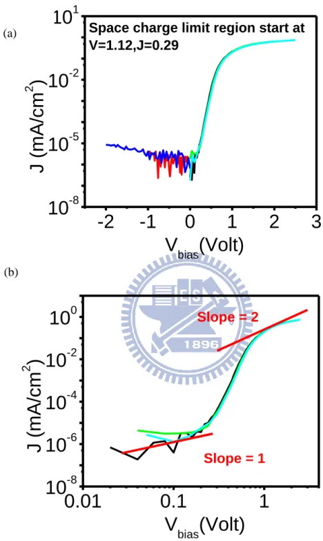
The most characteristic of diode is mobility, and we calculate mobility from diode by SCLC equation (Eq.1), which relative dielectric constant r is equal 3. This is the only way that we can calculate mobility, the common TOF method cannot work in this vertical devices. We measured diode byHP-5270. When we get data, we graph double log picture, find the point
equal to slope 2, which is turn into space charge limit current situation. Using Eq.1, we can get mobility. I show a diode example in Fig.3-7.
3.3 PVP treatment and insulating property
Cross-linkable poly(4-vinyl phenol) (PVP) is spin coated on the substrate, and then cross-linked at 200℃ for 60 min in Glove Box environment. Poly (melamine-co-formaldehyde) methylated (Aldrich, Mw~511) is utilized as a crosslinking agent for PVP.
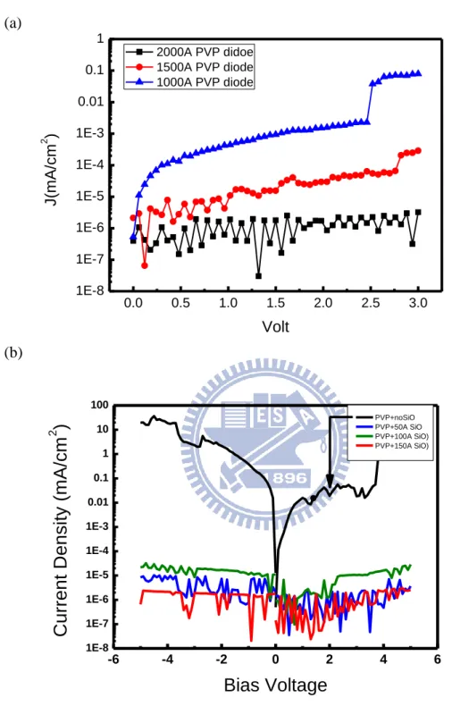
The diode with PVP as active area characteristic is shown in Fig3-8, and here we want to control leakage current under 10-4 mA/cm2 in SCLT. The PVP with thickness 2000Å is fine, but 1500Å , 1000Å are not acceptable. The SiOx is a very powerful insulator, so we add a thin
SiOx layer to thinner PVP insulator, finally we get a fine result. As in Fig.3-8, through this
diode I made has a rough ITO surface due to lack of O2 plasma treatment (so pure PVP 1000Å has a huge leakage current), it still convince us that thinner PVP plus 100Å SiOx is
promising and practical.
Next we need to coat PS ball on PVP surface, but PVP is hydrophobic, we need to transform PVP to hydrophilic. We have two selections, one is using UV-ozone and the other is O2 plasma. Both PS ball distributions are almost same, but UV-ozone will damage PVP
insulator, instead O2 plasma keeps well. As in Fig.3-9, we can see O2 plasma with 50 watts
21
3.4 Self-Assembling monolayer treatment
The self-assembled monolayer dielectrics chemical structure of n-octadecylphosphonic acid is shown in Fig. 3-9. We fabricate two kind of bottom diode electrode, and then immerse in 1mM n-octadecylphosphonic solution in acetone for 5 minutes. This SAMs reacts with oxide material. We can see this result, ITO reacts slowly but Al (or, Al2O3) react quickly. Due
to the breakdown curve, the SAMs coverage may be better on Al2O3. For our side well
22
Chapter III
Figure 3-1. The name of every layer, reflect to Table.
Name Metal A Material/ thickness(Å ) Metal B Metal C (grid) Layer A Insulator A Insulator B Insulator C Bottom emitter SCLT(PVP2000) Al / 400 ITO Al / 400 none SiOx / 500 none PVP / 2000 Bottom emitter SCLT(PVP1500) Al / 400 ITO Al / 400 none SiOx / 400 SiOx / 100 PVP / 1500 Bottom emitter SCLT(PVP1000) Al / 400 ITO Al / 400 none SiOx / 400 SiOx / 100 PVP / 1000 Top emitter SCLT(PVP2000,Au or Al) Al or Au /400 Al / 400 Al / 400 MoO3/ 400 SiOx / 500 none PVP / 2000 Top emitter SCLT(PVP1500,Au or Al) Al or Au /400 Al / 400 Al / 400 MoO3/ 400 SiOx / 400 SiOx / 100 PVP / 1500 Top emitter SCLT(PVP1000,Au or Al) Al or Au /400 Al / 400 Al / 400 MoO3/ 400 SiOx / 400 SiOx / 100 PVP / 1000
23
Figure 3-3 Process flow of top injection SCLT, notice that top emitter is a thin MoO3 layer
before Al electrode.
24
Figure 3-5 The (a) top view of SCLT (b) real PS ball distribution (c) cross section of SCLT (d)
the SEM of grid structure before P3HT spin coating.
Figure 3-6 The diode of (a) bottom electrode (b) top electrode (c) definition of active area (d)
25
-2
-1
0
1
2
3
10
-810
-510
-210
1J
(mA/
cm
2)
V
bias(Volt)
Space charge limit region start at
V=1.12,J=0.29
0.01
0.1
1
10
-810
-610
-410
-210
0Slope = 1
J
(mA/
cm
2)
V
bias(Volt)
Slope = 2
Fig. 3-7 A space charge limit diode (ITO/P3HT/Al) (a) log J-V curve (b)and double log J-V
curve, the slope=2 means the SCLC region (b)
26 0.0 0.5 1.0 1.5 2.0 2.5 3.0 1E-8 1E-7 1E-6 1E-5 1E-4 1E-3 0.01 0.1 1 J(mA/cm 2 ) Volt 2000A PVP didoe 1500A PVP diode 1000A PVP diode -6 -4 -2 0 2 4 6 1E-8 1E-7 1E-6 1E-5 1E-4 1E-3 0.01 0.1 1 10 100
C
u
rr
e
n
t D
e
n
s
ity (
m
A
/cm
2)
Bias Voltage
PVP+noSiO PVP+50A SiO PVP+100A SiO) PVP+150A SiO)Fig 3-8 Pure metal-insulator-metal diode result, (a) is PVP with 2000Å , 1500Å , 1000Å (b) is
PVP1000Å plus 0Å , 50Å , 100Å , 150Å SiOx.
(a)
27
-5 -4 -3 -2 -1 0 1 2 3 4 5
10
-810
-710
-6V(V)
J(
mA/
cm
2)
-5 -4 -3 -2 -1 0 1 2 3 4 5
10
-810
-710
-610
-510
-4V(V)
J(
mA/
cm
2)
Figure 3-9 Pure MIM(ITO/PVP/Al) diode, PVP with (a)O2 plasma 50W (b) UV-ozone treated
before Al electrode deposition (a)
28 -5 -4 -3 -2 -1 0 1 2 3 4 5
10
-510
-410
-310
-2J
(mA/
cm
2)
V -5 -4 -3 -2 -1 0 1 2 3 4 510
-610
-510
-410
-310
-210
10
-1 010
110
210
310
4J
(mA/
cm
2)
VFigure 3-10 (a) Chemical structure of n-octadecylphosphonic acid (b) SAMs treated MIM diode (Al/SAM/Al) insulating property (c) MIM (ITO/SAM/Al) insulating property.
(a)
(b)
29
Chapter IV
Result and discussion
4.1 Discussions that P3HT mobility varies with thickness
From this “thick” SCLT result, we see first current didn’t decrease as SCLC law predicting, from 1 to (L/L’)3. It means current will become 1/6 or 1/8, but result is not match. Of course, there are many variations and different between now and before devices; we still try diode structure, which is very simple. We are wondering if there is mobility improvement in thick P3HT, and therefore we fabricate different spin rate, solution weight percent, and the result is shown in graph 4-1(a) to 4-1(b). We doubt that the bulk P3HT has been different when will spin a thick P3HT film, so we take a UV-vis absorption spectrum (Fig.4-2), but the results can’t observe difference from thick and thin film. It’s also observed at thin film horizontal transistor, which is made by P3HT on silicon substrate .[23] But the conclusion of reference cannot explain this diode result. So it’s still a puzzle, but anyway, it benefits for our thick devices.
4.2 Grid position discussion
We think grid position is a very crucial parameter for SCLT, but we limit by the insulator thickness due to control leakage current, until we arrange a strengthen insulator layer above thinner PVP. Finally we can discuss this grid variation impact. Three grid position SCLTs were fabricated, we combined three results, and we graphed a picture like traditional Id-Vg here (Fig.4-3). The next step we calculate subthreshold swing (S.S.) and threshold voltage at “off-state” and “on-state”. The S.S. is easy to calculate, but the threshold voltage is difficult.
30
Because this SCLT is not suitable for MOSFET model here, we have to give a mathematical definition for our calculating.
,
at off state region
,
at on state regionWe list three bottom injection SCLTs results in Table 4-4.
We can see S.S is smaller at first when PVP is thicker. Thicker PVP means grid near to collector, in another way, the “tuning” channel length is longer, so the banding range is longer, too. Lower subtreshold swing is benefit for low power logic application, this parameter is important for our future work. The S.S. of CMOS is limit to 60mV/decade, and traditional a-Si:H TFT is around 500mV/decade, compare to OFET made by P3HT, also solution process, S.S is 1V/decade. Moreover, this device is fabricating on silicon wafer and using SiO2 thermal
dielectric, on/off ratio is 105. In addition, polymer dielectric devices, on/off ratio is smaller, S.S and driving voltage is higher. Here we can observe great potential for vertical transistor, every characteristic improve a lot.
Increasing PVP thickness benefits control ability, but decrease the output current density at on state region. Before we purposed a band diagram explanation, there is a question need to clarify. We are wondering P3HT coverage at this rough structure is not good because the solution surface tension, especially in higher PVP, made emitter contact area less. We have tried to take a SEM picture, but unfortunately, the cross section will be damage when we get sample because P3HT is polymer and flexible.
31
This question is solved until top injection SCLTs has been developed.
Actually the definition of is not good, because our devices has a limit that when we bias grid a negative voltage, the current will get into grid metal electrode. And the output current will effect by the grid leakage current. This ITO/P3HT/Al diode is very sensitive when the voltage difference is higher than 0.9 volts. If we bias more “on-state” voltage, the current gain will fall quickly, and devices may short, finally polymer will lost the semiconductor characteristic. This problem is difficult to solve, through I purposed a method in section 4.5, but it still cannot solve completely. If we can cover the side grid a powerful insulator in the future, maybe we can see more details at the on state region.
4.3 Electrode work function difference
Different work function electrodes devices are shown in Figure 4-5. We made two kinds of inverted SCLT, left is Al collector, right is ITO collector, and middle is changing collector and emitter probe when measuring. Plenty reference indicated MoO3 HOMO is 5.3 as hole transport
layer higher than ITO with O2 plasma treated 5.1. We can see if two electrodes work function
are similar, the on current curve rising very fast, also off current rising as well. In the other way, MoO3/Au electrode obviously control off current well. This result tell us that SCLT off state
mechanism: not only grid electric field, but built-in field plays an important role.
Interesting is, our devices actually inspired by vacuum tube, now it’s different between “traditional vacuum tube” from “semiconductor vacuum tube” here. By this inversed structure, we finally can discuss the impact of electrode. As mentioned before, we don’t have plenty choice for bottom electrode. Moreover, upside electrode cannot use gold like materials because diffusion. Here we purposed an efficient method to change electrode material. Though performance are not still good compared to before structure, it’s potential for more application in the future due to higher HOMO especially synthesizing polymer material technology
32
developing so quickly. In addition, if we use inverted structure, we can avoid the quality time of ITO with plasma treatment, which are needed to spin immediately after O2 plasma etching.
The reason of on/off ratio decreasing is the O2 plasma etching. Because Al emitter will suffer
an O2 plasma over etching when we removed PVP. It’s a simple test; we made a diode of
Al/P3HT/MoO3/Al, the bottom with O2 plasma and without O2 plasma. The diode with O2
plasma treatment current decrease and has an obvious trapping.
And we made two grid position top emitter SCLTs. The higher grid (means grid near to emitter) has higher current output instead of lower grid in bottom injection SCLTs results. Now we believe that the grid position dominating the current output characteristic.
From our experiment results, unfortunately on/off ratio seems related to PS ball distribution well
As we show in Table 4-4, now the on/off ratio is about 105. The PVP 2000 Å SCLT’s samples are amount, so the best result is not surprised. We do not sure the limit because the PS distribution is random. The lower on/off ratio devices is usually due to control ability losing, which means off state completely out of control but instead off grid leakage current.
Combine top and bottom injection SCLTs result, we purposed a explanation in next section.
4.4 Band diagram in SCLT
We purposed a band diagram in Fig.4-6
In off state situation, the barrier is longer when grid near collector. As a result, off state control better in PVP 2000Å case. If grid is arranged at high position (near collector, Al), the hole carrier will transport more difficulty. In addition, we discover in Fig.3, higher grid let devices’ S.S. became small, it convince us higher position(near collector) control current more efficiently. But higher position is a disadvantage for on state situation, as shown in above
33
diagram, grid position are needed to bias more “negative” voltage in order to completely “open” whole channel. The limit of bias is that ITO(emitter, ground)/P3HT/Al(grid, bias) is not completely insulated. We cannot bias too negative voltage, or it would be dominated by this emitter-grid diode. This phenomenon limits this devices operating range which cannot reach saturation region. If we can solve this insulator problem, the control ability of device will improve (now on/off ratio can reach around 1x10⁵), and this devices would have more application.
4.5 SAMs treatment
For increasing current gain, we try to cover grid completely. As in chapter mentioned, SAMs is sensitive to Al than ITO, we use this SAMs to cover grid structure a monolayer insulator.
This treatment is for dichlorobenzene (DCB) solvent annealing device. The same structure of bottom injection PVP2000 SCLT, but DCB solution using, which dried slowly, made P3HT better ordering and crystallinity in their solid states. In our results, compare to chlorobenzene solution SCLTs, the grid leakage current is large. Therefore we’d like to use SAMs to enhance current gain, especially when devices operating at on-state. The result is shown in figure 4-8. As a result, SCLT grid leakage current at on state decrease about one order, furthermore, this structure is furthermore extremely simple. Without upper insulator, it only uses n-octadecylphosphonic acid solution to “deposit” insulator layer. We added SiOx
100Å layer beneath Al grid in order to avoid the leakage current from emitter to grid by PVP. It helped us identify that SAMs work or not. And we observed that leakage current is higher than 10-4 mA/cm2, as a result, the SiOx 100Å would not be necessary anymore. So we build a
simple SCLT process that is with acceptable on/off ratio(>3×10⁴)(Fig 4-8, and without SAMs treatment, using PVP2000 bottom injection structure is Fig 4-9), current gain(>3×10⁵), and
34
large output current(>15 mA/cm2). But there is incompatible here, ITO with O2 plasma
treatment cannot stand for long time, the hole injection enhancement decreasing with time. And our SAMs immerse 5 min obviously give a injection barrier for ITO to P3HT, so the characteristic of SCLT get worse here. If we cannot change ITO electrode material, and this problem would be tough for good. Maybe top injection SCLT is a solution for this problem.
Finally, this SAMs treatment SCLT is more simple and have a high potential that completely solution process. In our future work, that is using special “lithography” method to replace PS balls coating, which is extremely useful.
35
Chapter IV
500 1000 1500 2000 2500 3000 3500 4000 1E-5 1E-4 2.5% wt 3.5% wt 4.5% wt P3 H T mo b ili ty (cm 2 /V-s) P3ht thickness (A) 20000 30000 40000 50000 60000 70000 80000 90000 100000 110000 1E-5 1E-4 2.5% wt 3.5% wt 4.5% wt Mobility (cm 2 /V-s)E-field (Volt/cm)
(a) (b)36 0 2000 4000 0 1 2 P3HT 2.5wt % P3HT 3.5wt % P3HT 4.5wt %
Second order voltage (volts)
P3ht thickness (A)
Fig 4-1 Diode structure which is (a) different mobility vary with thickness. Here we can see mobility increase with thickness (b) Different mobility vary with electrical field. (c) the voltage of second order value vary with thickness.
400 600 800 1000 1200 0.0 0.2 0.4 0.6 0.8 1.0 CB P3HT 1500A Normalized Wavelength (nm) CB P3HT 3500A
Fig 4-2 UV-vis absorption spectrum of different thickness P3HT on ITO (c)
37 -1 0 1 2 3 4 5 1E-5 1E-4 1E-3 0.01 0.1 1 10 100 O u tp u t cu rre n t d e n si ty (mA/ cm 2 ) Bias voltage(volts) PVP2000,Vc=2.4V PVP1500+SiOx,Vc=2.66V PVP1100+SiOx,Vc=2.66V
Fig 4-3 Output current of different SCLT vary with grid voltage at similar voltage
Name(bottom
injeciton)
S.Swing VT-on state
(volt) VT-off state (volt) on/off ratio PVP1000 340mV -0.62 1.86 84000 @ 2.4V PVP1500 301mV -0.60 1.45 100000 @ 3.36v PVP2000 174mV -0.70 0.42 200000@ 1.9V Table 4-4 Different SCLT calculating results
38 0 1 2 3 4 1E-6 1E-5 1E-4 1E-3 0.01 0.1 1 10
Step= 0.50V
Vb= 2.8V
Vb= -0.2V
Vb= 2.1V
Collector current density (mA/cm
2 )
-Vc (Volts)
Vb= -1.2V
Step= 0.55V
0 1 2 3 4-Vc (volts)
3 2 1 0 -1 -2 1E-6 1E-5 1E-4 1E-3 0.01 0.1 1 10Vc = 0V
Collector current density (mA/cm
2 )
Grid voltage (volts)
Vc = 3.6V
Step= -1.2V
4 3 2 1 0 -1
Grid voltage(volts)
Fig 4-5 Left is Al as collector, right is ITO as collector. (a) output current varies with voltage from emitter to collector, and step by grid voltage. (b) is like Id-Vg, output current varies with grid voltage, and steps by voltage from emitter to collector.
(a)
39
Fig 4-6 A band diagram for (a)grid near to collector and (b) grid near to emitter. Upside means off state band, beneath off-state is on state. For on state, in order to get the same slope banding, the grid voltage must bias more “negative”.
40 0 1 2 3 4 5 1E-7 1E-6 1E-5 1E-4 1E-3 0.01 J b at on state -0.90V -0.05V 0.80V 1.65V 2.50V 3.35V 4.20V |J b | (mA/cm 2 ) Vc J b at on state 0 1 2 3 4 5 1E-7 1E-6 1E-5 1E-4 1E-3 0.01 -0.90V -0.05V 0.80V 1.65V 2.50V 3.35V 4.20V |J b | (mA/cm 2 ) Vc
J
bat on state
Fig 4-7 The grid leakage current (a) SAMs treatment and (b) without treatment (a)
41
0
1
2
3
4
5
10
-610
-410
-210
010
2 -1.70V -0.60V 0.50V 1.60V 2.70V 3.80V 4.90V A bs( J c )-Vc
-2 -1 0
1
2
3
4
5
10
-510
-410
-310
-210
-110
010
1V
B(Volt)
J
c(mA/
cm
2)
0V 1.7V 3.3V 5.0V VC step 1.66 voltFig 4-8 SCLT with SAMs treatment, (a) is output current vary with voltage from emitter to collector, and step by grid voltage. Notice that our grid voltage add to -1.7V (b) is like Id-Vg, output current varies with grid voltage, and step by voltage from emitter to collector.
(b) (a)
42
0
1
2
3
4
5
10
-610
-410
-210
010
2 -0.90V -0.05V 0.80V 1.65V 2.50V 3.35V 4.20V A bs( J c )-Vc
V
Bstep 0.85 volt
Fig 4-8 SCLT without SAMs treatment, output current varies with voltage from emitter to collector, and step by grid voltage.
43
Chapter V
Conclusion
We have fabricated a high on/off ratio SCLT from 2×10⁴ to 2×10⁵. More important is the yield, we demonstrated a reliable and easy process. To achieve this result, we modified and optimized every parameter in SCLT. Compared to P3HT horizontal TFT, our performance is tremendously well. From the starting chapter, we pursued a high on/off ratio, high output current, and low cost devices, thus we cannot achieve all best results at same time, but we still reached every goal from the following experiment.
By this mature process, we varied grid positions, and we knew that grid position adjust on and off state voltage, impact subtreshold swing voltage. This is important for future device designing, especially analog devices. Second is purposed an inverted (top injection SCLT) structure here. Before this device, many methods have been tried. This top injection SCLT is useful for new polymer as active layer, especially air stable polymer.Although we noticed that current would be lower if Al electrode had been treated by O2 plasma. Third is an extremely
simple devices, we used n-octadecylphosphonic replacing SiOx layer. This devices is very
suitable for large area fabrication, although performance is not good, but acceptable. The only one vacuum deposition process is the Al grid and Al emitter layer, and the Al deposition requirement is cheap. The goal of “all solution process” is possible if we can find a method to replace this Al deposition.
In the future, we will try smaller porous structure. We can get dramatically improve when decreasing the radius of PS ball (the “hole” of channel) base on a very tentative simulation (Appendix). Maybe SAM treatment is suit for this small radius structure, because
44
the small PS ball limits the grid and insulator thickness to PS ball’s radius.
Another way is using soft lithography to define the porous. As we mentioned, PS ball distribution is random, we’d like to control this distribution from random to ordering.
45
Chapter VI
Appendix
Figure A-1 Various structures simulation results
This is very a very tentative simulation. A lot of conditions SCLTs have been simulated, through not completely match our result, but acceptable. The blue one is our bottom injection SCLT, and the lowest one is scale down this PVP2000 bottom injection SCLT to PVP1000, and the hole radius decrease from 100nm to 50nm, P3HT thickness also decrease. We can see on/off ratio is dramatically increasing. Practically this smaller devices is hard to control the insulator breakdown, hope this problem can be solved in the future.
Appreciate Lin’s simulation.
Raius 50nm PS ball
47
[1] T. Miyadera, T. Minari, K. Tsukagoshi, H. Ito, and Y. Aoyagi, "Frequency response analysis of pentacene thin-film transistors with low impedance contact by interface molecular doping," Applied Physics Letters, vol. 91, p. 013512, 2007.
[2] J. Lee, J. Kim, S. Im, and D. Jung, "Threshold voltage change due to organic-inorganic interface in pentacene thin-film transistors," Journal of Applied Physics, vol. 96, p. 2301, 2004.
[3] G. Gu and M. Kane, "Moisture induced electron traps and hysteresis in pentacene-based organic thin-film transistors," Applied Physics Letters, vol. 92, p. 053305, 2008.
[4] D. Hwang, K. Lee, J. Kim, S. Im, C. Kim, H. Baik, J. Park, and E. Kim, "Low-voltage high-mobility pentacene thin-film transistors with polymer/high-k oxide double gate dielectrics," Applied Physics Letters, vol. 88, p. 243513, 2006.
[5] J. Collet, O. Tharaud, A. Chapoton, and D. Vuillaume, "Low-voltage, 30 nm channel length, organic transistors with a self-assembled monolayer as gate insulating films," Applied Physics Letters, vol. 76, p. 1941, 2000.
[6] M. Austin and S. Chou, "Fabrication of 70 nm channel length polymer organic thin-film transistors using nanoimprint lithography," Applied Physics Letters, vol. 81, p. 4431, 2002.
[7] H. W. Zan, K. H. Yen, P. K. Liu, K. H. Ku, C. H. Chen, and J. Hwang, "Low-voltage organic thin film transistors with hydrophobic aluminum nitride film as gate insulator," Organic Electronics, vol. 8, pp. 450-454, 2007.
[8] H. Ma, O. Acton, G. Ting, J. Ka, H. Yip, N. Tucker, R. Schofield, and K. Alex, "Low-voltage organic thin-film transistors with π-σ-phosphonic acid molecular dielectric monolayers," Applied Physics Letters, vol. 92, p. 113303, 2008.
48
[9] M. D. Austin and S. Y. Chou, "Fabrication of 70 nm channel length polymer organic thin-film transistors using nanoimprint lithography," Applied Physics Letters, vol. 81, p. 4431, 2002.
[10] L. Ma and Y. Yang, "Unique architecture and concept for high-performance organic transistors," Applied Physics Letters, vol. 85, p. 5084, 2004.
[11] Y. Chao, M. Xie, M. Dai, H. Meng, S. Horng, and C. Hsu, "Polymer hot-carrier transistor with low bandgap emitter," Applied Physics Letters, vol. 92, p. 093310, 2008.
[12] S. Cheng, Y. Chuang, K. Dhananjay, C. Ou, M. Wu, and C. Chu, "Organic Base Modulation Triodes and Their Inverters on Flexible Substrates," Advanced Materials, vol. 21, pp. 1860-1864, 2009.
[13] K. Fujimoto, T. Hiroi, K. Kudo, and M. Nakamura, "High-performance, vertical-type organic transistors with built-in nanotriode arrays," Advanced Materials, vol. 19, pp. 525-530, 2007.
[14] Y. Chao, H. Meng, and S. Horng, "Polymer space-charge-limited transistor," Applied Physics Letters, vol. 88, p. 223510, 2006.
[15] K. Ng, "Complete guide to semiconductor devices, 2002," New York.
[16] W. Shockley, "Transistor electronics: imperfections, unipolar and analog transistors," Proceedings of the IRE, vol. 40, pp. 1289-1313, 1952.
[17] Z. Bao, A. Dodabalapur, and A. Lovinger, "Soluble and processable regioregular poly (3 hexylthiophene) for thin film field effect transistor applications with high mobility," Applied Physics Letters, vol. 69, p. 4108, 1996.
[18] A. Salleo, "Charge transport in polymeric transistors," Materials Today, vol. 10, pp. 38-45, 2007.
49
transport fluorene-triarylamine copolymers," Advanced Materials, vol. 11, pp. 241-246, 1999.
[20] S. Tokito, K. Noda, and Y. Taga, "Metal oxides as a hole-injecting layer for an organic electroluminescent device," JOURNAL OF PHYSICS-LONDON-D APPLIED PHYSICS, vol. 29, pp. 2750-2753, 1996.
[21] C. Tanase, P. Blom, E. Meijer, and D. de Leeuw, "Charge transport in disordered organic field-effect transistors," Order, vol. 501, p. 2589.
[22] H. Yu, X. Feng, D. Grozea, Z. Lu, R. Sodhi, A. Hor, and H. Aziz, "Surface electronic structure of plasma-treated indium tin oxides," Applied Physics Letters, vol. 78, p. 2595, 2001.
[23] H. Jia, S. Gowrisanker, G. Pant, R. Wallace, and B. Gnade, "Effect of poly (3-hexylthiophene) film thickness on organic thin film transistor properties," Journal of Vacuum Science & Technology A: Vacuum, Surfaces, and Films, vol. 24, p. 1228, 2006.
![Figure 1. Schematic device structures. (a) Vertical transistor with rough source metal [10]](https://thumb-ap.123doks.com/thumbv2/9libinfo/8762370.208482/16.892.139.805.330.707/figure-schematic-device-structures-vertical-transistor-rough-source.webp)