754 IEEE MICROWAVE AND WIRELESS COMPONENTS LETTERS, VOL. 15, NO. 11, NOVEMBER 2005
A Dual-Mode Truly Modular Programmable
Fractional Divider Based on a
1/1.5 Divider Cell
Yu-Che Yang, Shih-An Yu, Tao Wang, and Shey-Shi Lu
Abstract—A divide-by-1/1.5 divider cell using a dual
edge-trigger technique is proposed. Based on this divider cell, a dual-mode programmable divide-by- circuit is demonstrated in 0.18- m CMOS technology, where = or .5 in one mode and 2 or 2 +1 in the other mode with = 128–255. When operated in the divide-by-2 2 +1 mode, this circuit outputs a signal with 50% duty cycle. Theoretically, can be any arbitrary and programmable integer.
Index Terms—50% duty cycle and phase-locked loop (PLL),
fractional divider, programmable divider.
I. INTRODUCTION
C
ONVENTIONAL fractional- phase-locked loops (PLLs) are mainly based on a fractional divider com-posed of an integer- divider and a – modulator [1], [2], where the former is modulated by the latter so that the desired fractional division ratio is obtained. However, since the intrinsic division ratio of the divider is still an integer, the quantization noise is inevitably introduced, and hence, contributes to the total phase noise of the PLL. To suppress the quantization noise, a fractional divider with intrinsically fractional division ratios, which we call intrinsic fractional divider for the ease of later discussions, is needed.In this work, a novel 1/1.5 divider cell is proposed. Based on this divider cell, an intrinsic fractional divider with a di-viding range of 128–255.5 and a step size of 0.5 was realized in 0.18- m CMOS technology. It is predicted that the quantiza-tion noise in a fracquantiza-tional- PLL using this intrinsic fractional divider in conjunction with a – modulator is 6 dB smaller than that in a conventional fraction- PLL due to the intrinsic fractional modulus.
There is also a need of integer- dividers with 50% duty-cycle [3]. In fact, a divide-by-three circuit with 50% duty duty-cycle has been published [3]. However, to our knowledge, a 50% duty cycle divide-by-odd number circuit with the odd number other than three has not been reported. Another important applica-tion of the proposed 1/1.5 divider cell is in generating 50% duty-cycle output signals from a divide-by- circuit, where is an arbitrary integer. In this letter, a 50% duty cycle pro-grammable divide-by- circuit 256–511 as well as a Manuscript received April 19, 2005; revised August 8, 2005. This work was supported by Grant 93-S-B62. The review of this letter was arranged by Asso-ciate Editor F. Ellinger.
The authors are with the Graduate Institute of Electronics Engineering, De-partment of Electrical Engineering, National Taiwan University, Taipei, Taiwan, R.O.C. (e-mail: [email protected]).
Digital Object Identifier 10.1109/LMWC.2005.858978
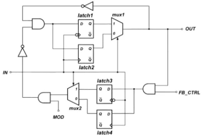
Fig. 1. Schematic of 1/1.5 divider cell.
50% duty cycle divide-by-three circuit based on the 1/1.5 di-vider cell is demonstrated. Theoretically, can be any arbitrary and programmable integer.
II. CIRCUITDESIGN
A. 1/1.5 Divider Cell
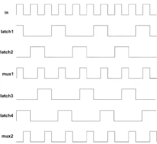
The key operating principle of the 1/1.5 divider cell is to trigger the divider either on the rising or falling edge of the input signal. Fig. 1 shows the schematic of the 1/1.5 divider cell, which consists of two multiplexers (mux), four latches, and threeANDgates. This structure is similar to the 2/3 divider cell in [4], but the serially-connected latches in [4] are replaced by par-allel-connected latches in combination with a multiplexer. One of the latches is enabled by the positive edge, and the other is enabled by the negative edge of the input signal with their out-puts selected by the multiplexer. When MOD and FB CTRL are both high, the divider is in the divde-by-1.5 mode with its timing chart illustrated in Fig. 2, where the operation of divide-by-1.5 can be clearly traced. When either MOD or FB CTRL is low, the output signal of latch1 remains high (or low) while the latch2 stays low (or high) and the feedback signal from the bottom of Fig. 1 is always high. Thus, theOUTsimply tracks the input signal, i.e., divided by 1. The source-coupled-logic (SCL) con-figuration [4] is adopted for the latch used in the 1/1.5 divider because of its high-frequency characteristic resulted from the constant supply current and differential voltage swing opera-tion.
B. Dual-Mode Programmable Fractional Divider
Based on the 1/1.5 divider cell, a dual-mode truly modular programmable fractional divider can be implemented. The first 1531-1309/$20.00 © 2005 IEEE
YANG et al.: DUAL-MODE TRULY MODULAR PROGRAMMABLE FRACTIONAL DIVIDER 755
Fig. 2. Timing chart of the 1/1.5 divider cell in divide-by-1.5 mode.
Fig. 3. Core of the proposed divider (divider core).
mode of this divider is to achieve intrinsic fractional modulus and the other is to generate 50% duty-cycle output signals in all integer modulus. The core of the programmable divider (Divider Core) is depicted in Fig. 3. The operation of this architecture is similar to the one described in [4] except that an additional 1/1.5 divider cell is placed in front of a chain consisting of 2/3 divider cells. The period of the output signal can be shown to be
MOD
MOD MOD MOD (1)
where is the period of the input signal and MOD , and MOD are the modulus control signals for the divider cells. From (1), it can be seen that the division ratio ranges from 2 to 2 1 0.5 with a step size of 0.5 (a fractional number). For a – modulator fractional divider, the output frequency is
(2) where is the divider output frequency, is the input fre-quency, is a fixed ration, and is the bit stream generated from the – modulator, which is a modulated form of a frac-tional number . The average output frequency is
(3) Assuming , the frequency error caused by dithering (4) (5) (6)
Fig. 4. Complete schematic of the programmable divider.
where . Consider how the frequency dithering is transformed to phase noise
(7) (8) (9) (10) where represents the power spectral density (PSD) of and denotes Fourier transform. According to the differen-tiate rule of Fourier transform
(11) Based on (6), can be written as
(12) Combine the previous two equations
(13) We can relate the with the DSM output bit stream
(14) Clearly, the phase noise contributed by the fractional divider can be lowered by 6 dB if with a step size of 1 is replaced by with a step size of 0.5. The complete schematic of the dual mode programmable divider is shown in Fig. 4. A strobe circuit, consisting of two parallel latches and a mux, is connected at the output of the divider core in order to resynchronize the output signal of the divider core by the input signal, and thus lowering the jitter accumulated in the divider core. A SCL-to-CMOS circuit translates the source coupled logic to standard CMOS logic signals (fractionalOUT) and functions as an output buffer. The other mode of the proposed programmable divider is to di-vide the input signal by an integer with a 50% duty-cycle even when the division ratio is an odd integer. This is achieved by dividing the FractionalOUTsignals by two as shown in Fig. 4. With this additional divide-by-two circuit, the output period are now two times of , and hence the division ratio becomes 2 1–2 2 1 but with 50% duty cycle output signals even with an odd division ratio.
III. MEASUREDRESULTS
To verify the function of the 1/1.5 divider cell, the dual mode programmable fractional divider as well as the 50% duty cycle divide-by-three circuit is implemented in a standard 0.18- m
756 IEEE MICROWAVE AND WIRELESS COMPONENTS LETTERS, VOL. 15, NO. 11, NOVEMBER 2005
Fig. 5. Die photo of dual mode programmable fractional divider.
Fig. 6. Measured 50% duty cycle output waveform (871 MHz) of divide-by-three circuit when a 2.6-GHz input signal is applied. Note that 50% duty cycle is achieved.
Fig. 7. Measured output waveform (10.02 MHz) of the programmable divider with modulus= 255.5 when a 2.56-GHz input signal is applied.
CMOS process. Fig. 5 shows the die photo of the dual mode programmable fractional divider. The divide-by-three circuit is operated at 1.8 V while the dual mode programmable fractional divider at 2.2 V.
When an input signal with a 2.6-GHz frequency is applied to the divide-by-three circuit, the measured output waveform is shown in Fig. 6, where a signal with one-third frequency (871 MHz) of the input signal (2.6 GHz) is observed. It is also clear that the 50% duty cycle is obtained at the same time. The programmable divider was implemented with 8 b, including one 1/1.5 divider cell and seven 2/3 divider cells. According to (1), the division range is from 128 to 255.5 in the fractional division mode and from 256 to 511 in the integer division mode. Fig. 7 shows output waveform of the programmable divider when the modulus of the divider is set to be 255.5 and an input signal with a 2.56-GHz frequency is applied. From Fig. 7, it can be seen the output frequency is 10.02 MHz, corresponding to the right divi-sion ratio. Fig. 8 shows output waveform of the programmable divider when the modulus of the divider is set to be 511 and an input signal with a 1.28-GHz frequency is applied. The output frequency is 2.504 MHz, corresponding to 1/511 of the input
Fig. 8. Measured output waveform (2.504 MHz) of the programmable divider with modulus= 511 when a 1.28-GHz input signal is applied.
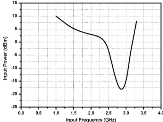
Fig. 9. Measured input sensitivity of the programmable divider.
frequency. Note that 50% duty cycle is achieved. The input sen-sitivity curve of the programmable divider is shown in Fig. 9. The measured operating range is from 1 to 3.3 GHz.
IV. CONCLUSION
A proto-type dual mode programmable fractional divider based on 1/1.5 divider cell is demonstrated in 0.18- m CMOS technology. In the fractional division mode, input signals up to 3.3 GHz can be divided by 128–255.5 with a step size of 0.5. Phase noise contributed by this intrinsic fractional divider in conjunction with a – modulator in a PLL is expected be lowered by 6 dB compared to the conventional integer divider in conjunction with a – modulator. In the integer division mode, 50% duty cycle output signals can be obtained after dividing the input signal by 256–511 with a step size of 1. A divide-by-three circuit with 50% duty cycle output signals based on 1/1.5 divider cell is also reported.
REFERENCES
[1] A. D. Riley, A. Copeland, and A. Kwasniewski, “Delta-sigma modula-tion in fracmodula-tional-n frequency synthesis,” IEEE J. Solid-State Circuits, vol. 28, no. 5, pp. 553–559, May 1993.
[2] P. Kenny, A. D. Riley, M. Filiol, and A. Copeland, “Design and realiza-tion of a digital1-6 modulator for fractional-n frequency synthesis,” IEEE Trans. Veh. Technol., vol. 48, no. 2, pp. 510–521, Mar. 1999. [3] R. Magoon and A. Molnar, “RF local oscillator path for GSM direct
con-version transceiver with true 50% duty cycle divide by three and active third harmonic cancellation,” in Proc. IEEE RFIC Symp., Jun. 2002, pp. 20–23.
[4] S. Vaucher, I. Ferencic, M. Locher, S. Sedvallson, U. Voegeli, and Z. Wang, “A family of low-power truly modular programmable dividers in standard 0.35-um CMOS technology,” IEEE J. Solid-State Circuits, vol. 35, no. 7, pp. 1039–1045, Jul. 2000.