Quasiregular quantum-dot-like structure formation with postgrowth thermal
annealing of InGaN
Õ
GaN quantum wells
Yen-Sheng Lin, Kung-Jen Ma, and Cheng Hsu
Department of Mechanical Engineering, Chung Cheng Institute of Technology, National Defense University, Tahsi, Taoyuan, Taiwan, Republic of China
Yi-Yin Chung, Chih-Wen Liu, Shih-Wei Feng, Yung-Chen Cheng, C. C. Yang,a) and Ming-Hua Mao
Department of Electrical Engineering, Graduate Institute of Electro-Optical Engineering, and Graduate Institute of Electronics Engineering, National Taiwan University, I, Roosevelt Road, Section 4,
Taipei, Taiwan, Republic of China
Hui-Wen Chuang, Cheng-Ta Kuo, and Jian-Shihn Tsang
Advanced Epitaxy Technology Inc., Hsinchu Industrial Park, Taiwan, Republic of China Thomas E. Weirich
The Center of Electron Microscopy, Aachen University of Technology, Ahornstrasse 55, D-52074 Aachen, Germany
共Received 22 October 2001; accepted for publication 5 February 2002兲
Postgrowth thermal annealing of an InGaN/GaN quantum-well sample with a medium level of nominal indium content共19%兲 was conducted. From the analyses of high-resolution transmission electron microscopy and energy filter transmission electron microscopy, it was found that thermal annealing at 900 °C led to a quasiregular quantum-dot-like structure. However, such a structure was destroyed when the annealing temperature was raised to 950 °C. Temperature-dependent photoluminescence共PL兲 measurements showed quite consistent results. Blueshift of the PL peak position and narrowing of the PL spectral width after thermal annealing were observed. © 2002 American Institute of Physics. 关DOI: 10.1063/1.1467983兴
Quantum-dot-like structures have been observed in InGaN/GaN quantum wells 共QWs兲. Such structures are formed because of the large lattice mismatch between InN and GaN.1–3 With high-resolution transmission electron mi-croscopy共HRTEM兲, randomly distributed clusters of indium aggregation and phase-separated InN were widely observed. The cluster structures form potential minimums共called local-ized states兲 for trapping carriers for efficient photon emission.4 –7 Such indium-aggregated distributions are basi-cally located in the quantum-well layers; however, they usu-ally diffuse into barriers, extensively under certain condi-tions. Typically, such out-diffusion becomes more extensive in a sample with a higher nominal indium content.3
It has been reported that postgrowth thermal annealing could alter the sizes and distributions of self-organized InAs quantum dots.8,9 In InGaN compounds, postgrowth thermal annealing processes for changing cluster structures and their photon emission properties were also reported.10–12In one of the previous results, a better-confined quantum-well struc-ture, i.e., weaker indium out-diffusion, after thermal anneal-ing was reported.12 The photoluminescence 共PL兲 intensity was increased with the stronger quantum-well confinement effect. Postgrowth thermal annealing can provide means for device manufacturers to tune the photon emission wave-length or to tailor the gain spectrum by changing the size/ composition of the quantum-dot-like structures. The infor-mation of thermal annealing is also helpful for crystal
growers to design growth procedures. In this letter, we report the formation of quasiregular quantum-dot-like structures from randomly distributed indium-aggregated clusters after postgrowth thermal annealing of an InGaN/GaN QW sample. It was found that with thermal annealing temperature at 900 °C, indium distribution was better confined in the quantum-well layers. Although the better confinement in a high-indium sample 共⬎45%兲 has been reported,12the obser-vation of quasiregular quantum-dot-like structures has never been reported. In particular, the indium content of our sample is much lower 共19%兲. Also, we found that such a trend of regular structure disappeared when the thermal annealing temperature was 950 °C. The measurements of optical prop-erties showed quite a consistent trend.
The sample used in this study was grown with a low-pressure metal–organic chemical-vapor deposition reactor. The InGaN/GaN QW sample consisted of ten periods of In-GaN wells with 3.5 nm thickness. The barrier was 10 nm GaN. In the sample, the QW layers were sandwiched be-tween a 1.5m GaN buffer layer on a共0001兲 sapphire sub-strate and a 50 nm GaN cap layer. The growth temperatures were 1010 and 720 °C for GaN and InGaN, respectively. The designated indium content of the sample was about 19%. As-grown samples were thermally annealed in a quartz tube furnace at different temperatures ranging from 800 to 950 °C in nitrogen ambient for 30 min. HRTEM and energy filter transmission electron microscopy 共EFTEM兲 were used to characterize material structures.
For HRTEM observation, cross-sectional samples were prepared in the conventional manner by grinding, dimpling,
a兲Electronic mail: ccy@cc.ee.ntu.edu.tw
APPLIED PHYSICS LETTERS VOLUME 80, NUMBER 14 8 APRIL 2002
2571
and Ar⫹-ion milling with 6 kV, 1 mA, and an incident angle of 4°. Based on previous experiences, for samples containing indium, the ion-milling step needs to be carried out with the specimen holder at liquid-nitrogen temperature in order to minimize ion-beam damage. The HRTEM investigations were conducted with a 200 keV Philips CM 200 and a 300 keV JEM 3010 microscope. All the high-resolution micro-graphs were taken at Scherzer defocus and the sample was viewed along a 关11–20兴 zone axis. The 300 keV JEM 3010 microscope was equipped with a 2 k⫻2 k slow-scan charge-coupled-device camera and a Gatan imaging filter共GIF兲. Re-garding the EFTEM images, the drift between the two preedge and the postedge images was recorded by using the cross-correlation algorithm available in the Digital Micro-graph software of the GIF. In order to remove the back-ground contribution underneath the ionization edges and to obtain elemental maps, the jump-ratio method was used to avoid noise and artifacts. However, it cannot be quantified.
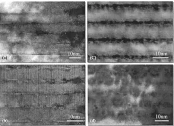
Figures 1共a兲–1共d兲 show the HRTEM bright-field images of the as-grown 共a兲, 800 °C-annealed 共b兲, 900 °C-annealed
共c兲, and 950 °C-annealed 共d兲 samples. The contrast variations
in the pictures represent the fluctuations of indium composi-tion. The diffusive InGaN/GaN QW interfaces can be clearly seen in the as-grown sample关Fig. 1共a兲兴. The average size of indium-rich clusters is larger than 10 nm. The clusters are irregularly dispersed and extended into the GaN barriers. In-creasing the annealing temperature leads to a better confine-ment of indium-rich clusters near InGaN QWs, as shown in Figs. 1共b兲 and 1共c兲. The average size of the indium-rich clus-ters becomes smaller after the annealing treatment. The size homogeneity of quantum-dot-like structures was also im-proved. Interestingly, one can observe that very-fine indium-rich quantum-dot-like structures 共2–5 nm兲 were regularly dispersed inside the InGaN QWs after the annealing treat-ment at 900 °C关Fig. 1共c兲兴. However, further increase of an-nealing temperature to 950 °C leads to a highly irregular structure, as shown in Fig. 1共d兲. EFTEM scanning was per-formed for the samples. Indium composition profiles across and along the QWs were obtained. Line-scan results of in-dium composition 共%兲 across QWs in the as-grown sample
共a兲, and samples annealed at 900 °C 共b兲 and 950 °C 共c兲, are
shown in Fig. 2. Compared to the as-grown sample, the
sample annealed at 900 °C manifests better confinement of indium. However, after annealing at 950 °C indium becomes dispersive again. Figure 3 shows EFTEM line-scan results of indium composition共%兲 along a QW in the as-grown sample
共a兲, and samples annealed at 850 °C 共b兲, 900 °C 共c兲, and
950 °C共d兲. Annealing did result in more regular structures of clusters. Quasiregularly arrayed quantum-dot-like structures with nearly the same indium concentration at the cores of the quantum-dot-like clusters can be observed in the sample with 900 °C annealing. The irregular distribution of compositional fluctuation can again be observed after postgrowth annealing at 950 °C. In the InGaN/GaN QW sample, thermal energy at 900 °C is sufficient to drive the system to a state of lower potential energy, i.e., a quasiregular structure. The relation-ship between the period of the indium-rich clusters and the width and nominal indium content of QWs is worth investi-gating further. When the annealing temperature reached 950 °C, the higher temperature caused coarsening of indium-rich clusters with the sizes exceeding the QW width.8Such a process destroyed the QW structure, leading to the results shown in Figs. 1共d兲, 2共c兲, and 3共d兲.
Figures 4 and 5 show the PL characteristics of these samples. Because of the oscillatory variations in PL spectra due to the Fabry–Pe´rot effect, normal PL peak position and full width at half maximum could not be accurately cali-brated. PL peak positions were then obtained through Gauss-ian fitting, and the root-mean-square 共rms兲 spectral widths were calculated. Figure 4 shows the blueshifts of PL peak positions after thermal annealing. The usually observed S-shape variation of PL peak position is unclear in Fig. 4.
FIG. 1. HRTEM bright-field images of the as-grown共a兲, 800 °C-annealed
共b兲, 900 °C-annealed 共c兲, and 950 °C-annealed 共d兲 samples.
FIG. 2. EFTEM line-scan results of indium composition共%兲 across QWs in the as-grown sample共a兲, and samples annealed at 900 °C 共b兲 and 950 °C 共c兲.
Typically, annealing at higher temperature results in a larger blueshift. However, the result of 950 °C annealing seems to have different behaviors between the low- and high-temperature ranges. Figure 5 shows the PL rms width varia-tions of various samples. The as-grown sample shows an irregular variation in the high-temperature range. Typically, thermal annealing leads to more regular indium cluster struc-tures. Therefore, the PL spectral width is expected to be
smaller, as confirmed with the behaviors of the annealed samples in Fig. 5. The larger rms spectral width of the 950 °C annealing sample, compared with the other three an-nealed samples, is consistent with the irregular structure shown in Figs. 1共d兲, 2共c兲, and 3共d兲.
In summary, we have conducted postgrowth thermal an-nealing of an InGaN/GaN QW sample with a medium level of nominal indium content. From material analyses, we found that thermal annealing at 900 °C led to quasiregular quantum-dot-like structure. However, such a structure was destroyed when the annealing temperature was further raised to 950 °C.
This research was supported by the National Science Council, The Republic of China, under Grant Nos. NSC 2218-E-002-094, NSC 2218-E-002-095, and NSC 89-2215-E-002-051. This research was also supported by the Chung Shan Institute of Science and Technology, Taiwan, R.O.C.
1Y. Narukawa, Y. Kawakami, M. Funato, S. Fujita, S. Fujita, and S.
Naka-mura, Appl. Phys. Lett. 70, 981共1997兲.
2H. Hirayama, S. Tanaka, P. Ramvall, and Y. Aoyagi, Appl. Phys. Lett. 72,
1736共1998兲.
3Y. S. Lin, K. J. Ma, C. Hsu, S. W. Feng, Y. C. Cheng, C. C. Liao, C. C.
Yang, C. C. Chuo, C. M. Lee, and J. I. Chyi, Appl. Phys. Lett. 77, 2988
共2000兲. 4
S. Chichibu, T. Azuhata, T. Soda, and S. Nakamura, Appl. Phys. Lett. 69, 4188共1996兲.
5S. Chichibu, T. Azuhata, T. Sota, and S. Nakamura, Appl. Phys. Lett. 70,
2822共1997兲.
6M. S. Minsky, S. B. Fleischer, A. C. Abare, J. E. Bowers, E. L. Hu, S.
Keller, and S. P. Denbaars, Appl. Phys. Lett. 72, 1066共1998兲.
7Y. H. Cho, G. H. Gainer, A. J. Fischer, J. J. Song, S. Keller, U. K. Mishra,
and S. P. DenBaars, Appl. Phys. Lett. 73, 1370共1998兲.
8D. Bimberg, M. Grundmann, and N. N. Ledentsov, Quantum Dot
Hetero-structures共Wiley, Chichester, 1999兲.
9
T. M. Hsu, Y. S. Lan, W. H. Chang, N. T. Yeh, and J. I. Chyi, Appl. Phys. Lett. 76, 691共2000兲.
10W. H. Lee, K. S. Kim, G. M. Yang, C. H. Hong, K. Y. Lim, E. K. Suh, H.
J. Lee, H. K. Cho, and J. Y. Lee, J. Korean Phys. Soc. 39, 136共2001兲.
11
L. T. Romano, M. D. McCluskey, B. S. Krusor, D. P. Bour, C. Chua, S. Brennan, and K. M. Yu, J. Cryst. Growth 189Õ190, 33 共1998兲.
12C. C. Chuo, C. M. Lee, T. E. Nee, and J. I. Chyi, Appl. Phys. Lett. 76,
3902共2000兲. FIG. 3. EFTEM line-scan results of indium composition共%兲 along a QW in
the as-grown sample 共a兲, and samples annealed at 850 °C 共b兲, 900 °C 共c兲, and 950 °C共d兲.
FIG. 4. Fitted PL peak positions as functions of temperature of various samples.
FIG. 5. PL root-mean-square spectral widths as functions of temperature of various samples.
2573