以T型狹縫結構提升微帶饋入式雙倒F天線之隔離度設計
64
0
0
全文
(2) 以T型狹縫 型狹縫結構 天線之隔離度設計 型狹縫結構提升微帶 結構提升微帶饋入式 提升微帶饋入式雙 饋入式雙倒F天 Design of a T-shaped Slot Structure for Increasing Isolation Between Two Nearby Microstrip-fed PIFAs. 研 究 生:蔣菡澤. Student:Han-Ze Jiang. 指導教授:吳霖堃 博士. Advisor:Dr. Lin-Kun Wu. 國 立 交 通 大 學 電 信 工 程 研 究 所 碩 士 論 文 A Thesis Submitted to Department of Communication Engineering College of Electrical Engineering and Computer Science National Chiao Tung University in Partial Fulfillment of the Requirements for the Degree of Master in Communication Engineering July 2010 Hsinchu, Taiwan, Republic of China. 中華民國九十九年七月.
(3) 以T型狹縫 型狹縫結構 天線之隔離度設計 型狹縫結構提升微帶 結構提升微帶饋入式 提升微帶饋入式雙 饋入式雙倒F天. 研究生:蔣菡澤. 指導教授:吳霖堃 博士. 國立交通大學 電信工程研究所. 摘要. 本論文提出一個可應用於具diversity功能的無線通訊系統的T型狹縫隔離結 構設計。完整的電路由兩個微帶線饋入的PIFA天線、T型狹縫和微帶線-狹縫轉 接結構所組成。為了減少PIFA天線的空間尺寸,因此將PIFA天線開路端的傳輸 線繞成螺旋形,而且能使得天線更加緊密可實際應用在無線手持裝置上。因為兩 相鄰PIFA天線間強烈的互耦合效應造成互相干擾,因此需要設計T型狹縫的隔離 結構去降低互耦合效應,而且微帶線-狹縫轉接結構在PIFA天線和T型狹縫之間 提供能量的耦合。最後電磁模擬與量測結果證明T型狹縫結構提昇隔離度的同 時,亦不影響原本PIFA天線的阻抗匹配。再者如原先預期的,因為在接地面上 的T型狹縫結構改變了電流分佈的情況,輻射場形和峰值增益也稍有變動。理論 與實驗量測的一致性對此論文的設計方法提出最佳的佐證。. I.
(4) Design of a T-shaped Slot Structure for Increasing Isolation Between Two Nearby Microstrip-fed PIFAs. Student:Han-Ze Jiang. Advisor:Dr. Lin-Kun Wu. Department of Communication Engineering National Chiao Tung University. Abstract A novel isolation structure based on a T-shaped slotline junction for use with diversity-capable wireless communication systems is presented. The entire circuit consists of two microstrip-fed PIFAs, a T-shaped slotline junction, and two microstrip-to-slotline transitions. For reducing the dimensions of PIFA, the typically straight open-ended transmission line is turned into a spiral such that it is more compact and practical for the wireless mobile devices. Because the intense correlation due to mutual coupling between two nearby PIFAs, we design a T-shaped slotline junction-based isolation enhancement structure to suppress the coupling effect. Moreover, the microstrip-to-slotline transitions provide the coupling of energy between PIFAs and T-shaped slotline structure. Finally, the simulated and measured results prove that T-shaped slotline structure increases the isolation without affecting the impedance matching of PIFAs. Furthermore, as expected, the radiation patterns and peak gain vary slightly as the current distribution is changed by the T-shaped slotline structure on the ground plane. Good agreements observed between theoretical and measured results confirm the validity of the proposed design in this thesis. II.
(5) 誌謝. 我能夠順利完成論文,首先要感謝我的指導老師 吳霖堃教授,在我研究所 二年期間的辛勤耐心指導,引領我學習電磁領域的專業知識和寶貴經驗,除了在 學業上適時給我指點提攜之外,日常生活上的關心照顧以及未來人生規劃的方 向,都提供非常珍貴的建議及幫助,我由衷地感謝老師的關懷和指導。同時亦感 謝口試委員: 黄瑞彬教授、 曾斌祺教授對於學生論文提供寶貴的意見。. 感謝實驗室的王岳華學長、卓銘祥學長,在忙碌工作之餘給予我研究上的意 見和幫助,以及職場就業上的寶貴經驗分享;感謝 908 實驗室的峻瑜、宣融、紹 展、麒宏、卓諭、祖偉、詩薇、孟修在生活課業上的幫助;另外也感謝 902 實驗 室的耿賢在研究上的討論與量測實作的建議。. 最後,要感謝的就是我的家人,因為他們在我的求學階段之中,能夠提供一 個良好的環境給我,並且給予我溫馨的關懷與鼓勵,讓我無後顧之憂可以專心研 究向學。還有感謝佳璇在我面對困境挫折時,溫柔體貼的陪伴和默默支持,讓我 能夠更有信心與動力去克服難關。. 蔣菡澤 謹誌 中華民國九十九年七月. III.
(6) Contents Chinese Abstract .................................................................................. I. English Abstract ................................................................................. Ⅱ. Acknowledgement ............................................................................. III Contents ............................................................................................... IV List of Figures ..................................................................................... VI. List of Tables .….................................................................................. VIII. CHAPTER 1 Introduction. 1. 1.1 Background and Problems………………………………………………..1 1.2 Multi-input Multi-output (MIMO) Technology...………………………..3 1.3 Thesis Organization……………………………………………………….5. CHAPTER 2 Diversity Technology. 6. 2.1 Introduction…………………………………………………………………6 2.2 Diversity Techniques…………………………………………………….....7 2.2.1 Spatial Diversity……………………………………………………... 8 2.2.2 Angle Diversity………………………………………………………. 9 2.2.3 Frequency Diversity ..……………………… ………………… …… 10. IV.
(7) CHAPTER 3 The Proposed Microstrip-fed PIFA and T-shaped Slot Isolation Structure. 12. 3.1 Introduction……………………………………………………………….12 3.2 Design and Configuration of PIFA………………………………………14 3.2.1 Development of PIFA……………………………………………... 14 3.2.2 Design of The Proposed Microstrip-fed PIFA…………………... 16 3.3 Design of The T-shaped Slot Isolation Structure...…………………….. 18 3.4 Microstrip-to-slotline Transition……………………..…………………..21 3.5 Discussion of The Two-Port Network Model…………………...….....… 25. CHAPTER 4 The Simulated and Measured Results. 34. 4.1 The Fabricated Test Structures..……………………………...……….… 34 4.2 Two-Port Scattering Parameters………………..……………………….. 37 4.3 Far Fields Radiation Patterns……………………………………………43 4.4 Surface Current Distribution …………………….………………………48. CHAPTER 5 Conclusion. 51. REFERENCES……………………………………………………………….…..52. V.
(8) List of Figures Figure 1.1. Multi-input Multi-output (MIMO) system….………………………...3. Figure 1.2. Functions of MIMO system………….……………………………...5. Figure 3.1. Top view of the proposed design (a) Microstrip-fed PIFA (b ) T-s hap ed sl otl i ne junct ion (c) Mi crost ri p -to-s lotli ne transition…...…………………………………………………………13. Figure 3.2. The devel op m ent o f i nvert ed- F ant enn a (a) C ent e r-f ed, half-wavelength dipole (b) Coaxial cable-fed monopole (c) Inverted-L antenna (ILA) (d) Inverted-F antenna (IFA)………..………………..15. Figure 3.3. Structure of the proposed PIFA.........................................................16. Figure 3.4. Equivalent model for the proposed PIFA……….................................18. Figure 3.5. The proposed T-shaped slot isolation structure....................................19. Figure 3.6. Equivalent circuit for the T-shaped slotline junction............................20. Figure 3.7. Microstrip-to-slotline transition...........................................................21. Figure 3.8. Transmission line equivalent circuit for the transition.........................22. Figure 3.9. Reduced equivalent circuit……...........................................................22. Figure 3.10. Transformed equivalent circuit.............................................................22. Figure 3.11. Two-port network model………………………………………..........25. Figure 3.12. Parameters of T-shaped slotline……....................................................29. Figure 3.13. Isolation with varied width for open-ended slotline…….....................30. Figure 3.14. Return loss with varied width for open-ended slotline.........................30. Figure 3.15. Isolation with varied length for open-ended slotline…........................31. Figure 3.16. Return loss with varied length for open-ended slotline........................31. Figure 3.17. Isolation with varied width for short-ended slotline............................32. Figure 3.18. Return loss with varied width for short-ended slotline........................32 VI.
(9) Figure 3.19. Isolation with varied length for short-ended slotline............................33. Figure 3.20. Return loss with varied length for short-ended slotline.......................33. Figure 4.1. Geometry of the proposed design……………………………….........36. Figure 4.2. Photograph of the fabricated antenna without the slot (top view)….37. Figure 4.3. Photograph of the fabricated antenna without the slot (bottom view) ……………………….…......................................…………….37. Figure 4.4. Photograph of the fabricated antenna with the slot (top view).............38. Figure 4.5. Photograph of the fabricated antenna with the slot (bottom view)......38. Figure 4.6. HFSS simulated results without slot……………………………........39. Figure 4.7. Measured results without slot………...…………………………........40. Figure 4.8. The comparison of the simulated and measured results without slot...40. Figure 4.9. HFSS simulated results with slot………………………………..........41. Figure 4.10. Measured results with slot……..………………………………..........42. Figure 4.11. The comparison of simulated and measured results with slot…..........42. Figure 4.12. E-theta radiation patterns with and without slot in the X-Y plane.......44. Figure 4.13. E-theta radiation patterns with and without slot in the X-Z plane.......45. Figure 4.14. E-theta radiation patterns with and without slot in the Y-Z plane.......45. Figure 4.15. E-phi radiation patterns with and without slot in the X-Y plane…......46. Figure 4.16. E-phi radiation patterns with and without slot in the X-Z plane…......46. Figure 4.17. E-phi radiation patterns with and without slot in the Y-Z plane…......47. Figure 4.18. Surface current distribution of the PIFAs and top ground plane at 2.45 GHz……………………………….......………………………48. Figure 4.19. Surface current distribution of the top ground plane at 2.45 GHz...…49. Figure 4.20. Surface current distribution of the bottom ground plane at 2.45 G..…50. VII.
(10) List of Tables Table 1.1. Wireless communication systems………………………………...........2. Table 4.1. Substrate Parameters………………………………............................35. Table 4.2. Design Parameters (Unit: mm)………………………………….........36. Table 4.3. Peak Gain (Unit: dBi)………..………………………………….........43. VIII.
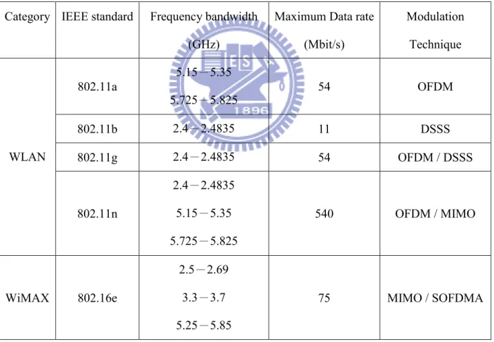
(11) Chapter 1 Introduction. Chapter 1. Introduction. 1.1 Background and Problems With the rapid adoption of wireless communication functionality in such products as personal computers, smart phones, and mobile internet devices (MID), the wireless local area network (WLAN) has played an important role in our daily life. Because of the need to increase the data rate, the WLAN standards including IEEE 802.11a/b/g/n were established to improve the wireless communication quality. The 802.11a WLAN standards operate from 5.15 to 5.35 GHz (5.2 GHz band) and 5.725 to 5.825 GHz (5.8 GHz band), and the 802.11b/g WLAN standards operate from 2.4 to 2.4835 GHz (2.4 GHz band). Furthermore, the 802.11n WLAN standards operate in the frequency range of both 802.11a (5.2 /5.8 GHz bands) and the 802.11b/g (2.4 GHz band).. For the concerned data rate, the 802.11a WLAN standard achieves a data rate up to 54 Mbps, while the 802.11b WLAN standard has a data rate up to 11 Mbps. Moreover, the 802.11g WLAN standard achieves a data rate up to 54 Mbps as the 802.11a. Because the Multi-input Multi-output (MIMO) technology is used in the 802.11n, the 802.11n WLAN standard can achieve a data rate up to 540 Mbps.. 1.
(12) Chapter 1 Introduction. Besides the WLAN systems, the new communication system of the Worldwide Interoperability for Microwave Access (WiMAX) which includes the 802.16 standards operating in the 2.5/3.5/5.5 GHz bands (2.5–2.69/3.3–3.7/5.25–5.85 GHz).. The WiMAX system is a long range communication system, which can deliver data stream with data rate up to 75 Mbps over 50 kilometers; in contrast, WLAN systems are limited to a maximum range of about 100 meters only. As the 802.11n WLAN standard, the WiMAX system also uses the MIMO technology to improve the communication performance.. Category IEEE standard. Frequency bandwidth. Maximum Data rate. Modulation. (GHz). (Mbit/s). Technique. 54. OFDM. 5.15-5.35 802.11a 5.725-5.825. WLAN. 802.11b. 2.4-2.4835. 11. DSSS. 802.11g. 2.4-2.4835. 54. OFDM / DSSS. 540. OFDM / MIMO. 75. MIMO / SOFDMA. 2.4-2.4835 802.11n. 5.15-5.35 5.725-5.825 2.5-2.69. WiMAX. 802.16e. 3.3-3.7 5.25-5.85. Table 1.1 Wireless communication systems.. 2.
(13) Chapter 1 Introduction. 1.2 Multi-input Multi-output (MIMO) Technology. Fig. 1.1 Multi-input Multi-output (MIMO) system.. In recent years, there is an increasing need for the use of wireless communication to transmit multimedia data streams. Therefore, we hope to attain higher data throughput, capacity, efficiency, and quality in the wireless communication systems. The Multi-input Multi-output (MIMO) technology uses multiple antennas at the transmitter and/or receiver to improve the communication performance, which offers a significant increase in the data throughput and/or the link range without requiring additional bandwidth or higher transmit power expenditure [1], [2].. The constitution of a MIMO system can be divided into three functions: multiplexing, diversity, and precoding. First of all, the multiplexing function splits a high data rate signal into multiple lower data rate streams and each data stream is transmitted from different. 3.
(14) Chapter 1 Introduction. transmit antenna in the same frequency channel. When the data streams arrive at the receiver antennas with adequately different spatial signatures, the receiver can separate these data streams and create parallel free channels. Secondly, the diversity function transmits a single data stream coded by using space-time coding techniques. It means that the data signal is emitted from each of the transmit antennas with completely or near orthogonal coding, and the diversity coding makes use of ideally independent fading in the multiple antenna links to enhance the signal diversity. Finally, the precoding function generalizes beamforming techniques to support the multi-layer transmission in the MIMO systems. In the precoding function, the multiple data streams of the signals are emitted from the transmit antennas with independent and appropriate phase weighting per each antenna such that the signal throughput is maximized at the receiver. Therefore, the benefits of precoding are to increase the signal gain from the constructive interference and to reduce the multipath fading effect.. Because the requirements for the wireless communication devices in modern time are light, slim, and small, the applicable space of these wireless terminal devices is compact and confined. If we use the MIMO system to enhance the transmitted signal performance and the data capacity, the mutual coupling between the multiple antennas has become more critical. Since the mutual coupling and high correlation are interrelated, the system throughput can deteriorate when there is high correlation between the propagation channels.. As mentioned above, the MIMO system often exploits the closely packed antennas in the confined space of wireless terminal devices. In order to solve the high mutual coupling between the multiple antennas, some decoupling techniques [3]-[8] are used to reduce the mutual coupling and correlation which, in turn, increase the system capacity and throughput. Further introductions and discussions about the various diversity techniques used in MIMO systems will be given in Chapter 2. 4.
(15) Chapter 1 Introduction. Throughput. multiplexing. diversity. precoding. Fading Protection. SINR. Fig. 1.2 Functions of MIMO system.. 1.3 Organization of Thesis The thesis is organized as follows: In Chapter 2, we describe various antenna diversity schemes and correlation coefficient for the MIMO system, and then we present the design of the proposed two-antenna MIMO system with a T-shaped slotline structure on the ground plane for reducing mutual coupling between the two antennas in Chapter 3. In Chapter 4, we discuss the Ansoft HFSS simulations and measured results with the two-port scattering parameters and far-field radiation patterns. Finally, we conclude this study and compare the pros and cons of the proposed antennas design and isolation structure in Chapter 5. 5.
(16) Chapter 2 Diversity Technology. Chapter 2. Diversity Technology. 2.1 Introduction The RF signal transmission between two antennas generally suffers from the power loss in space that affects performance evidently. The power loss between the transmitter and receiver is a result of three different phenomena: free-space attenuation, environmental fading, and atmospheric absorption.. First of all, due to the spherical TEM-wave nature of far fields radiated by an antenna, the free-space attenuation, which is also called path loss, accounts for the distance-square decrease of the power density. Path loss is a theoretical attenuation which occurs under free line-of-sight (LOS) conditions. If the transmission signal is far from the transmitter, the signal power density will decrease with increasing distance.. Secondly, the signal fading [9] is an attenuation that varies between a maximum and minimum value in an irregular way. The mobile devices sometimes move through areas with bad weather conditions and obstacles of various shapes and sizes, such as buildings, tunnels, and mountains, which can shadow and even completely cut off the transmission signals. The kind of shadowing effects will depend on the size of obstacles and on the distance to the. 6.
(17) Chapter 2 Diversity Technology. obstacles. Moreover, the received signal strength will unavoidably change and decrease. The type of signal fading is referred to as shadow fading [10]. For example, when the RF signals are transmitted in the outdoor propagation environment, the terrain types and weather conditions such as rainy days affect the quality of the transmission signal apparently. Therefore, the RF signals fade by the varied surrounding environment.. Finally, for the wireless long distance communication, the RF signals are reflected by the ionosphere to arrive at the receiver. Because the travelling paths of the signals pass through the atmosphere, parts of the signals are absorbed due to the molecules in the atmosphere of the earth. As a matter of fact, the atmospheric absorption is due to the electrons, molecules of various gases and water vapor. Furthermore, the wireless communications systems operating in the 60 GHz band contrarily take advantage of the high peak absorption caused by the oxygen, and in the transmission it does not interfere with other wireless communication system. It also has the high absorption in the 21 GHz band for the water vapor.. 2.2 Diversity Techniques As mentioned above, because of the power loss and signal fading between the transmitter and receiver, we may employ any of a number of diversity technologies for improving the reliability and quality of the transmission signals by using two or more communication channels with distinct characteristics. Moreover, the diversity technologies not only fight against channel interference and signal fading but also avoid error bursts.. 7.
(18) Chapter 2 Diversity Technology. There are many kinds of diversity schemes in the diversity technology. For example, the spatial diversity, angle diversity, frequency diversity, polarization diversity, pattern diversity and so on. Among these diversity schemes, only spatial diversity, polarization diversity and pattern diversity make for a practical implementation in the WLAN antenna systems.. In the next subsection, we present the different classes of diversity techniques and explain the relevant principles and basic methods.. 2.2.1 Spatial Diversity Spatial diversity makes use of multiple antennas with the same characteristics, which are spatially dispersed such that multi-path signals arriving at different antennas with different fading characteristics. Consequently, receiver can combine and demodulate these dissimilarly faded signals to extract the original transmission signals more accurately.. Depending upon the expected incidence of the transmission signal, the minimum spacing between the antennas in a wireless terminal required to achieve sufficiently low correlation between fading signals is usually about half wavelengths. As a matter of fact, we neglect the significant mutual coupling between the adjacent antennas for the ideal case. If the spacing between the nearby antennas is smaller than half wavelengths, other diversity techniques will be of more appeal [10].. However, in the practical implement we have to consider the intense mutual coupling effect for the closely placed antennas because the needs of mobile devices are compact and confinement. When we employ spatial diversity techniques to fight against the signal fading problem in the MIMO system, we also have to enhance the isolation between the antennas. 8.
(19) Chapter 2 Diversity Technology. In this thesis, two PIFA antennas are considered for operation at 2.4 GHz band. As will be shown later, a T-shaped slotline structure is used to reduce the mutual coupling between the two PIFA antennas.. 2.2.2 Angle Diversity Because the transmission signals are coming from distinct directions, for the independence of the signal fading variations the transmission signals can be used for angle or angular diversity, and angle diversity is a technique using multiple antenna beams to receive multipath signals arriving from different angles. In one word, angle diversity has the multi-beam characteristic to separate signal paths by their distinct angles of arrival.. For example, we can use two omnidirectional antennas in the indoor environment, and the transmission signals are reflected from different directions and angles because of the surrounding wall, ceiling, floor, and furniture. Two omnidirectional antennas also perform as the parasitical loading elements to each other and, thus, vary the antenna beams to control the reception of signals at distinct angles.. For angle diversity used in practice, it is effective and suitable for the obstacle-free environment, for example, omnidirectional antennas on a mobile terminal might not be a good idea, however, because of the field lobe blocked by the user.. 9.
(20) Chapter 2 Diversity Technology. 2.2.3 Frequency Diversity Frequency diversity depends on the fact that signal fades differently at dissimilar frequencies. In other words, fading characteristics are not correlated between two distinct frequency signals. Therefore, when one frequency signal fades, another may not.. Frequency diversity employs transmission of the identical signals at various frequency channels or spreading them over an extensive spectrum that is affected by selective frequency fading. It means the use of complementary transmission signals or multiple wireless systems operating cooperatively at different frequencies. This method can achieve distinct, independently-faded versions of the transmission signals. In the practical wireless applications, we make use of various managed wideband transmission channels with a guard band channel for automatic utilization by any fading channel. At the receiver, the RF circuits sense the signal-to-noise ratio (SNR) of the transmission signals and decide to select which is the best at any instant of time.. For example, Orthogonal Frequency Division Multiplexing (OFDM) modulation technique uses the digital multi-carrier modulation method. The transmission signals are divided into several orthogonal sub-carriers to deliver data. Because each sub-carrier only carry small partition of the transmission data, OFDM technique can take advantage of a low symbol rate, and the transmission signals avoid suffering from the multi-path fading or other environmental interference. In fact, we apply OFDM modulation technique to WLAN and WiMAX systems, and the transmission signal can preserve the entire data rates which are identical to the traditional single-carrier modulation technique in the same bandwidth.. 10.
(21) Chapter 2 Diversity Technology. However, the disadvantage of frequency diversity is the cost of operating multiple independent frequencies, and the cost is usually prohibitive. It is crucial and difficult to accomplish frequency management because frequency diversity has the challenge of generating several transmission signals and combining received signals of different frequencies in the meantime. Moreover, the intense mutual interference between the signal paths results in failing to manage the functions and characteristics of frequency diversity, and the available bandwidth is also restricted in practice.. 11.
(22) Chapter 3 The Proposed Microstrip-fed PIFA and T-shaped Slot Isolation Structure. Chapter 3. The Proposed Microstrip-fed PIFA and T-shaped Slot Isolation Structure. 3.1 Introduction When we want to accomplish higher data throughput, capacity, efficiency, and quality in the wireless communication systems, MIMO technology using multiple antennas at the transmitter and/or receiver may be employed. The diversity techniques are expected to reduce channel interference and signal fading and, thus, avoid data error bursts. Although the diversity techniques can fight against the signal fading and power loss between the transmitter and receiver, we also have to consider that the intense mutual coupling between the antennas is mainly due to the direct radiation coupling through the air and the current coupling through the ground plane, especially along the ground edge. The capacity of MIMO systems can also be shown to degrade if there are severe correlations due to the mutual coupling effect at the transmitter and/or receiver [11], [12]. Because the design in wireless mobile devices is limited to a reduced and restricted space, the antennas are placed closely and may result in serious mutual coupling. In this thesis, we consider the design of a pair of compact printed inverted-F antennas (PIFA) for operation at 2.4 GHz band and propose an isolation structure for suppressing mutual coupling through the ground plane. 12.
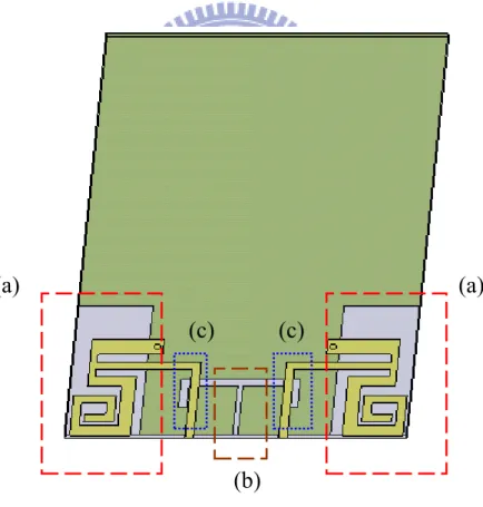
(23) Chapter 3 The Proposed Microstrip-fed PIFA and T-shaped Slot Isolation Structure. The structure proposed for investigation in this thesis is depicted in Fig. 3.1. The structure includes a pair of microstrip-fed PIFAs (Fig. 3.1(a)) and an isolation enhancement structure implemented on the ground plane. The main part of this novel structure is the T-shaped slotline junction (Fig. 3.1(b)). The vertical leg of the T-junction is open-ended at the edge of the ground plane. As one can see from region (c) of Fig. 3.1, before each of the two horizontal arms of the T-junction is short-ended, it crosses over the microstrip feed line of a PIFA. In this design, the two microstrip-to-slotline transitions provide coupling of energy between PIFAs and slotline T-junction which, when properly designed, can reduce the flow of current from one antenna to another through the ground plane and, thus, enhance the isolation between the two neighboring antennas. These are further discussed in the following sections.. (a). (a) (c). (c). (b) Fig. 3.1 Top view of the proposed design. (a) Microstrip-fed PIFA. (b) T-shaped slotline junction. (c) Microstrip-to-slotline transition. 13.
(24) Chapter 3 The Proposed Microstrip-fed PIFA and T-shaped Slot Isolation Structure. 3.2 Design and Configuration of PIFA 3.2.1 Development of PIFA To design the compact and practical antenna for wireless communication applications, the restricted space is an important issue. Therefore, in this thesis, we choose PIFA for the use with wireless mobile devices because of the merit of compact size and low cost. The development of PIFA originates from the half-wavelength dipole. For a center-fed half-wavelength dipole, the input impedance contains an inductive reactance. When the length of dipole is reduced to about 0.45 ~ 0.48 wavelength, depending on the conductor radius of dipole, the input impedance Zin = Rin ≈ 73 Ω is purely resistive. For such a resonant dipole, good input impedance matching is achieved with the 50-ohm or 75-ohm characteristic impedance of typical feed line (the return loss S11 is about -37 dB or -15 dB). When the length of dipole gets even shorter, the input impedance contains a capacitive reactance, which can greatly affect the performance of input impedance matching.. When the antenna miniaturization becomes an important factor or, in fact, a constraint of design, the first attempt to reduce the size is by replacing the half-wavelength dipole with quarter-wavelength monopole. Furthermore, by bending the straight wire of monopole into a horizontal wire as shown in Fig. 3.2(c), the antenna is vertical dimension shortened considerably, and the kind of antenna is called inverted-L antenna (ILA).. In order to further reduce the length of inverted-L antenna, the input impedance contains a capacitive reactance which, just as the center-fed dipole, affects the performance of impedance matching.. 14.
(25) Chapter 3 The Proposed Microstrip-fed PIFA and T-shaped Slot Isolation Structure. (a) Center-fed, half-wavelength dipole.. (b) Coaxial cable-fed monopole.. (c) Inverted-L antenna (ILA).. (d) Inverted-F antenna (IFA). Fig. 3.2 The development of inverted-F antenna.. 15.
(26) Chapter 3 The Proposed Microstrip-fed PIFA and T-shaped Slot Isolation Structure. Fig. 3.2(d) shows the improved inverted-F antenna (IFA) for the inverted-L antenna. Moreover, for the length of ILA smaller than quarter-wavelength, we just add a loop inductor behind the center-fed point of ILA to compensate the input capacitive reactance. This kind of revised design can achieve better performance of input impedance matching and radiation efficiency with antenna occupying only a small volume.. 3.2.2 Design of The Proposed Microstrip-fed PIFA Fig. 3.3 shows the structure of the proposed PIFA for use with wireless mobile applications. Because the length of the open-ended transmission line is long, the entire size of PIFA is too large to occupy the space allowed in typical wireless mobile devices. To reduce the size of PIFA to meet the board size constraint, we simply convert the straight open-ended transmission line into a spiral.. By making the straight line into a spiral, an additional inductive loading effect is introduced. Although the design has dual-band property, we focus on the reduced antenna size.. Fig. 3.3 Structure of the proposed PIFA. 16.
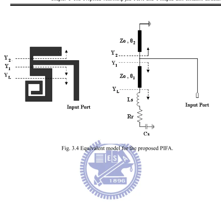
(27) Chapter 3 The Proposed Microstrip-fed PIFA and T-shaped Slot Isolation Structure. An equivalent circuit model [13] for the spiraled PIFA is established as shown in Fig. 3.4. As mentioned previously, the PIFA is the open-circuited transmission line at one end in shunt with the short-circuited transmission line at the other end in order to compensate the reactance. However, because the spiral open-ended transmission line has an inductive effect, we have to consider the parasitic inductor in the open end.. The short end of PIFA is equivalent to the short-circuited transmission line of length θ 2 , and the characteristic impedance is Z 0 . The input admittance seen looking toward the short end is Y2 . On the other hand, the open end of PIFA is originally equivalent to the open-circuited transmission line of length θ1 loaded by an effective radiation resistance Rr , and the characteristic impedance is Z 0 , but a parasitic inductor Ls is inserted in the end of the open-circuited transmission line, and a parasitic capacitor C s is shunted to ground for the fringe fields.. Yin = Y1 + Y2 = Y0. YL + jY0 tan θ1 − jY0 cot θ 2 Y0 + jYL tan θ1. (3-1). where. YL = Z. −1 L. 1 = jωLS + Rr + jωC S . −1. (3-2). and the input reflection coefficient Γin is. 1 1 − Z − Z 0 Yin Y0 Y0 − Yin Γin = in = = 1 1 Y0 + Yin Z in + Z 0 + Yin Y0 17. (3-3).
(28) Chapter 3 The Proposed Microstrip-fed PIFA and T-shaped Slot Isolation Structure. Fig. 3.4 Equivalent model for the proposed PIFA.. 3.3 Design of The T-shaped Slot Isolation Structure After we present the proposed microstrip-fed PIFA, the second part of the designed circuit is the T-shaped slot isolation structure, which is composed of short-ended and open-ended slotline as shown in Fig. 3.5. Located in the lower center region of the ground plane, the T-shaped slotline is a symmetric structure so the entire two-port circuit is ideally reciprocal. Moreover, because the merit of this isolation structure is low-cost and easy to be fabricated, it can be widely used in the wireless mobile devices.. 18.
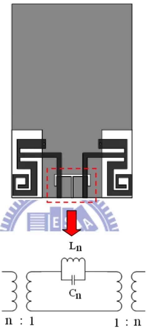
(29) Chapter 3 The Proposed Microstrip-fed PIFA and T-shaped Slot Isolation Structure. Symmetric plane. Short-ended slotline. Short-ended slotline. Open-ended slotline Fig. 3.5 The proposed T-shaped slot isolation structure.. The T-shaped slotline in Fig. 3.5 consists of an open-ended slotline shunted with two short-ended slotline. Because the electric lengths of the open-ended and short-ended slotline are smaller than λs/ 4, the T-shaped slotline can be modeled as a parallel inductor Ln and capacitor Cn [14], [15] as shown in Fig. 3.6. The designed values of the inductor and capacitor are selected by length and width of the open-ended and short-ended slotline. When we want to design the isolation structure for a specific frequency band, the length and width of the slotline can be tuned to fit the desired values of the inductor and capacitor.. 19.
(30) Chapter 3 The Proposed Microstrip-fed PIFA and T-shaped Slot Isolation Structure. The equivalent circuit for the parallel open-ended and short-ended slotline is shown in Fig. 3.6, and the following computations show that the circuit of parallel inductor and capacitor is open at the resonant frequency.. Fig. 3.6 Equivalent circuit for the T-shaped slotline junction.. Zn =. ωn =. 1 1 1 + 1 jωLn jω C n. 1. =. jωLn 1 − ω 2 Ln C n. (3.4). (3.5). Ln C n. 20.
(31) Chapter 3 The Proposed Microstrip-fed PIFA and T-shaped Slot Isolation Structure. jLn Z n (ω = ω n ) =. Ln C n 1 1− ( ) 2 Ln C n Ln C n. →∞. (3.6). 3.4 Microstrip-to-slotline Transition. Fig. 3.7 Microstrip-to-slotline transition.. A transmission line equivalent circuit of the transition shown in Fig. 3.7 was proposed by Chambers et al. [16] and is shown here in Fig. 3.8. The reactance X 0 s represents the inductance of a shorted slot, and C 0c is the capacitance of an open microstrip. Z 0 s and Z 0 m are the slot and microstrip characteristic impedance, respectively. θ s and θ m represent the electrical lengths (quarter-wave at the center frequency) of the extended portions of the slot and the microstrip, respectively, measured from the reference planes as shown in Fig. 3.7. The transformer turns ratio n represents the magnitude of the coupling between the microstrip and slot. 21.
(32) Chapter 3 The Proposed Microstrip-fed PIFA and T-shaped Slot Isolation Structure. Fig. 3.8 Transmission line equivalent circuit for the transition.. Fig. 3.9 Reduced equivalent circuit.. Fig. 3.10 Transformed equivalent circuit.. 22.
(33) Chapter 3 The Proposed Microstrip-fed PIFA and T-shaped Slot Isolation Structure. For further analysis the equivalent circuit in Fig. 3.8 may be redrawn as in Fig. 3.9. Here,. jX s = Z 0 s. jX 0 s + jZ 0 s tan θ s Z 0 S − X 0 s tan θ s. (3.7). and. jX m = Z 0 m. 1 jωC0 c + jZ 0 m tan θ m Z 0 m + tan θ m ωC0c. (3.8). After transformation to the microstrip side, the equivalent circuit of Fig. 3.9 reduces to that shown in Fig. 3.10. In this circuit,. ZS =. =. 1 1 1 + jX s Z 0 s. (3.9). 2 s. 2 0s. Z 0s X Z Xs + j 2 2 2 Z 0s + X s Z 0 s + X s2. and Z 0 s X s2 Z 02s + X s2. (3.10). Z 02s X s X =n 2 Z 0 s + X s2. (3.11). R = n2. 2. Finally, the reflection coefficient Γ is given by. Γ=. R − Z0m + j( X m + X ) R + Z0m + j ( X m + X ). (3.12). From the above analysis, we can determine the characteristic impedance of the slot Z 0 s to match the microstrip line impedance Z 0 m .. 23.
(34) Chapter 3 The Proposed Microstrip-fed PIFA and T-shaped Slot Isolation Structure. In the approximate analysis reported by Knorr [17] the transformer turns ratio n is determined from a knowledge of the slotline field components as. n=. V ( h) V0. (3.13). b/2. V ( h) = −. ∫E. y. (h) dy. (3.14). −b / 2. V0 is the voltage across the slot and E y (h) is the electric field of the slotline on the other surface of the dielectric substrate and they may be written as. E y ( h) = −. where. q0 =. 2π u. λ0. u = [ε r − (. V0 2πu 2πu {cos h − cot q 0 sin h} λ0 λ0 b. (3.15). h + tan −1 (u / v). (3.16). λ0 2 12 ) ] λs. v = [(. 1 λ0 2 ) − 1] 2 λs. (3.17). the ratio of the phase velocity v to the group velocity vg is related to the sensitivity of λs λ0 with respect to frequency f, it is given by. v f ∆ (λ s λ0 ) = 1− λ s λ0 vg ∆f. 24. (3.18).
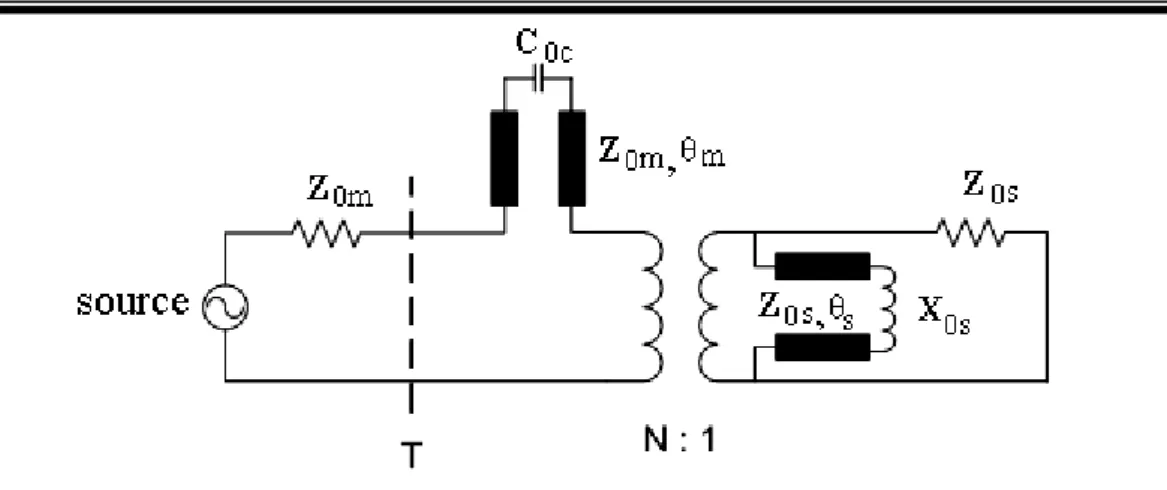
(35) Chapter 3 The Proposed Microstrip-fed PIFA and T-shaped Slot Isolation Structure. 3.5 Discussion of The Two-Port Network Model Combining the results of section 3.2.2, section 3.3, and section 3.4, the two-port network model is shown in Fig. 3.11. The most important concept is that the entire circuit consists of a pair of microstrip-fed PIFAs and a T-shaped slot isolation structure, and the signal coupling between two PIFAs and T-shaped slotline is accomplished by a pair of microstrip-to-slotline transitions shown as the transformers in Fig. 3.11. Therefore, although the middle circuit of parallel inductor Ln and capacitor Cn is open to lower the coupling between two ports at resonant frequency, the backward coupling signal through the transformer is weak, thus, it can affect the original impedance-matching characteristic of PIFA only slightly.. Fig. 3.11 Two-port network model. 25.
(36) Chapter 3 The Proposed Microstrip-fed PIFA and T-shaped Slot Isolation Structure. For the analysis of designed parameters, we should find the closed-form expressions for slotline wavelength and impedance. There are different kinds of utilization for the high or low value of relative permittivity ε r , for example, high ε r substrates are used for circuit applications to confine the field near the slot. On the other hand, slotlines on low ε r substrates have interesting applications in antennas. In this thesis, we use low ε r substrate to design PIFA and T-shaped slotline. As mentioned above, the closed-form expressions for slotline wavelength and impedance are the key factors for analyzing the designed circuit, and Janaswamy and Schaubert [18] have acquired closed-form expressions for low ε r substrates by curve fitting the numerical results obtained from the method of Fourier-transform domain (FTD). These expressions are as follows and are valid for the range of parameters [18].. From the fabricated circuit board, we know the designed relative permittivity ε r , substrate thickness h, and the width W of slotline. The other considered parameter is free-space wavelength λ0 for the operating frequency. With the designed values of circuit parameters, we can firstly check the range of these variables for the conditions (3.19) of closed-form expressions, and after satisfying the premise, the closed-form expressions for slotline wavelength and impedance are given respectively as follows:. 2.22 ≤ ε r ≤ 9.8 0.0015 ≤. W. 0.006 ≤. h. λ0 λ0. ≤ 1.0 ≤ 0.06. 26. (3.19).
(37) Chapter 3 The Proposed Microstrip-fed PIFA and T-shaped Slot Isolation Structure. For 0.0015 ≤. W. λ0. ≤ 0.075 and 3.8 ≤ ε r ≤ 9.8. λs εr W = 0.9217 − 0.277 ln ε r + 0.0322( ) h (W + 0.435) λ0 h . 1. 2. (3.20). h 3.65 − 0.01ln( ) 4.6 − λ0 ε r2 W λ (9.06 − 100W λ ) 0 0 av = 0.6 %, |max| = 3 % (at three points, occurs for. Z os = 73.6 − 2.15ε r + (638.9 − 31.37ε r )(. W. λ0. W > 1 and ε r > 6 ) h. ) 0.6. W. h (W + 0.876ε r − 2) h W h + 0.51(ε r + 2.12)( ) ln(100 ) λ0 h + (36.23 ε r + 41 − 225) 2. h − 0.753ε r. (3.21). λ0. W. λ0. av = 1.58 %, max = 5.4 % (at three points, occurs for. W > 1.67 ) h. For the fixed relative permittivity ε r , substrate thickness h, and free-space wavelength. λ0 , we can infer the relation between slotline width and frequency from observing the closed-form expressions for slotline impedance Z 0 s , and the relations are shown below.. 27.
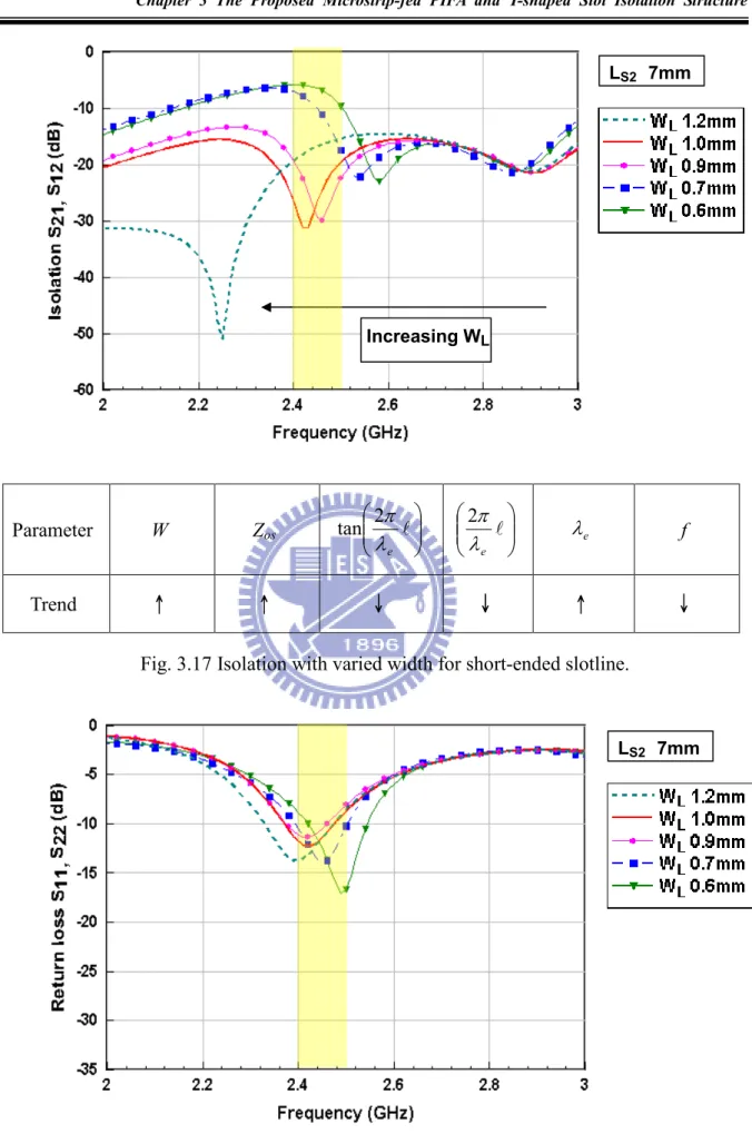
(38) Chapter 3 The Proposed Microstrip-fed PIFA and T-shaped Slot Isolation Structure. Short - ended slotline (Inductor) :. Z in , short = jZ 0 s tan( β l) =. Open - ended slotline (Capacitor) : Z in ,open. For the fixed Z in , short ⇒ W ∝ Z os ∝. For the fixed Z in ,open. 2π jZ 0 s tan λe. 2π = - jZ 0 s cot( β l) = − jZ 0 s cot λe. 1. ∝. l . l . (3.22). 1 1 ∝ 1 f. 2π tan l λe λe 1 1 ⇒ W ∝ Z os ∝ ∝ ∝ f 2π λe cot l λ e . (3.23). (3.22) indicates the input impedances of short-ended and open-ended slotline, and from the positive or negative reactance, we can determine whether the input impedance of slotline is inductive or capacitive. When the positive and negative reactances are equal, the parallel circuit is open at resonant frequency f n ; in order to maintain the equal state, the input impedances Z in , short and Z in ,open of slotline must keep the same. Besides, we also know the characteristic impedance Z 0 s of slotline is proportional to the varied slotline width W from (3.21). However, for the fixed input impedances, the characteristic impedance Z 0 s is 2π inversely proportional to tan λ e. 2π l and cot λe . l . After some mathematical simplification, . we finally can infer that the slotline width W is inversely proportional to the resonant frequency f n for short-ended slotline. On the other hand, the slotline width W is proportional to the resonant frequency f n for open-ended slotline.. 28.
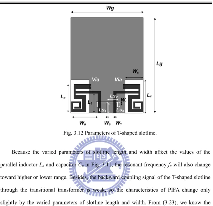
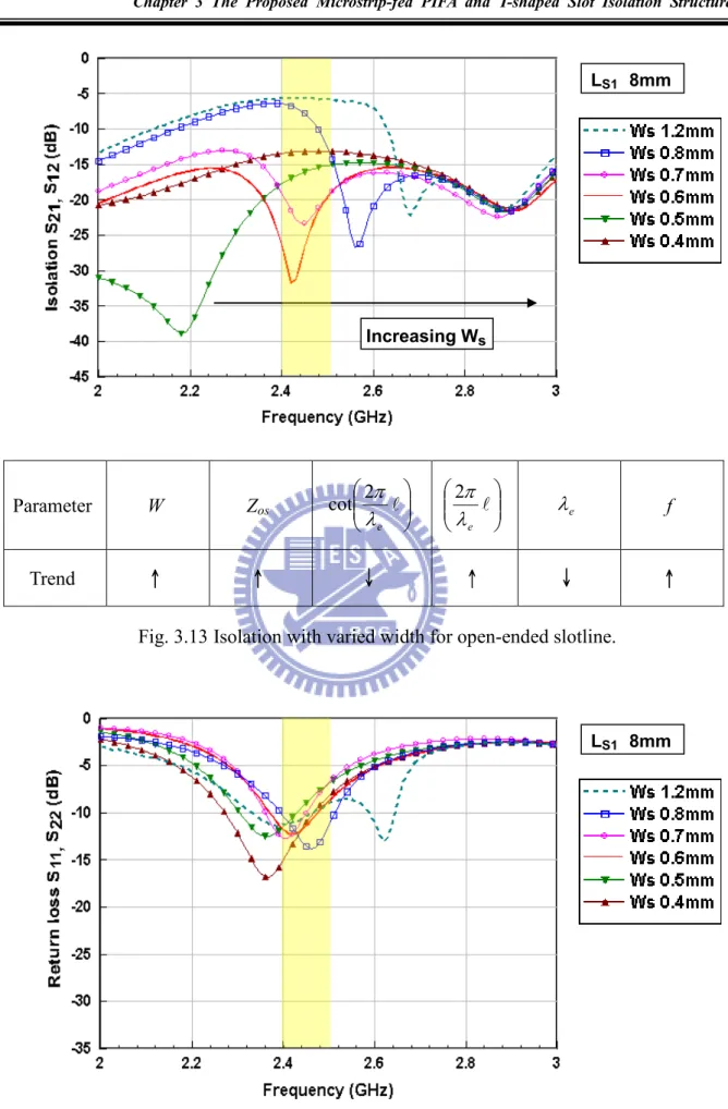
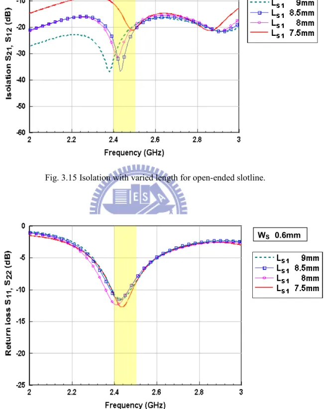
(39) Chapter 3 The Proposed Microstrip-fed PIFA and T-shaped Slot Isolation Structure. Fig. 3.12 Parameters of T-shaped slotline. Because the varied parameters of slotline length and width affect the values of the parallel inductor Ln and capacitor Cn in Fig. 3.11, the resonant frequency fn will also change toward higher or lower range. Besides, the backward coupling signal of the T-shaped slotline through the transitional transformer is weak, so the characteristics of PIFA change only slightly by the varied parameters of slotline length and width. From (3.23), we know the relations between slotline width and frequency. Therefore, Fig. 3.13 and Fig. 3.17 show the isolation with varied width for open-ended and short-ended slotline respectively, and the trends of resonant frequency change greatly with little varied slotline width. Although the isolation for open-ended and short-ended slotline alters intensively, the return loss still covers the 2.4 GHz band as shown in Fig. 3.14 and Fig. 3.18. Furthermore, Fig. 3.15 and Fig. 3.19 also show the isolation with varied length for open-ended and short-ended slotline respectively. However, due to the tiny extent of changed electrical length, the isolation has little frequency-shifted phenomenon, and the return loss almost stays the same as shown in Fig. 3.16 and Fig. 3.20.. 29.
(40) Chapter 3 The Proposed Microstrip-fed PIFA and T-shaped Slot Isolation Structure. LS1 8mm. Increasing Ws. Parameter. W. Zos. 2π cot λe. Trend. ↑. ↑. ↓. l . 2π λe. l . ↑. λe. f. ↓. ↑. Fig. 3.13 Isolation with varied width for open-ended slotline.. LS1 8mm. Fig. 3.14 Return loss with varied width for open-ended slotline. 30.
(41) Chapter 3 The Proposed Microstrip-fed PIFA and T-shaped Slot Isolation Structure. WS 0.6mm. Fig. 3.15 Isolation with varied length for open-ended slotline.. WS 0.6mm. Fig. 3.16 Return loss with varied length for open-ended slotline.. 31.
(42) Chapter 3 The Proposed Microstrip-fed PIFA and T-shaped Slot Isolation Structure. LS2 7mm. Increasing WL. Parameter. W. Zos. 2π tan λe. Trend. ↑. ↑. ↓. l . 2π λe. l . ↓. λe. f. ↑. ↓. Fig. 3.17 Isolation with varied width for short-ended slotline.. LS2 7mm. Fig. 3.18 Return loss with varied width for short-ended slotline. 32.
(43) Chapter 3 The Proposed Microstrip-fed PIFA and T-shaped Slot Isolation Structure. WL 1mm. Fig. 3.19 Isolation with varied length for short-ended slotline.. WL 1mm. Fig. 3.20 Return loss with varied length for short-ended slotline.. 33.
(44) Chapter 4 The Simulated and Measured Results. Chapter 4. The Simulated and Measured Results. 4.1 The Fabricated Test Structures Two test boards were fabricated in this study. They have the same PIFAs. To test the effectiveness of the proposed isolation structure, one board has a solid ground plane while another board has a specific T-shaped slot structure etched out of its ground plane.. The proposed circuit is designed on the printed circuit board for operation at 2.4 GHz band, and the dimensions of the circuit board are selected to be 60 mm in length and 40 mm in width. The entire size is suitable for wireless mobile devices. The circuit board is fabricated with a 0.8-mm-thick FR-4 substrate of relative permittivity 4.4 and loss tangent 0.02. The conductive copper on the FR-4 substrate has a conductivity of 5.8×10⁷S/m. Both PIFAs are fed by 50 Ω microstrip lines which are further coupled through the T-shaped slotline structure on the ground plane to facilitate a mutual-coupling-cancelling signal. The detailed substrate parameters are listed in Table 4.1.. 34.
(45) Chapter 4 The Simulated and Measured Results. Material. Fr-4. Substrate. *Conductor. Relative. Loss tangent. Conductivity. thickness (h). thickness (t). permittivity(ε r ). (tanδ). (σ). 0.8 mm. 0.035 mm. 4.4. 0.02. 5.8×10⁷ S/m. Table 4.1 Substrate Parameters.. *Conductor thickness:. The specification of the conductor thickness is given as “copper foil 1 oz,” which means 1 oz of copper occupying an area of 1 ft2. Since the density of copper is 8.9 g / cm3, the following computation yields a foil thickness of 35 um.. 1oz = 28.35 g. (4-1 a). 1 ft = 304.8 mm. 1oz 28.35 g = = 3.0516 ⋅ 10 −4 ( g ) 2 2 2 mm 2 ft 304.8 mm −4 g 8.9 ⋅10 −3 ( g ) 3 ) × t ( mm ) = 3.0516 ⋅ 10 ( mm mm 2 ⇒ t ≈ 35( µm) = 0.035( mm). (4-1 b). Fig. 4.1 shows the geometry of the proposed PIFA and T-shaped slot structure for use with wireless mobile applications. Because the straight length of the open-ended transmission line is long, the entire size of PIFA is too large to occupy the space in the wireless mobile devices. To reduce the size of PIFA to meet the board size constraint, we simply convert the straight open-ended transmission into a spiral.. 35.
(46) Chapter 4 The Simulated and Measured Results. Besides, the T-shaped slot structure is located between two PIFAs on the ground plane, and the dimensions of the PIFA and T-shaped slotline are also shown in Table. 4.2.. Fig. 4.1 Geometry of the proposed design.. Lg. Wg. Lc. Wc. La. Wa. Wd. 60. 40. 18.5. 8.8. 13.8. 13.5. 10. L1. W1. Ws. Ls1. Ls2. Ls3. WL. 10. 1. 0.6. 8. 7. 4. 1. Table 4.2 Design Parameters (Unit: mm). 36.
(47) Chapter 4 The Simulated and Measured Results. 4.2 Two-Port Scattering Parameters Fig. 4.2 shows the top-view photograph of the fabricated antenna without the isolation slot, for which dimensions of the circuit board are 60 mm in length and 40 mm in width. The bottom view of the fabricated antenna is shown in Fig. 4.3.. Fig. 4.2 Photograph of the fabricated antenna without the slot (top view).. Fig. 4.3 Photograph of the fabricated antenna without the slot (bottom view). 37.
(48) Chapter 4 The Simulated and Measured Results. Fig. 4.4 shows the top-view photograph of the fabricated antenna with the isolation slot. Finally, we can clearly observe the entire isolation enhancement structure on the underside of the fabricated board shown in Fig. 4.5.. Fig. 4.4 Photograph of the fabricated antenna with the slot (top view).. Fig. 4.5 Photograph of the fabricated antenna with the slot (bottom view). 38.
(49) Chapter 4 The Simulated and Measured Results. The two-port scattering parameters show the performance of the return loss (S11, S22) and isolation (S12, S21). The PIFA is designed for the applications of wireless local area network (WLAN) at the 2.4-GHz band. We design the PIFA for the two cases: without and with the T-shaped slot structure on the ground plane. The HFSS simulated results of the return loss and isolation for the PIFA without the T-shaped slot structure are shown in Fig. 4.6. The return loss has good performance below -10 dB, but the isolation is poor because of the intense mutual coupling between the antennas. Moreover, the measured return loss shown in Fig. 4.7 is similar to the HFSS simulated results, and the measured isolation is better than the simulated results. Because the actual environment for the measurement is not as ideal as the free-space surrounding assumed in HFSS simulation, a perfect match between measured and simulated results shouldn’t be expected. The detailed comparison of simulated and measured results is shown in Fig. 4.8.. Fig. 4.6 HFSS simulated results without slot.. 39.
(50) Chapter 4 The Simulated and Measured Results. Fig. 4.7 Measured results without slot.. Fig. 4.8 The comparison of the simulated and measured results without slot. 40.
(51) Chapter 4 The Simulated and Measured Results. Next, by employing the T-shaped slot structure, HFSS simulated results shown in Fig. 4.9 clearly indicate that while the performance of return loss remains almost unchanged, the previously observed mutual coupling peaks have become deep nulls at around 2.4GHz. These are confirmed by the measured results shown in Fig. 4.10. The detailed comparison of simulated and measured results is shown in Fig. 4.11. In summary, the simulated and measured results prove that the proposed T-shaped slot structure does enhance the isolation between two nearby PIFAs. It is not only low-cost but also easy to be fabricated.. Fig. 4.9 HFSS simulated results with slot.. 41.
(52) Chapter 4 The Simulated and Measured Results. Fig. 4.10 Measured results with slot.. Fig. 4.11 The comparison of simulated and measured results with slot. 42.
(53) Chapter 4 The Simulated and Measured Results. 4.3 Far-Field Radiation Patterns Fig. 4.12, Fig. 4.13, and Fig. 4.14 show respectively the measured Eθ radiation patterns in the X-Y, X-Z, and Y-Z planes both with and without T-shaped slot structure; the corresponding measured Eφ radiation patterns are shown in Figs. 4.15-4.17 while Table 4.3 summaries the peak gain data.. As will be shown in section 4.4, the T-shaped slot structure changes the current distribution on the ground plane. As a result, changes in radiation patterns and peak gains are expected, and apparently the presence of the T-shaped slot structure result in slightly lower peak gains in all these planes.. Type. Plane. X-Y. X-Z. Y-Z. -0.1. -1.8. -0.6. -0.7. -2.1. -1.3. -0.6. -0.3. -0.7. PIFA without T-shaped slot structure. PIFA with T-shaped slot structure. Difference. Table 4.3 Peak Gain (Unit: dBi).. 43.
(54) Chapter 4 The Simulated and Measured Results. Fig. 4.12 E-theta radiation patterns with and without slot in the X-Y plane.. 44.
(55) Chapter 4 The Simulated and Measured Results. Fig. 4.13 E-theta radiation patterns with and without slot in the X-Z plane.. Fig. 4.14 E-theta radiation patterns with and without slot in the Y-Z plane. 45.
(56) Chapter 4 The Simulated and Measured Results. Fig. 4.15 E-phi radiation patterns with and without slot in the X-Y plane.. Fig. 4.16 E-phi radiation patterns with and without slot in the X-Z plane. 46.
(57) Chapter 4 The Simulated and Measured Results. Fig. 4.17 E-phi radiation patterns with and without slot in the Y-Z plane.. 47.
(58) Chapter 4 The Simulated and Measured Results. 4.4 Surface Current Distribution. (a) without the T-shaped slot structure. (b) with the T-shaped slot structure. Fig. 4.18 Surface current distribution of the PIFAs and top ground plane at 2.45 GHz.. Fig. 4.18 shows the surface current distribution of the PIFAs and the upper side of the ground plane, and we can clearly observe that the T-shaped slot structure isolates the surface current at the edge and. the middle area of ground plane. Moreover, the major parts of the. source signal distribute over the PIFA and the areas around the two ground vias.. 48.
(59) Chapter 4 The Simulated and Measured Results. (a) without the T-shaped slot structure. (b) with the T-shaped slot structure. Fig. 4.19 Surface current distribution of the top ground plane at 2.45 GHz.. Because a finite-sized ground plane with non-zero thickness is considered in the HFSS simulation, current will flow on both sides of the ground plane. Figs. 4.19 and 4.20 respectively show the surface current distribution on the top and bottom side of the ground plane at 2.45 GHz. As expected, each PIFA's ground via and microstrip feed line cause the return current to remain mostly on the upper side of the ground plane. On the other hand, the smaller surface current observed on the lower side of the ground plane is due to the field fringing effects associated with a finite-sized ground plane. 49.
(60) Chapter 4 The Simulated and Measured Results. (a) without the T-shaped slot structure. (b) with the T-shaped slot structure. Fig. 4.20 Surface current distribution of the bottom ground plane at 2.45 GHz.. 50.
(61) Chapter 5 Conclusion. Chapter 5. Conclusion. A novel isolation structure based on a T-shaped slotline junction for use with diversity-capable wireless communication systems has been presented. The entire circuit is composed of a pair of compact microstrip-fed PIFAs, a pair of microstrip-to-slotline transitions, and a T-shaped slotline junction implemented on the ground plane. A spiral open-ended transmission line design is employed for reducing the size of PIFA, which makes it compact and practical for use with wireless mobile devices. For the two PIFAs placed in close proximity, an intense mutual coupling is inevitable. A T-shaped slot structure is proposed in this thesis as an isolation enhancement structure to diminish the coupling effect.. To validate the effectiveness of the proposed isolation enhancement scheme, two test boards are fabricated. Although the T-shaped slotline is located between two PIFAs to reduce the strong mutual coupling, two PIFAs still maintain the original impedance matching characteristics. Furthermore, we also prove the fact that T-shaped slotline increases the isolation without affecting the performance of PIFA by HFSS simulated and measured results, which include two-port scattering parameters, radiation patterns, and surface current distribution.. 51.
(62) References. References. [1] G. J. Foschini, “Layered space-time architecture for wireless communication in a fading environment when using multi-element antennas,” Bell Labs Tech J., vol. 1, no. 2, pp. 41–59, 1996. [2] J. W.Wallace, M. A. Jensen, A. L. Swindlehurst, and B. D. Jeffs, “Experimental characterization of the MIMO wireless channel: Data acquisition and analysis,” IEEE Trans. Wireless Commun., vol. 2, pp.335–343, Mar. 2003. [3] D. Sievenpiper, L. Zhang, R. F. J. Broas, N. G. Alexopolous, and E. Yablonovitch, “High-impedance electromagnetic surfaces with a forbidden frequency band,” IEEE Microw. Theory Tech., vol. 47, no. 11, pp. 2059–2074, Nov. 1999. [4] F. Yang and Y. Rahmat-Samii, “Microstrip antennas integrated with electromagnetic band-gap (EBG) structures: A low mutual coupling design for array applications,” IEEE Trans. Antennas Propag., vol. 51, no. 10, pp. 2936–2946, Oct. 2003. [5] L. Li, B. Li, H. X. Liu, and C. H. Liang, “Locally resonant cavity cell model for electromagnetic band gap structures,” IEEE Trans. Antennas Propag., vol. 54, no. 1, pp. 90–100, Jan. 2006. [6] Choi, V. Govind, and M. Swaminathan, “A novel electromagnetic bandgap (EBG) structure for mixed-signal system applications,” in Proc. IEEE Radio and Wireless Conf., Sep. 19–22, 2004, pp. 243–246.. 52.
(63) References. [7] C.-Y. Chiu, C.-H. Cheng, R. D. Murch, and C. R. Rowell, “Reduction of mutual coupling between closely-packed antenna elements,” IEEE Trans. Antennas Propag., vol. 55, no. 6, pp. 1732–1738, Jun. 2007. [8] D. Guha, M. Biswas, and Y. M. M. Antar, “Microstrip patch antenna with defected ground structure for cross polarization suppression,” in IEEE Antennas Wireless Propag. Lett., 2005, vol. 4, pp. 455–458. [9] G. J. Foschini and M. J. Gans, “On limits of wireless communications in a fading environment when using multiple antennas,” Wireless Personal Communications, vol. 6, pp. 311–335, March 1998. [10] Young P.H., Electronic Communication Techniques, 4th edition, Prentice Hall, 1999. [11] D. Shiu, G. J. Foschini, M. J. Gans, and J. M. Kahn, “Fading correlation and its effect on the capacity of multi-element antenna systems,” IEEE Trans. Comm., vol. 48, pp. 502–513, March 2000. [12] D. Gesbert, H. B¨olcskei, D. Gore, and A. Paulraj, “Outdoor MIMO wireless channels: Models and performance prediction,” IEEE Trans. Communications, vol. 50, pp. 1926–1934, Dec. 2002. [13] Y.-S. Wang, M.-C. Lee, and S.-J. Chung, “Two PIFA-Related Miniaturized Dual-Band Antennas,” IEEE Trans. Antennas Propag., vol. 55, no. 3, pp. 805–811, March 2007. [14] D. Ahn, J. S. Park, C. S. Kim, J. Kim, Y. Qian, and T. Itoh, “A design of the low-pass filter using the novel microstrip defected ground structure,” IEEE Microw. Theory Tech., vol. 49, no. 1, pp. 86–93, Jan. 2001. [15] C. Caloz, H. Okabe, T. Iwai, and T. Itoh, “A simple and accurate model for microstrip structures with slotted ground plane,” IEEE Microwave Wireless Comp. Lett., vol. 14, no. 4, pp. 133–135, Apr. 2004.. 53.
(64) References. [16] Chamber, D., et al., “Microwave Active Network Synthesis,” Semiannual Report, Stanford Resr. Inst., June 1970. [17] Knorr, J. B., “Slotline Transitions,” IEEE Trans., Vol. MTT-22, 1974, pp. 548-554. [18] Janaswamy, R., and D. H. Schaubert, “Characteristic Impedance of a Wide Slotline on Low Permittivity Substrates,” IEEE Trans., Vol. MTT-34, 1986, pp. 900-902.. 54.
(65)
數據

+7
Outline
相關文件
The Secondary Education Curriculum Guide (SECG) is prepared by the Curriculum Development Council (CDC) to advise secondary schools on how to sustain the Learning to
好了既然 Z[x] 中的 ideal 不一定是 principle ideal 那麼我們就不能學 Proposition 7.2.11 的方法得到 Z[x] 中的 irreducible element 就是 prime element 了..
volume suppressed mass: (TeV) 2 /M P ∼ 10 −4 eV → mm range can be experimentally tested for any number of extra dimensions - Light U(1) gauge bosons: no derivative couplings. =>
For pedagogical purposes, let us start consideration from a simple one-dimensional (1D) system, where electrons are confined to a chain parallel to the x axis. As it is well known
Define instead the imaginary.. potential, magnetic field, lattice…) Dirac-BdG Hamiltonian:. with small, and matrix
incapable to extract any quantities from QCD, nor to tackle the most interesting physics, namely, the spontaneously chiral symmetry breaking and the color confinement..
• Formation of massive primordial stars as origin of objects in the early universe. • Supernova explosions might be visible to the most
All steps, except Step 3 below for computing the residual vector r (k) , of Iterative Refinement are performed in the t-digit arithmetic... of precision t.. OUTPUT approx. exceeded’
