國 立 交 通 大 學
電子工程學系 電子研究所碩士班
碩 士 論 文
三閘極金氧半場效電晶體利用基極偏壓
調變臨界電壓之分析與模型建立
Investigation and Modeling of Threshold-Voltage Modulation
through Substrate Bias for Tri-gate MOSFETs
研 究 生:江俊賢
指導教授:蘇 彬 教授
三閘極金氧半場效電晶體利用基極偏壓
調變臨界電壓之分析與模型建立
Investigation and Modeling of Threshold-Voltage Modulation
through Substrate Bias for Tri-gate MOSFETs
研 究 生:江俊賢 Student: Chun-Hsien Chiang
指導教授:蘇 彬 Advisor: Pin Su
.
國 立 交 通 大 學
電子工程學系 電子研究所
碩 士 論 文
A Thesis
Submitted to Department of Electronics Engineering & Institute of Electronics College of Electrical and Computer Engineering
National Chiao Tung University in Partial Fulfillment of the requirements
for the Degree of Master in
Electronic Engineering
August 2012
Hsinchu, Taiwan, Republic of China
I
三閘極金氧半場效電晶體利用基極偏壓調變臨界電壓
之分析與模型建立
研究生:江俊賢 指導教授:蘇 彬 博士
國立交通大學 電子工程學系
電 子 研 究 所 碩 士 班
摘 要
本論文探討三閘極金氧半場效電晶體藉由基極偏壓調變臨界電壓的可行 性 。 我 們 利 用 三 維 原 子 等 級 模 擬 探 討 隨 機 參 雜 濃 度 變 動 (Random Dopant Fluctuation)對於 BULK 三閘極元件中 Punch-Through-Stopper (PTS)區域的影響。 我們的研究發現藉由高濃度摻雜的 PTS 區域雖能有效的幫助基極偏壓調變元件 的臨界電壓,但同時也造成額外 Bulk 三閘極電晶體的元件變異。因此,在比較 BULK 以及 SOI 三閘極元件的變異度時,上述效應的影響應該要納入考量。 由於 bulk 三閘極元件中 PTS 區域會引起額外的元件變異,因此利用基極電 壓來調變 SOI 三閘極元件結構的臨界電壓似乎是個較佳的選項。為了有利於 SOI 三閘極元件多重臨界電壓的設計,我們準確地推導了具有高度深埋氧化層(BOX) 厚度微縮性的次臨界解析模型。利用此模型,我們可以有效率且廣泛地探討 SOI 三 閘 極 元 件 參 數 對 於 多 重 臨 界 電 壓 調 變 的 影 響 。 基 於 相 同 次 臨 界 斜 率 (Subthreshold Slope)的比較基準之下,我們的研究指出低高寬比及薄深埋氧化 層(BOX)的三閘極 SOI 元件結構設計可較有效率地利用基極偏壓來調變臨界電 壓。II
Investigation and Modeling of Threshold-Voltage
Modulation through Substrate Bias for Tri-gate MOSFETs
Student : Chun-Hsien Chiang Advisor : Pin Su
Department of Electronics Engineering
Institute of Electronics
National Chiao Tung University
Abstract
This thesis investigates the feasibility of threshold voltage (Vth) modulation through substrate bias for tri-gate MOSFETs. Through 3-D atomistic simulation, the random dopant fluctuations in the Punch-Through-Stopper (PTS) region of Bulk tri-gate devices are examined. Our study indicates that to achieve an efficient threshold-voltage modulation through substrate bias, the high-doping PTS region may introduce excess variation in Bulk tri-gate devices. This effect has to be considered when one-to-one comparisons between Bulk tri-gate and SOI tri-gate regarding device variability are made.
Because of the PTS-induced variability in Bulk tri-gate, SOI tri-gate with substrate bias seems to be a better device structure to achieve multiple Vth. In order to facilitate multi-Vth device design in tri-gate SOI MOSFETs, we have derived an analytical subthreshold model with an accurate BOX-thickness scalability. Using this model, we can efficiently investigate multi-Vth device design in tri-gate SOI MOSFETs with wide range of design space. Under constant subthreshold swing criterion, our study indicates that tri-gate SOI device with low aspect ratio (AR) and thin BOX is a promising structure to enable efficient Vth modulation by substrate bias.
III
誌 謝
隨著這本碩士論文的完成,我短暫而充實的兩年碩士班生活也將畫下句點。 在研究上,最要感謝的是我的指導教授 蘇彬老師。老師在專業知識的博學 多聞和謹慎的研究態度,都令我印象深刻;尤其是老師在我研究上的耐心指導和 建議,更令我受益良多。此外,我要感謝 vita 學姊在我還是專題生時對我的幫助 和建議,也感謝吳育昇學長、郭俊延學長和余昌鴻學長時常和我討論研究上的問 題,幫助我想出解決的方法;此外,我還要特別感謝在口試前夕和我討論口試 presentation 的范銘隆學長,有了學長的幫助我才得以順利通過口試。另外,我也 要感謝我的戰友周紹衡,在口試最後階段的關心和協助。最後,我要感謝青維和 克駿兩位學弟在口試當天幫我佈置口試會場。 在生活上,我要感謝我的室友阿三,他在口試前夕的鼓勵,使我能平靜的面 對口試的考驗。最後,我要感謝我的家人,在我面臨壓力時,你們的鼓勵和貼心 總能使我重新振作,有你們的支持,我才能順利的通過這兩年間的種種考驗。IV
Contents
Abstract (Chinese)…………..………...………...………I Abstract (English)………..………...………II Acknowledgement……….………….III Contents……….………….IV Figure Captions….………..……….VI Table Captions……..………..IX Chapter1 Introduction……….……1Chapter 2 Body effect induced variability in Bulk Tri-gate MOSFETs………..…4
2.1 Introduction……..….………4
2.2 Device Design and Simulation Methodology………...…...………5
2.3 Results and Discussion……….…6
2.3.1 Threshold Voltage Variability………6
2.3.2 Subthreshold Swing Variability……….7
2.4 Summary……...………..10
Chapter3 Analytical Subthreshold Model for Tri-Gate SOI MOSFETs with Thin Buried Oxide.………...….22
3.1 Introduction………..22
3.2 Subthreshold Model for Tri-gate SOI MOSFETs with Thin BOX.23 3.2.1 Poisson’s Equation and boundary conditions………..…..23
V
3.2.2 Power Series Solution to Boundary Value Problems……25
3.3 Model Verification………31
3.4 Summary………...………33
Chapter4 Theoretical Investigation of Multiple-Threshold Device Design for Tri-Gate MOSFETs with Thin BOX…..………..……42
4.1 Introduction………..…42
4.2 Multi-Vth by Substrate Bias….………..……….43
4.3 Multi-Vth by Channel Doping………..……….44
4.4 Summary………...…46
Chapter5 Conclusions and Future Work………..58
VI
Figure Captions
Fig. 2.1 Schematics of (a) 3-D Bulk tri-gate structure and the corresponding cross-sectional view along (b) the channel and (c) the fin-width direction. It is noted that the PTS doping profile does not extend to the substrate below source/drain………..11 Fig. 2.2 Schematics of (a) 3-D SOI tri-gate structure and the corresponding cross-sectional view along (b) the channel and (c) the fin-width direction.12 Fig. 2.3 Total number of impurity atoms follows a Poisson distribution in the PTS
region………...14 Fig. 2.4 Impurity atoms space distribution in the PTS region………..14 Fig. 2.5 Body factor of Bulk tri-gate increases with doping concentration of the
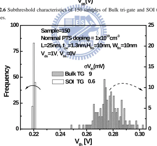
punch-through-stopper (PTS)……….15 Fig. 2.6 Subthreshold characteristics of 150 samples of Bulk tri-gate and SOI tri-gate
devices………..16 Fig. 2.7 Comparison of the Vth spread for Bulk tri-gate and SOI tri-gate devices. Vth is
determined by the constant current I0=(Wtotal/L)*100nA with Wtotal=2*Hfin+Wfin………16 Fig. 2.8 Dependence of Vth and σVth on substrate bias for Bulk tri-gate and SOI
tri-gate devices………...17 Fig. 2.9 Comparison of the γ dispersion for Bulk tri-gate and SOI tri-gate deices under (a) high drain and (b) low drain bias. γ ≡|ΔVth|/|ΔVbs|………18 Fig. 2.10 Impact of the PTS doping level on γ under (a) high drain and (b) low drain
bias………...19 Fig. 2.11 the impact of the PTS depth on subthreshold swing (SS) and body
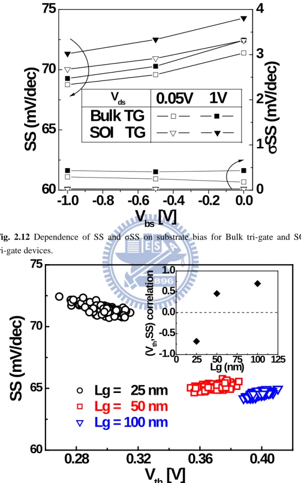
factor(γ )………..20 Fig. 2.12 Dependence of SS and σSS on substrate bias for Bulk tri-gate and SOI
tri-gate devices……….21 Fig. 2.13 Correlation plot between Vth and SS for Bulk tri-gate devices. The inset
shows the correlation coefficient for Bulk tri-gate devices with various channel lengths……….21 Fig. 3.1 Schematic tri-gate device structure and the coordinate definition of our
potential model……….34 Fig. 3.2 Potential distribution of the undoped tri-gate device at
(a)Y=L/2,Z=Wfin/2 ,(b)X=Hfin/2,Z=Wfin/2………35 Fig. 3.2 (c) Potential distribution of the undoped tri-gate device at Y=L/2,X=Hfin/2..36 Fig. 3.3 Subthreshold characteristics of undoped tri-gate devices with various channel
VII
lengths………..37 Fig. 3.4 Potential distribution along the fin height direction for tri-gate devices with
various BOX thicknesses………38 Fig. 3.5 (a)Potential distribution along the fin height direction for tri-gate devices with
various fin thicknesses and (b)Subthreshold Ids-Vgs characteristics for tri-gate devices with various fin thicknesses………...39 Fig. 3.6 (a) Potential distribution along the fin height direction for tri-gate devices
with an ultra thin BOX (5nm) under various substrate bias conditions, and (b) Subthreshold Ids-Vgs characteristics for tri-gate devices under various substrate bias conditions………40 Fig. 3.7 (a)Potential distribution along the fin height direction for tri-gate devices with
moderate thickness BOX (30nm) ,and (b) Subthreshold Ids-Vgs characteristics for tri-gate devices under various substrate bias conditions……….41 Fig. 4.1 Calculated contour of SS on a Wfin-Hfin plane under (a)low drain bias and
(b)high drain bias. The dashed lines indicate the SS contour map of the doped devices while the solid lines indicate that of the undoped device…47 Fig. 4.2 Body factor (γ ) dependence on fin aspect ratio (AR) under the (a) low drain
bias and (b) high drain bias. It is noted that γ is derived by threshold voltage at Vbs=0V and Vbs=-1V………..…48 Fig. 4.3 Calculated subthreshold carrier distribution on the cross section at the middle
of the channel for (a) device A , (b)device B, (c) device C and (d)device D. The origin of the axis “Hfin“ starts from BOX/channel interface. In addition, the origin of axis “Wfin“ starts from gate oxide/channel interface. It is noted that the carrier profiles are all extracted at Vgs=Vth-0.1V and Vbs=0V…...49 Fig. 4.4 Calculated contour of SS on a Wfin-Hfin plane for the tri-gate devices with
various channel lengths………50 Fig. 4.5 Body factor dependence on fin aspect ratio for the tri-gate devices with
L=20nm in the left figure and L=40nm in the right figure. It is noted that body factor is derived by threshold voltage at Vbs=1V and Vbs=-1V……..50 Fig. 4.6 (Left) Calculated contour map of SS on a Wfin-Hfin plane for the devices with
various EOT. (Right) Body factor (γ ) dependence on fin aspect ratio (AR) for the devices with various EOT. It is noted that γ is derived by threshold voltage at Vbs=1V and Vbs=-1V………...51 Fig. 4.7 Contour map of SS =70mV/dec for devices with various channel doping. The
equi-SS contour for the undoped devices is indicated by the dashed curve. The buried oxide thickness (Tbox) is 10nm………52 Fig. 4.8 Threshold voltage (Vth) versus aspect ratio (AR) for tri-gate devices with
VIII
undoped case is indicated by the dashed line………...53 Fig. 4.9 Threshold voltage (Vth) versus channel doping (Nch) for devices with AR=0.5 and AR=3. The buried oxide thickness (Tbox) is 10nm. The threshold voltage modulation ( ∆Vth ) by channel doping (from 1x1015cm-3 to 5x1018cm-3) is around 0.055V and 0.086V in tri-gate devices with AR of 0.5 and 3, respectively……….54 Fig. 4.10 Contour map of SS=70mV/dec for devices with various channel doping. The
equi-SS contour for the undoped devices is indicated by the dashed curve. The buried oxide thickness (Tbox) is 30nm………..55 Fig. 4.11 Threshold voltage (Vth) versus aspect ratio (AR) for devices with various
channel doping. The buried oxide thickness (Tbox) is 30nm. The undoped case is indicated by the dashed line……….56 Fig. 4.12 Threshold voltage (Vth) versus channel doping (Nch) for tri-gate devices with
AR=0.5 and AR=3. The buried oxide thickness (Tbox) is 30nm. The threshold voltage modulation (∆Vth) by channel doping (from 1x1015cm-3 to 5x1018cm-3) is around 0.083V and 0.106V in tri-gate devices with AR of 0.5 and 3, respectively………...57
IX
Table Captions
1
Chapter 1
Introduction
Because multiple gates can provide superior electrostatic control, tri-gate MOSFETs [1]-[4] have better immunity to short-channel effects (SCE), and can be used to extend the Moore’s Law in transistor scaling. In addition, random variation such as random dopant fluctuation [5]-[9], line edge roughness [10]-[11] has become a curial problem for nanoscale CMOS. Undoped or lightly-doped tri-gate MOSFETs can mitigate the channel random-dopant-fluctuation (RDF) problem for planer bulk MOSFETs [12].
In addition to random variability, subthreshold leakage current is another crucial problem for transistor scaling. To effectively control subthreshold leakage current, multi-threshold voltage technique [13]-[14] has been proposed to reduce power dissipation and maintain high performance. This low-power design technique uses high-Vth devices to suppress leakage currents and low-Vth devices to achieve high performance. In other words, multi-Vth is also important for tri-gate devices. Depending on the substrate, either SOI tri-gate or Bulk tri-gate can be used. To enable more efficient Vth modulation through substrate bias, SOI tri-gate can use ultra-thin buried oxide (BOX) [15]-[16] while Bulk tri-gate has to employ a punch-through-stopper (PTS) with high enough impurity concentration [17]-[20] right
2
beneath the lightly-doped channel. In this work, we use 3-D atomistic simulation to investigate the body-effect induced variability in Bulk tri-gate MOSFETs [21].
Due to the PTS-induced variability in Bulk tri-gate, SOI tri-gate with thin BOX seems to be a better device structure to enable threshold-voltage modulation. In order to physically assess the electrostatic integrity and facilitate device design for SOI tri-gate, we have derived a subthreshold model for SOI tri-gate considering the fringing field induced by the drain and source electrodes through the BOX. Although reference [22] has provided a subthreshold model for multi-gate SOI MOSFETs, the BOX-thickness scalability of the model is not accurate. In this work, we provide a more accurate subthreshold model for SOI tri-gate by improving the BOX-thickness scalability of the model in [22].
To enable power/performance optimization, the tri-gate SOI MOSFETs with thin BOX [15]-[16] has been recognized a promising device structure to achieve multiple threshold voltage (Vth). Whether different tri-gate device designs will impact the efficiency in Vth modulation is an important question. In this work, we investigate the multi-Vth device design of tri-gate SOI MOSFETs by using the derived analytical model. Based on the contour of equal subthreshold swing (SS), the impacts of device design on the threshold voltage modulation through substrate bias and channel doping are investigated.
3
This thesis is organized as follows. In chapter 2, we investigate the PTS-induced variability in Bulk tri-gate MOSFETs. In chapter 3, an analytical subthreshold model for SOI tri-gate devices with thin BOX is derived and verified with TCAD numerical simulation. In chapter 4, the impact of device design on multi-Vth modulation for SOI tri-gate is investigated by using the model derived in chapter 3. The conclusions are drawn in chapter 5.
4
Chapter 2
Body Effect Induced Variability in
Bulk Tri-gate MOSFETs
2.1 Introduction
Undoped/lightly-doped tri-gate MOSFET has been recognized as an important device structure to mitigate the channel random-dopant-fluctuation (RDF) problem for planer bulk MOSFET. Depending on the substrate, either SOI tri-gate or Bulk tri-gate can be used. Comparing with the SOI tri-gate, bulk tri-gate possesses lower wafer cost and higher process compatibility. References [17]-[18] have reported a successful 20 nm-FinFET fabrication on bulk silicon wafer. Both [17] and [18] employed the deep well implant to isolate the body from the substrate. This extra implantation process intended to suppress the leakage current beneath the channel region and was called as punch-through-stopper (PTS) layer. Several simulation works [18]-[20] have been made to investigate the device design optimization considering the PTS doping profile. However, these works have not considered the device variation introduced by the PTS. In addition, whether there is any difference regarding random variability between Bulk tri-gate and SOI tri-gate has rarely been known and merits investigation.
5
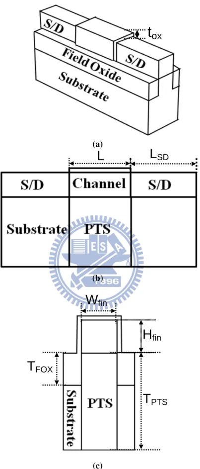
Although tri-gate MOSFETs have an improved immunity to short-channel effects (SCE), body effect in such device structure is usually weaker than planer MOSFETs [15]. To enable more efficient threshold-voltage (Vth) modulation and power/performance optimization through substrate bias, SOI tri-gate can use ultra-thin BOX [15]-[16] while Bulk tri-gate may employ the PTS with high enough doping concentration [20] right beneath the lightly-doped channel (Fig. 2.1). In this chapter, using 3-D atomistic simulation [23], we investigate the body-effect induced variability in Bulk tri-gate MOSFETs [21].
2.2 Device Design and Simulation Methodology
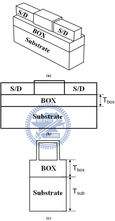
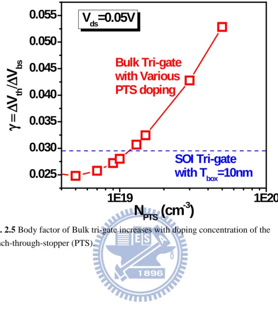
Bulk tri-gate and SOI tri-gate structures investigated in this chapter are based on the device design used in [24]-[25]. Schematics of Bulk tri-gate and SOI tri-gate structures are shown in Fig. 2.1 and Fig. 2.2, respectively. Channel length (Lg=25nm), channel doping (Nch=1x1017cm-3), gate oxide thickness (tox=1.3nm) and fin thickness (Hfin=Wfin=10nm) are designed identically for Bulk tri-gate and SOI tri-gate to ensure similar front gate controllability. As indicated in the Fig. 2.5, in order to achieve comparable body effect with SOI tri-gate, the PTS of Bulk tri-gate is designed with 1x1019 cm-3 in doping, 30 nm in depth (TPTS), 10 nm in width, and 25 nm in length, while the BOX of SOI tri-gate is designed with 10 nm in depth (Tbox), 20 nm in width and 65 nm in length (2*LSD+Lg). As indicated in the Fig. 2.1(b), the PTS doping
6
profile does not extend to the substrate below source/drain because the abrupt p-n junction between source/drain and PTS will induce significant band-to-band tunneling current. Other pertinent device parameters are listed in Table 2.1.
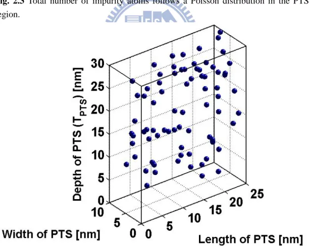
Discrete impurity atoms are randomly distributed in the PTS of Bulk tri-gate and the substrate of SOI tri-gate, respectively, in our 3-D atomistic simulation [23]. It is noted that the total number of impurity atoms in the PTS/substrate region follows the Poisson Random Distribution (Fig. 2.3) and the impurity atoms space distribution is shown in the Fig. 2.4. The detailed simulation procedure follows the methodology described in [38]. Since the continuous channel and source/drain doping profiles are identical for both the Bulk tri-gate and SOI tri-gate devices, the random variability assessed in this study stems from the PTS/substrate region. The value of gate work function used in our simulation is 4.5eV for both SOI tri-gate and bulk tri-gate.
2.3 Results and Discussion
2.3.1 Threshold Voltage Variability
Fig. 2.6 shows the dispersion of subthreshold characteristics for Bulk tri-gate and SOI tri-gate devices with 150 random samples. It is noted that the dispersion among the SOI tri-gate samples is negligible because the substrate doping variation is shielded by the thin BOX. Fig. 2.7 compares the spread of the threshold voltage for
7
Bulk tri-gate and SOI tri-gate devices. The nominal Vth of bulk tri-gate is larger than the SOI tri-gate because bulk tri-gate can deplete excess PTS ion charges in addition to the lightly doped channel. It can be seen that the Vth variation of Bulk tri-gate is significantly larger than that of SOI tri-gate. This is because the doping profile of PTS dramatically affects the total depletion charge (Qdep) enclosed by front gates and PTS. For example, near the interface of PTS and channel, one Bulk tri-gate sample with small number of discrete dopant atoms has larger Qdep than that of the other Bulk tri-gate sample with large number of discrete dopant atoms. For the SOI tri-gate, on the contrary, the heavily doped substrate beneath the BOX has negligible impact on Vth variation even an ultrathin (10 nm) BOX is used [39].
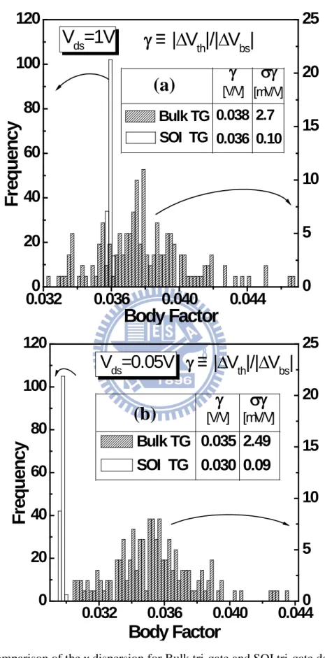
Fig. 2.8 shows the threshold voltage and its standard deviation (σVth) at different substrate biases (Vbs). The similarity of substrate sensitivity in two devices shows that the comparable body-effect has been design through tuning SOI thickness and PTS doping. It is also noted that the σVth dependence on Vbs is only about 1mV/V due to the heavily doped PTS. Fig. 2.9 (a) and (b) compare the spread of body-effect coefficient γ for Bulk tri-gate and SOI tri-gate devices under high and low drain bias, respectively. Bulk tri-gate shows slightly larger γ than that of SOI tri-gate because of the high enough PTS doping. The body-effect coefficient can be determined by [15] and [26]:
8
(
1)
2 1 2 3 si L SOI si L box ox C C C C C C + ϒ = × + + (2.1) ' ' 2 3 si L BULK ox C C C + ϒ = (2.2)However, to model the depletion layer formed in the substrate (Wdep sub_ ), the buried oxide capacitance (Cbox) in (2.1) should be replaced by
_ _
ox box si dep sub box
ox box si dep sub
t W C t W ε ε ε ε × = + (2.3)
In addition, the channel depletion capacitance ( '
si
C ) in (2.2) should consider the depletion region in PTS (Wdep ch_ ) as
' _ si si fin dep ch C H W ε = + (2.4)
Other capacitances are defined as
si si fin C =ε H (2.5) ox ox ox C =ε t (2.6) ( / ) ln( / ) L si fin C = C π × W r (2.7) ' ' ( / ) ln( / ) L si fin C = C π × W r (2.8)
It can be seen from (2.2) that the RDF in PTS will result in significant variation in the numerator of ϒBULK because Qdep ch_ as well as Wdep ch_ shows strong dependence on the PTS profile. For SOI tri-gate, on the contrary, the impact of the variation in Wdep sub_ is suppressed by the smaller and dominant buried oxide capacitance (Cburied =εox tbox).
9
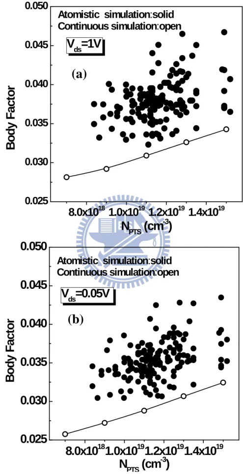
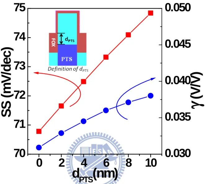
Fig. 2.10 (a) and (b) show the impact of the PTS doping level on the γ of Bulk tri-gate devices under high and low drain bias, respectively. It is noted that the nominal γ shows a discrepancy between continuous and atomistic simulations. It has been reported in [27] that PTS profile locating slightly away from the channel can enhance γ effectively because the carrier conduction path moves downward and the capacitance between the current path and substrate increases. This mechanism is also observed in our simulation result as indicated in the Fig. 2.11. Note that the horizontal axis dPTS is defined as the position of the PTS. It is plausible that this mechanism manifests itself through the position fluctuation of discrete dopant atoms near the interface of PTS and channel.
2.3.2 Subthreshold Swing Variability
Fig. 2.12 shows the substrate-bias dependence of subthreshold swing (SS) and its standard derivation (σSS) for Bulk tri-gate and SOI tri-gate devices. The similarity in subthreshold swing and its back-gate bias dependence in the two devices show that the device electrostatic integrity is similar by employing proper PTS doping/BOX thickness design. It is noted that the subthreshold swing variation is negligible because the channel is well controlled by the gate. Despite of the minor variation in SS, its correlation with Vth variation is also important for the circuit design considering mismatch [40]. Fig. 2.13 shows the correlation of threshold voltage and
10
subthreshold swing for Bulk tri-gate devices with a varying PTS doping. It can be seen from the inset that the correlation coefficient decreases with decreasing channel length. That means the subthreshold current mismatch characteristics may be different between the long and short channel devices. When the fin width and fin height are much smaller than the channel length, threshold voltage and subthreshold swing increase with the PTS doping concentration due to the enhancement of body effect. However, for the short channel devices, serious drain to source electric field coupling makes threshold voltage decrease and subthreshold swing increase. In other words, SCEs counterbalance the impact of PTS doping concentration on threshold voltage and subthreshold swing.
2.4 Summary
In this chapter, we investigate and report the body-effect induced variability in Bulk tri-gate MOSFETs. Through 3-D atomistic simulation, the random dopant fluctuations in the Punch-Through-Stopper (PTS) region of Bulk tri-gate devices are examined. Our study indicates that to achieve an efficient threshold-voltage modulation through substrate bias, the high-doping PTS region may introduce excess variation in Bulk tri-gate devices. This effect has to be considered when one-to-one comparisons between Bulk tri-gate and SOI tri-gate regarding device variability are made.
11 (a)
(b)
(c)
Fig. 2.1 Schematics of (a) 3-D Bulk tri-gate structure and the corresponding
cross-sectional view along (b) the channel and (c) the fin-width direction. It is noted that the PTS doping profile does not extend to the substrate below source/drain.
L
H
finW
finT
FOXL
SDt
oxT
PTS12 (a)
(b)
(c)
Fig. 2.2 Schematics of (a) 3-D SOI tri-gate structure and the corresponding
cross-sectional view along (b) the channel and (c) the fin-width direction.
T
subT
box13
Table 2.1 Device parameters of the simulated Bulk and SOI devices.
Bulk tri-gate SOI tri-gate
L 25nm 25nm LSD 20nm 20nm Wfin 10nm 10nm Hfin 10nm 10nm tox 1.3nm 1.3nm TPTS=30nm Tbox=10nm TFOX=10nm Tsub=20nm Channel Doping 1x1017cm-3 1x1017cm-3 Substrate doping 1x1017cm-3 1x1019cm-3 Source/Drain doping 2x1020cm-3 2x1020cm-3 Variation source PTS doping NPTS=1x1019cm-3 Substrate doping Nsub=1x1019cm-3
14
Fig. 2.3 Total number of impurity atoms follows a Poisson distribution in the PTS
region.
Fig. 2.4 Impurity atoms space distribution in the PTS region.
50 60 70 80 90 100 110 120
0
10
20
30
40
50
60
Fr
e
que
nc
y
Boron Number in PTS
Sample=150
15
1E19
1E20
0.025
0.030
0.035
0.040
0.045
0.050
0.055
Bulk Tri-gate
with Various
PTS doping
γ
=
∆V
th/∆
V
b sN
PTS(cm
-3)
SOI Tri-gate
with T
box=10nm
V
ds=0.05V
Fig. 2.5 Body factor of Bulk tri-gate increases with doping concentration of the
16 0.0 0.1 0.2 0.3 0.4 0.5 1E-11 1E-10 1E-9 1E-8 1E-7 1E-6 1E-5 1E-4 SOI tri-gate
I
ds(
A)
V
gs(V)
Bulk tri-gate Vds=0.05V Vbs=0V150 samples for Bulk tri-gate and SOI tri-gate
Fig. 2.6 Subthreshold characteristics of 150 samples of Bulk tri-gate and SOI tri-gate
devices. 0 5 10 15 20 25 0.22 0.24 0.26 0.28 0.30 0 25 50 75 100 σVth(mV) 0.6 9
F
req
u
en
cy
V
th[V]
SOI TG Sample=150 Nominal PTS doping = 1x1019cm-3 L=25nm, tox=1.3nm,Hfin=10nm, Wfin=10nm Vds=1V, Vbs=0V Bulk TGFig. 2.7 Comparison of the Vth spread for Bulk tri-gate and SOI tri-gate devices. Vth is determined by the constant current I0=(Wtotal/L)*100nA with Wtotal=2*Hfin+Wfin.
17
-1.0
-0.8
-0.6
-0.4
-0.2
0.0
0.0
0.1
0.2
0.3
0.00
0.01
0.02
0.03
V
ds=1V
V
ds=0.05V
V
th[
V]
V
bs[V]
Bulk TG
SOI TG
σ
V
th[
V]
Fig. 2.8 Dependence of Vth and σVth on substrate bias for Bulk tri-gate and SOI tri-gate devices.
18
0
5
10
15
20
25
0.032
0
0.036
0.040
0.044
20
40
60
80
100
120
[V/V] [mV/V]σγ
γ
0.036 0.10
0.038 2.7
Fr
e
que
nc
y
Body Factor
SOI TG
V
ds=1V
γ
≡ |∆V
th|/|∆V
bs|
Bulk TG
0
5
10
15
20
25
0.032
0.036
0.040
0.044
0
20
40
60
80
100
120
V
ds=0.05V
[V/V] [mV/V]γ
σγ
0.030 0.09
0.035 2.49
Fr
e
que
nc
y
Body Factor
SOI TG
γ
≡ |∆V
th|/|∆V
bs|
Bulk TG
Fig. 2.9 Comparison of the γ dispersion for Bulk tri-gate and SOI tri-gate deices under
(a) high drain and (b) low drain bias. γ ≡|ΔVth|/|ΔVbs|.
(a)
19
8.0x10
181.0x10
191.2x10
191.4x10
190.025
0.030
0.035
0.040
0.045
0.050
B
ody
Fa
c
tor
Atomistic simulation:solid
Continuous simulation:open
N
PTS(cm
-3)
V
ds=1V
8.0x10
181.0x10
191.2x10
191.4x10
190.025
0.030
0.035
0.040
0.045
0.050
V
ds=0.05V
Atomistic simulation:solid
Continuous simulation:open
B
ody
Fa
c
tor
N
PTS(cm
-3)
Fig. 2.10 Impact of the PTS doping level on γ under (a) high drain and (b) low drain
bias.
(a)
20
0
2
4
6
8
10
70
71
72
73
74
75
0.030
0.035
0.040
0.045
0.050
S
S
(
m
V
/d
e
c
)
d
PTS
(nm)
γ
(V
/V
)
Fig. 2.11The impact of the PTS depth on subthreshold swing (SS) and body factor
21
-1.0
-0.8
-0.6
-0.4
-0.2
0.0
60
65
70
75
0
1
2
3
4
S
S
(
m
V
/d
e
c
)
V
bs[V]
V
dsBulk TG
SOI TG
0.05V
1V
σ
S
S
(
m
V
/d
e
c
)
Fig. 2.12 Dependence of SS and σSS on substrate bias for Bulk tri-gate and SOI
tri-gate devices.
0.28
0.32
0.36
0.40
60
65
70
75
S
S
(
m
V
/d
e
c
)
V
th[V]
Lg = 25 nm
Lg = 50 nm
Lg = 100 nm
0 25 50 75 100 125-1.0
-0.5
0.0
0.5
1.0
(V
th,S
S
) cor
rel
at
ion
Lg (nm)
Fig. 2.13 Correlation plot between Vth and SS for Bulk tri-gate devices. The inset shows the correlation coefficient for Bulk tri-gate devices with various channel lengths.
22
Chapter 3
Analytical Subthreshold Model
For Tri-Gate SOI MOSFETs
With Thin Buried Oxide
3.1 Introduction
Due to superior electrostatic control, tri-gate MOSFETs provide improved immunity to short-channel effects (SCE) and become a promising candidate to extend the CMOS scaling. In order to physically assess the electrostatic integrity and facilitate device design for tri-gate SOI MOSFETs, an analytical subthreshold model is important. Although [22] has provided a subthreshold model for multi-gate SOI MOSFETs, the BOX-thickness scalability of this model is not accurate. In this work, we provide an analytical subthreshold model for tri-gate SOI MOSFETs by improving the BOX-thickness scalability of the model in [22].
Due to the homogeneous dielectric approximation in the BOX region, the original model in [22] is only suitable for the SOI tri-gate with BOX thickness from 10 to 30nm. When the BOX is thinner than 10nm, the discontinuity of the vertical electric field at BOX/channel interface becomes significant. We have considered this effect in our new model by making our potential solutions satisfy the boundary
23
condition (3.5). On the other hand, as the BOX thickness is larger than 30nm, the fringing field induced by the drain and source through the BOX leads to an increase in the channel potential. Since our potential solutions satisfy the boundary conditions (3.4b)-(3.4e) and (3.6) in the BOX region, the channel potential shift induced by the fringing field is well predicted by our model.
3.2 Subthreshold Model for Tri-gate SOI MOSFETs
with Thin BOX
3.2.1 Poisson’s Equation and Boundary Conditions
The schematic device structure of tri-gate SOI MOSFETs is shown in Fig. 2.1. The potential distribution in the subthreshold regime can be calculated by solving the 3D Poisson equation (3.1) within the silicon channel
2 2 2 ch ch ch ch 2 2 2 ch ( , , ) ( , , ) ( , φφφqN x , y ε z ) x y z x y z x y z ∂ +∂ +∂ = − ∂ ∂ ∂ (3.1)
Where and are the dielectric constant and doping concentration of the silicon fin, respectively.
In addition, the electrostatic potential in the buried oxide region can be described by 3D Laplace’s equation (3.2).
2 2 2
box box box
2 2 2 φφ ( , , ) ( , , φ 0 x y ) ( , ) z , x y z x y z x y z ∂ +∂ +∂ = ∂ ∂ ∂ (3.2)
24 described as ch ch ch gb fb ib 0 ox ε ( , , ) ( , , 0) φ φt εz z x y z V x y V = ∂ = − − ∂ (3.3a) ch ch ch gf fb if ox εφ ( , , ) ( , , φt εz ) fin fin z W x y z x yW V V = ∂ = − − ∂ (3.3b) ch ch ch gt fb it ox εφ ( φ ( , t , , ) x , ) ε fin fin x H x y z H y z V V = ∂ = − − ∂ (3.3c) ch( , 0, ) ms s φφ x z = − + V (3.3d) ch( , , ) ms d φφ x L z = − + V (3.3e) box( ox.u, , gu fb φ −t y z)=V −V (3.4a)
(
ms s)
gu fb(
)
box gu fb ox.u ox.u φ ( , 0, ) ( ) φ( ) x t t x z = V −V + − +V − V −V + (3.4b)(
ms d)
gu fb(
)
box gu fb ox.u ox.u φ ( , , ) ( ) φ( ) x t t V V V z V L V x = − + − + − − + (3.4c)(
gb fb)
gu fb(
)
box ib gu fb ox.u ox.u ( ) φt ( ( ) x t t , , ) V x y − = V −V + −V − V −V + (3.4d)(
gf fb)
gu fb(
)
box fin if gu fb ox.uox.u ( ) φW t ( ) x t t ( , ,x y + )= V −V + V −V − V −V + (3.4e) ch box ch ox 0 0 φφ εε ( x x , , ) ( , , ) x x x y z x y z = = ∂ ∂ ∂ = ⋅ ∂ ⋅ (3.5) ch box 0 0 φφ y y ( , , ) ( , , ) x x x y z x y z = = ∂ =∂ ∂ ∂ (3.6)
Here ε and ch ε are the permittivity of channel material and oxide, respectively. ox
fin
W ,Hfin and L are defined as fin width, fin height, and channel length, respectively.t ,ib tif
25
dielectric, top gate dielectric , and buried oxide, respectively.Vgb, Vgf, Vgt, Vgu, V , s and V are the voltage biases of back gate, front gate, top gate, buried gate, source, d and drain terminal, respectively. V is the flat-band voltage for these gate fb terminals.φ is the built-in potential of the source/drain to the channel. ms
3.2.2 Power Series Solution to Boundary Value Problems
To solve the potential solution in (3.1) using the above boundary conditions, we divide the 3D boundary value problems into three sub-problems, including 1-D Poisson equation, 2-D, and 3-D Laplace equation [22]. Using the superposition principle, the 3D Poisson equation can be solved sequentially by 1-D Poisson equation, 2-D and 3-D Laplace’s equation. So the complete channel potential solution is φφch( , , )x y z =φφch,1( )x + ch,2( , )x y + ch,3( ,x y z, ) , where φ ( )ch,1 x , φch,2(x y, ) and
ch,3( ,
φ x y z, ) are the solutions of 1-D, 2-D, and 3-D sub-problems in the channel,
respectively. The 1-D solution can be expressed as
2 ch ch,1 ch qN φx Ax B 2ε ( )x = − + + (3.7) 2 ch ch gt fb gu fb fin fin it ch ox ch ch fin it ox.u ox ox qNε ( ) ( ) (H 2H t ) 2εε A εε H t t εε V −V − V −V + + = + + ⋅ (3.8) ch ox.u gu fb ox ε B A t ( ) ε V V = ⋅ + − (3.9)
In solving the 2-D and 3-D sub-problems, the boundary conditions [(3.3a)-(3.3c)] of gate oxide/channel interface are simplified by converting the gate oxide dielectric
26
thickness to (εεch / ox) times and replacing the gate oxide region with an equivalent channel-material region. The electric field discontinuity across the gate oxide and channel interface can thus be eliminated. In other words, the channel region and the gate oxide region are treated as homogeneous cuboids with an effective width
eff
W and an effective Heff defined by (3.10) and (3.11), respectively.
ch eff fin if ib ox ε W W (t t ε ) = + + (3.10) ch eff fin it ox ε H H t ε = + (3.11)
The 2-D solution φch,2(x y, ) can be calculated using the method of separation of variables
(
)
(
)
ch,2 n n
n 1 eff eff eff
nπnπnπ
φ, B sinh E sinh L y sin x
H H H x y y ∞ = = + − ⋅
∑
(3.12a) where( )
( )
( )
n ch eff n 3 ms d 2 ch ( 1) 1 1 qN 2 ( 1 2AH 1 1 ( 1) B φ) 2( επππ nπ nπL sinh ) n n n eff eff V B n n n H H ⋅ − − − = − + + − + − − − ⋅ − (3.12b)( )
( )
( )
n ch eff n 3 ms 2 ch ( 1) 1 1 qN 2 ( 1 2AH 1 1 ( 1) E φ) 2( επππ nπ nπL sinh ) n n eff e n ff s V B n H n n H ⋅ − − − = − + + − + − − − ⋅ − (3.12c)For the channel/buried oxide interface, both the potential distribution in the channel φch,3(x y z, , ) and that in the buried oxide φbox,3(x y z, , ) have to be
27
considered to satisfy the boundary conditions (3.5) and (3.6). Similarly, the 3-D solution φch,3(x y z, , ) can be obtained and expressed as
2 2 , 1 1 2 2 , c 1 h 3 1
, ( , , ) sinh sinh sin
sinh ( ) φ sinh n m n m eff eff n m eff n m eff eff n m n m x y z B z x y H L H L n m n E W z x H L H
π
π
π
π
π
π
π
∞ ∞ = = ∞ ∞ = = = + ⋅ ⋅ ⋅ + + ⋅ − ⋅ ∑∑
∑∑
1 2 2 , 1 sinsinh ( eff ) sin sin
eff e i m i m ff m y L i m i m H x z y W L W L H
π
π
π
π
π
∞ ∞ = = ⋅ + − ⋅ ⋅ +∑∑
(3.13a)The coefficientsBn m, ,En m, and Hi m, in (3.13a) can be expressed as
(
)
( )
( )
( )
n eff ch , 2 2 3 ch n 2 1 sinh 1 ( 1) 2( ) 2 1 ( 1) ( 1) 1 ( 1) 1 ( 1) sinh / 2AH 1 π 2 qN επ nπ 1 B 2 n m eff eff n gf fb m n n eff m eff eff B n m W H L V V B n H m n n L n L m H L n H π π π π π π − + ⋅ − = × + ⋅ − − − − + − − × − − ⋅ − − − − ⋅ + × 2 2 1 sinh / 2 1 eff n eff n L m L H E L L n L m H m π π − ⋅ + × (3.13b)28
(
)
( )
( )
( )
n eff ch , 2 2 3 ch n 2 1 sinh 1 ( 1) 2( ) 2 1 ( 1) ( 1) 1 ( 1) 1 ( 1) sinh / 2AH 1 π 2 qN επ nπ 1 B 2 n m eff eff n gb fb m n n eff m eff eff E n m W H L V V B n H m n n L n L m H L n H π π π π π π − + ⋅ − = × + ⋅ − − − − + − − × − − ⋅ − − − − ⋅ + × 2 2 1 sinh / 2 1 eff n eff n L m L H E L L n L m H m π π − ⋅ + × (3.13c)(
)
(
, ,)
, , , , sinh sinh i m ox u n m i m i m i m eff t RHS H LHS H λ λ ⋅ = × ⋅ (3.13d) where 2 2 , i m eff i m W L π π λ = + ,(3.13e)(
)
(
,)
ch ox , , , , , , , , sinh cosh( ) cosh( ) s ε ε inh i m ox u i m i m i m ox u i m i m eff i m eff t LHS t H H λ λ λ λ λ λ ⋅ = + ⋅ , (3.13f)29
(
)
ch n 1 ox ch n,m , 2 2 ox 1 1 ( 1) sinh sinh 2 1 ( 1) / / 2 2 1 1 1 ( 1) s ε B ε ε 2 / B h ε in m i eff eff n m n eff eff eff i eff eff n n L n L m L H m L H n RHS E L n L L n L H i H m H m i W W π π π π π π γ π ∞ = − − − − = ⋅ + ⋅ × + × + × − − + ⋅ ⋅ × ∑
(
)
(
)
n,m 1 , , 2 2 , , , , 2 n E K 1 sinh / 2 1 1 / / 1 1 ( 1) sinh sinh / / 2 2 1 n m eff n m eff eff eff eff n m n m eff n eff m ox u ox u n ox W W i W n W H i W i W n L n L m L t m L t P L n L L t m γ π π γ γ π π π π π π ∞ = × ⋅ ⋅ + ⋅ ⋅ + + − − − ⋅ + ⋅ × +∑
(
)
(
)
(
)
2 1 , , , n,m n,m , 2 2 , , 2 1 ( 1) ( 1) 1 1 1 ( 1) sinh sinh / / 2 2 1 1 / / i n n ox u ox u i n m eff n m eff eff eff eff eff n m n m eff eff n t i n L t m W W i W i W K P W W i W i W π π π π π π ∞ = ⋅ − − − × + × − − Γ ⋅ Γ ⋅ − ⋅ ⋅ + ⋅ ⋅ Γ Γ + + × ∑
1 , ( 1)n ox u n n t π ∞ = ⋅ − × ∑
, (3.13g) 2 2 , , n m ox u n m t L π π Γ = + ,(3.13h) and 2 2 , n m eff n m H L π π γ = + .(3.13i)The coefficientsK , n P , n Kn,mandPn,m in (3.13g) stem from the 2-D and 3-D
potential solution in the buried oxide region, and they can be expressed as
(
)
1 n ms s , ( 1) φ π nπL si 2 nh ox u n K n B t V + − = − + − (3.13j)(
)
1 , n ms ( 1) φ π nπL sinh 2 d ox u n P n B t V + − = − + − (3.13k)30
(
)
1 , 2 2 , , 2 2 , , n , 2 ( 1) 1 ( 1) ( ) 1 1 1 ( 1) sinh sinh / / 2 2 sinh 1 1 n m gf fb m n m ox u ox u n eff ox u ox u ox u V V B m n n L n L K m L t m L t n m K P W L L n L n L t L t m t m π π π π π π π π + − − − × − − − − = − ⋅ − ⋅ + ⋅ + × + × (3.13m)(
)
1 , 2 2 , , 2 2 , , n , 2 ( 1) 1 ( 1) ( ) 1 1 1 ( 1) sinh sinh / / 2 2 sinh 1 1 n m gb fb m n m ox u ox u n eff ox u ox u ox u V V B m n n L n L P m L t m L t n m K P W L L n L n L t L t m t m π π π π π π π π + − − × − − − − − = − ⋅ − ⋅ + ⋅ + × + × (3.13n)Finally, analytical expressions for the potential in the channel and BOX region are shown as equation (3.14) and (3.15), respectively.
ch( , , ) ch,1( ) ch,2( , ) ch,3( , φφ x y z =φφ x + x y + x y z, )
(
)
(
)
(
)
, 2 ch n n n 1 ch eff , , , 1 eff eff , 1 1 sinh sinh ( ) sinh s qN nπnπnπx Ax B B sinh E sinh L y sin x
2εH H H sinh in n m n m n m n m eff n m ef i m m f B z E W z n m H y L y x H ∞ γ γ π π ∞ ∞ = = = = = ⋅ + ⋅ − × ⋅ − + + + + − ⋅ + +
∑
∑
∑
(
)
1 , ( ) sin sin i m eff e i ff i m H x z y W L π π λ ∞ ∞ = − ⋅ ⋅ ∑∑
(3.14)box,1 box,2 box,3
( , , ) ( ) (
31
(
)
(
)
(
)
ox,u ch , g , , , , 1 1 , u fb n n n 1ox ox,u ox,u ox,u
nπ(x+t )
ε nπnπ
( ) ( ) K sinh P sinh L y sin
εt t t sinh sinh ( ) ( ) sinh n m n m n m n m eff n m ox x u o u x t V V A K z P W z n x t t y ∞ π = ∞ ∞ = = = + + − + + − ⋅ Γ ⋅ + Γ ⋅ − × + +
∑∑
∑
(
)
, , , , , , 1 1 , sinh( ) sinh sinh( )sin i m i m ( ox u) sin sin
ox u i m eff eff i m i m ox u m i m y H H t x t z y L W L λ π λ π π λ ∞ ∞ = = ⋅ ⋅ ⋅ + ⋅ ⋅ ⋅ +
∑∑
(3.15)Based on the potential solution, the subthreshold current can be calculated by [22] min 2 ( / ) ( , , )/ 0 0 1 1 fin fin DS ch H W qV kT q x y z kT i DS ch n kT I q e e dzdx N q L φ µ − = − ⋅ ⋅
∫ ∫
(3.16)where φch( ,x ymin, )z is the minimum potential along the channel direction.
3.3 Model Verification
We verify our potential solution with the TCAD Silvaco ATLAS [28]. The schematic device structure is indicated in Fig. 3.1. In order to demonstrate the improvement of our model, we also compare our model with the model in [22] (dashed lines) which adopted a simpler boundary condition at the channel/BOX interface. Fig. 3.2 (a), (b), and (c) show the potential distribution in an undoped tri-gate SOI MOSFET. The discrepancy between the dashed lines and TCAD is significant because the homogeneous dielectric approximation in the BOX region does not consider the fringing field induced by the drain and source through the BOX. This longitudinal coupling causes an increase in channel potential near the substrate.
32
In other words, the channel potential shift induced by drain bias is similar to a positive substrate bias. It results in threshold voltage lowering and subthreshold swing degradation. As indicated in Fig. 3.3, as channel length scaled down below 20nm, the model without considering drain to source coupling fails to match the TCAD result even for a low drain bias condition.
Fig. 3.4 shows the potential distribution along the fin height direction for tri-gate devices with various BOX thicknesses. It is noted that our model shows good agreement with the TCAD simulation while the model in [22] (dashed line) fails to predict the potential profiles for the thin-BOX cases. Fig. 3.5 (a) shows the potential distribution along the fin height direction for long channel devices with various fin thicknesses. It is noted that the discrepancy of the model in [22] with TCAD increases with decreasing fin thickness. The potential barrier rise at the BOX/channel interface leads to a negligible impact on subthreshold current for devices with larger fin width. However, the same potential barrier perturbation introduces significant errors in the small dimension device. As indicated in Fig. 3.5 (b), it is difficult for the dashed lines to agree with TCAD results even for the devices with good electrostatic integrity.
Fig. 3.6 (a) and (b) show the potential distribution along the fin height direction and the subthreshold current characteristics, respectively. It can be seen that the model in [22] fails to capture the impact of substrate bias on subthreshold characteristics,
33
while our new model shows satisfactory accuracy. The error of the model in [22] increases with the thickness of the BOX. Fig. 3.7 (a) and (b) show the potential and subthreshold characteristics for SOI tri-gate with a 30-nm thick BOX. Apparently, the potential distribution along the fin height direction for the model in [22] cannot faithfully respond to the substrate bias, and the subthreshold current shows wrong substrate-bias sensitivity.
3.4 Summary
We have derived a subthreshold model for tri-gate SOI MOSFETs considering the fringing field induced by the drain and the source through the BOX. Our model is better than the model in [22] because the potential solution in the BOX region is exactly solved. Based on the BOX potential, the boundary conditions of the channel region are improved. With this improvement, our model has successfully predicted the SCEs and the substrate sensitivity for tri-gate SOI devices with various BOX thicknesses. This model enhancement is especially important for the multi-Vth scheme. Based on our new model, the device design of multiple-threshold voltage in tri-gate SOI devices will be investigated in the next chapter.
34
fin body
Insulator
t
itt
ifz=t
ifZ
X
Y
(0,0,0)
W
finL
t
ox,ut
ibH
finBOX
Fig. 3.1 Schematic tri-gate device structure and the coordinate definition of our
35
-6
-4
-2
0
2
4
6
8
10
12
-1.6
-1.2
-0.8
-0.4
0.0
0.4
V
bs=-1V
V
bs=0V
V
bs=1V
Channel region
P
o
ten
ti
al
[V
]
Fin Height Direction, X [nm]
BOX
Undoped
L=20nm,EOT=0.8nm
W
fin=H
fin=10nm,T
box=5nm
V
ds=1V,V
gs=0V
Symbol:TCAD
Dashed Lines:Original Model [10]
Solid Lines:New Model
(a)
0
2
4
6
8
10
12
14
16
18
20
0.2
0.4
0.6
0.8
1.0
V
bs=0V
V
bs=1V
V
bs=-1V
P
o
ten
ti
al
[V
]
Channel Direction, Y [nm]
Undoped
L=20nm,EOT=0.8nm
W
fin=H
fin=10nm,T
box=5nm
V
ds=1V,V
gs=0V
Symbol:TCAD
Solid Lines:Original Model [10]
Dashed Lines:New Model
(b)
Fig. 3.2 Potential distribution of the undoped tri-gate device at (a)Y=L/2,Z=Wfin/2 ,(b)X=Hfin/2,Z=Wfin/2.
Original Model [22]
36
0
2
4
6
8
10
0.2
0.3
0.4
0.5
V
bs=0V
V
bs=1V
V
bs=-1V
P
o
ten
ti
al
[V
]
Fin Width Direction , Z [nm]
Undoped L=20nm,EOT=0.8nm
W
fin=H
fin=10nm,T
box=5nm ,V
ds=1V,V
gs=0V
Dased Lines:Original Model [10]
Solid Lines:New Model
Symbol:TCAD
(c)
Fig. 3.2 (c) Potential distribution of the undoped tri-gate device at Y=L/2,X=Hfin/2.
Original Model [22]
37
-0.1
0.0
0.1
0.2
0.3
1E-12
1E-11
1E-10
1E-9
1E-8
1E-7
1E-6
1E-5
1E-4
1E-3
Symbol:TCAD
Dashed Lines:Original Model[10]
Solid Lines:New Model
Undoped
EOT=0.8nm,W
fin=H
fin=10nm,T
box=5nm
V
bs=0V,V
ds=1V
I
d
s
[
V]
V
gs
[V]
L= 100nm
L= 60nm
L= 40nm
L= 20nm
L=15nm
Fig. 3.3 Subthreshold characteristics of undoped tri-gate devices with various channel
lengths.