Abstract—In this paper, a semiself-protection scheme is pro-posed and developed for gigahertz output electrostatic-discharge (ESD) protection. The output transistor acts as a trigger device to trigger the ESD protection device, and then, it is turned off when the ESD protection device turns on. Thus, the capacitance of a gigahertz high-frequency output pad can be minimized because this scheme is without any additional trigger device or any passive component.
Index Terms—Electrostatic discharge (ESD), radio frequency, silicon-controlled rectifier (SCR).
I. INTRODUCTION
T
HE electrostatic-discharge (ESD) performance of a silicon-controlled rectifier (SCR) is much superior than that of a grounded-gate (GG) n-channel metal–oxide– semiconductor field-effect transistor (n-MOSFET) because of its high-current and low-voltage characteristics. Designed with a much smaller dimension, SCRs can obtain the same or better ESD performance compared with a GGNMOS. SCRs have become a good ESD protection device for radio-frequency or high-frequency (HF) circuit designs.Although an SCR has robust ESD performance, it cannot prevent an ESD from damaging protected devices appropri-ately due to its high trigger voltage Vt1 [1]. The protected
device could be damaged before the SCR turns on. Thus, many kinds of triggering devices are designed to reduce the Vt1 of
an SCR. The triggering devices include n-MOSFETs [1]–[4], p-n-p bipolar transistors [5], p-channel MOSFETs [6], and diode-string structures [7]. The triggering device often needs to be incorporated with a resistor (R1 in Fig. 1) to prevent the high ESD current from damaging integrated circuits (ICs). The resistor might be the well-shunt resistor (R1 in Fig. 1) of an SCR [1], a discrete resistor [2], or the silicide-blocking resistor of a triggering device [3], [4]. Apparently, a resistor will induce a voltage across the resistor when the current flows through the triggering device. This increases the device’s Vt1; thus, an
Manuscript received December 28, 2010; revised March 30, 2011 and April 8, 2011; accepted April 11, 2011. Date of publication May 23, 2011; date of current version June 22, 2011. The review of this paper was arranged by Editor M. J. Kumar.
J.-H. Lee is with the Richtek Technology Corporation, Hsinchu 30288, Taiwan, and also with the Realtek Semiconductor Corporation, Hsinchu 300, Taiwan (e-mail: [email protected]).
S.-C. Huang and K.-H. Chen are with the Institute of Electrical and Control Engineering, National Chiao Tung University, Hsinchu 300, Taiwan (e-mail: [email protected]; [email protected]).
H.-D. Su is with the Richtek Technology Corporation, Hsinchu 30288, Taiwan (e-mail: [email protected]).
Color versions of one or more of the figures in this paper are available online at http://ieeexplore.ieee.org.
Digital Object Identifier 10.1109/TED.2011.2143717
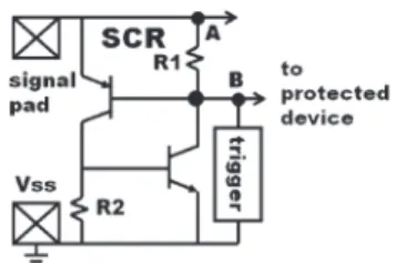
Fig. 1. SCR has the triggering device behind a resistor. The protected device needs to connect to node B and not to Node A.
SCR cannot prevent an ESD from damaging protected devices if the protected devices are in parallel with the SCR (node A in Fig. 1) [8]. Regardless of the input gate [1] or the output drain terminal [2], the protected devices had better connection to the node after the resistor (node B in Fig. 1) instead of the node before the resistor (node A in Fig. 1). However, a resistor can induce noise, reflection, a secondary harmonic, and power gain loss at HF applications. Thus, putting a transceiver and a receiver behind a resistor is not allowed for most HF designs.
It has been reported that the structures of a GGSCR [3] and a p-n-p triggering SCR [5]) allow a signal pad to connect to a protected device without passing through a resistor. How-ever, both structures cannot be used for driving circuits. It is because the triggering device of the GGSCR [3] has a ballast resistor on the drain terminal and a series resistor on the source terminal. Although the triggering devices of the modified p-n-p triggering SCRs [5], [6] are revised to MOSFETs, they are all located behind the SCR’s well-shunt resistors. Furthermore, diode-triggering SCR structures have been discussed in [9] and [10]. Silicon-on-insulator SCRs, 3-D technology computer-aided design, and an insulated-gate bipolar transistor plugged in an SCR are described in [11]–[13]. However, all the above SCR structures have the disadvantages of bad (or no) output driving capabilities.
If an n-MOSFET designed with the minimum design rules can be placed in parallel with an SCR, it can be used as the output transistor during IC normal operation. The simulation of designing an n-MOSFET in parallel with an SCR is reported in this paper. With the proper layout for the n-MOSFET and the SCR, the n-MOSFET can be turned only on at the initial transient time and can be turned off after the SCR is triggered on. Due to the short turn-on time, Joule heating (power× time) caused by an ESD is too small to damage the output transistor. Since the output transistor can be turned on at a short time and most ESDs are dissipated by the primary ESD protection device SCR, this protection scheme is called the semiself-protection (SSP) scheme.
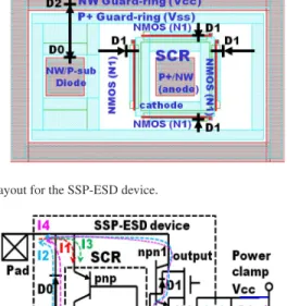
Fig. 2. Layout for the SSP-ESD device.
Fig. 3. Equivalent circuit and current paths for SSP-ESD devices under four different zapping modes.
The technology of this paper is a 0.18-μm 1.8/3.3-V silicide complementary MOS (CMOS) process. Although the architec-tures in this paper are verified by using 1.8-V devices with a gate-oxide thickness equal to 32 Å, it can also be modified as the 3.3-V operation. This paper is processed on a dual-well (p-well and n-well) process and a p-type wafer. Except for n-well regions, they are p-well regions.
II. DEVICESTRUCTURE ANDANALYSIS A. SSP ESD Device
Fig. 2 shows the layout of the SSP-ESD device. The SSP-ESD device includes the following:
1) an n-type well (NW) to the p-type substrate diode (D0); 2) an SCR and the output transistor (n-MOSFET) N1 and its
parasitic diode (D1); 3) p+ and NW guard rings;
4) The parasitic diode (D2) between the two guard rings. Diodes D0 and D1 are designed for negative ESD stress. The SCR with the output transistor N1 is designed for positive ESD stress. The NW and p+ guard ring are designed for ICs’ latch-up prevention and for PAD-VCCESD protection under positive
ESD stress.
Fig. 3 shows the equivalent circuit and the current paths of the SSP-ESD device with a power clamp (PCL) device under four kinds of ESD zapping modes. The four kinds of ESD zapping modes are: (+) PAD-VSS, which is the positive ESD
event at the signal pad with respect to VSS; (−) PAD-VSS,
which is the negative ESD event at the signal pad with respect to VSS; (+) PAD-VCC, which is the positive ESD event at the
signal pad with respect to VCC; and (−) PAD-VCC, which is
the negative ESD event at the signal pad with respect to VCC.
Although the SSP-ESD device is only designed for (+/−)
Fig. 4. Detailed layout for the SSP-ESD device in Fig. 3.
PAD-VSS protections, it can also provide (+/−) PAD-VCC
ESD protections as it cooperates with the PCL device. The discharge current paths of the SSP-ESD device with the PCL device under the four kinds of ESD zapping modes can be depicted as follows. For (+) PAD-VSS, current I1 flows from
the signal pad through the SCR of the SSP-ESD device to VSS.
For (−) PAD-VSS, current I2 flows from VSSthrough the diodes
D0 and D1 of the SSP-ESD device to the signal pad. For (+) PAD-VCC, current I3 flows from the signal pad through the SCR
of the SSP-ESD device and the combined paths of the diode D2 of the SSP-ESD device and the diode D3 of the PCL device to VCC. For (−) PAD-VCC, current I4 flows from VCCthrough
the parasitic bipolar n-p-n 3 of the PCL device and the diodes D0 and D1 of the SSP-ESD device to the signal pad. The SCR anode area size is 6 μm× 6 μm.
B. SCR
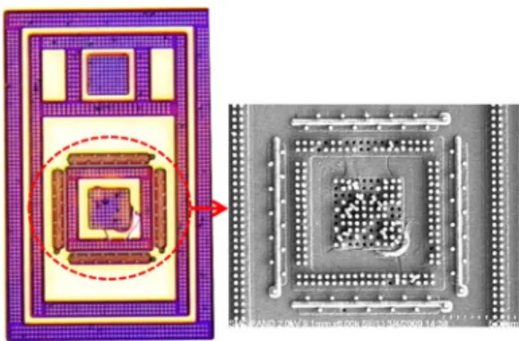
Fig. 4 shows the detailed layout for the SCR of the SSP-ESD device. Unlike the NW of the conventional SCR [1]–[13] with the n+ and p+ diffusions, the NW of this SCR only has the p+ diffusion. Without the n+ diffusion in the NW, the p-n-p bipolar transistor is an open base transistor (see Fig. 3). From the testing results, the SCR still can be turned on by an ESD without wasting layout areas for forming a base resistor. Thus, the SCR can be turned on by an ESD more easily and does not need to waste layout areas to form a base resistor. Without wasting the area, the SCR dimension can be minimized. Thus, it can get smaller capacitance compared with the conventional SCR. In addition, the shape of the SCR is designed as a square type for getting the smallest layout perimeter under an assigned layout area. This kind of design can also obtain a smaller sidewall capacitance value. The SCR’s cathode is designed as a ring and surrounds the SCR’s anode. The output transistor is composed of four 1.8-V n-MOSFETs, which are outside and surround the SCR’s cathode.
Except for the space between contacts, the output transistor is designed with the minimum layout rules to minimize its total capacitance. The finger width and the total channel width of the output transistor are equal to 10 and 40 μm, respectively. The source of the output transistor is located close to the cathode of the SCR than the drain of the output transistor. This kind of architecture can make the high ESD current not flow through the output transistor when the SCR turns on since the output transistor is outside the SCR (see Fig. 5). Unlike the conven-tional n-MOSFET trigger devices of the SCRs [2], [4], [8] with
in Fig. 4.
Fig. 6. Equivalent circuit for the MLVTSCR.
the silicide-blocking drain regions, the trigger device (output transistor) of the SSP-ESD device is a fully silicide device. Instead of the silicide-blocking drain regions, the contacts on the source and drain (S/D) regions of the output transistor are designed with the stagger S/D contact type and a large contact-to-contact space [14]. Without the silicide-blocking layer, the drain contact to the poly-gate space and the source contact to the poly-gate space can be designed with the minimum process rules. This scheme can get the smallest capacitance and series resistance for the n-MOSFET trigger device. With low capacitance and resistance, such a trigger device can be used as the output transistor for HF operation.
C. Simulated Current for the SCR
Fig. 6 shows the cross section and the equivalent circuit of the modified low-voltage-triggered SCR (MLVTSCR) [4]. The difference between an LVTSCR [1] and the MLVTSCR is that the drain region of the MLVTSCR does not overlap the NW and connects to the pad directly. The SSP ESD is a new version of the MLVTSCR. For this kind of an SCR, the source of the trigger device shares the same region with the cathode of the SCR. In addition, the drain region of the trigger-ing device is located between the SCR cathode and the SCR anode. Apparently, the triggering device is within the SCR. TSupprem 4 for the process simulation and the device forma-tion and MEDICI for the electrical simulaforma-tion are adopted in this paper.
From the simulation result in Fig. 7(a), the current flows from the drain region of the triggering device to the source region of the triggering device and the VSSp+ diffusion at the transient
before the trigger. This implies that the n-p-n bipolar transistor of the triggering device will be turned on first. Then, the current can also flow from the p+ diffusion in the NW to the VSSp+
diffusion except the n-p-n bipolar current [see Fig. 7(b)]. This implies that the p-n-p bipolar transistor has been triggered to the ON-state at this transient. As the stress current increases, the currents not only flow from the p+ diffusion of the NW but
Fig. 7. Simulated current flowing lines of the MLVTSCR transients. (a) Before the trigger. (b) At the trigger. (c) After the trigger.
also flow from the drain region of the triggering device to the source region of the triggering device and the VSSp+ diffusion
[see Fig. 7(c)].
Both the SCR and the triggering device are turned on to drive the MLVTSCR into a stable snapback region after the triggering transient because the cathode is closer to the drain region than the anode. If the electrons can flow from the SCR cathode to the SCR anode, they will be able to flow to the drain region of the triggering device. For such an SCR, the ESD current flows through the triggering device even when the SCR has turned on. For preventing output devices from ESD damage, the drain region of the triggering device is often designed with a ballast
Fig. 8. Simulated current flowing lines for the SSP-ESD device at the tran-sients after the trigger.
resistor. However, adding a ballast resistor is not allowed for the output transistor under the gigahertz application.
If the S/D terminals are exchanged, the triggering device will be located outside the SCR, as shown in Fig. 5. For the transients before and at the trigger, the ESD behaviors of this new architecture are the same as those of the MLVTSCR, but the S/D regions are exchanged. However, for the transient after the trigger, the ESD behavior of the new architecture is apparently different from that of the MLVTSCR, as shown in Fig. 8; it shows that the current can only flow through the SCR and not through the triggering device.
When the SCR is turned on, the triggering device could be turned off and kept far away from the ESD stress. It implies that most ESD charges are dissipated by the SCR, and only few ESD charges flow through the triggering device at the beginning of the ESD pulse. Due to the short turn-on time, there is no time to generate enough Joule heating for damaging the triggering device. Thus, the triggering device can be used as the output transistor without sacrificing its HF characteristics. Since the output transistor can protect itself before the SCR turns on and can be protected when the SCR turns on, this protection scheme is called the SSP scheme.
Furthermore, the big differences between Figs. 7(c) and 8 are that there are high current densities (as the current flow lines) in the Fig. 7(c) NMOS transistor, but there are none in Fig. 8.
III. EXPERIMENTALRESULT ANDDISCUSSION A. ESD Behavior of the SSP-ESD Device
In order to investigate the ESD behavior of the SSP-ESD device, a digital oscilloscope with a 500-MHz bandwidth and a 2 GSa/s sample rate is used to measure the voltage and current waveforms of the SSP-ESD device during a human-body-model (HBM) zapping event.
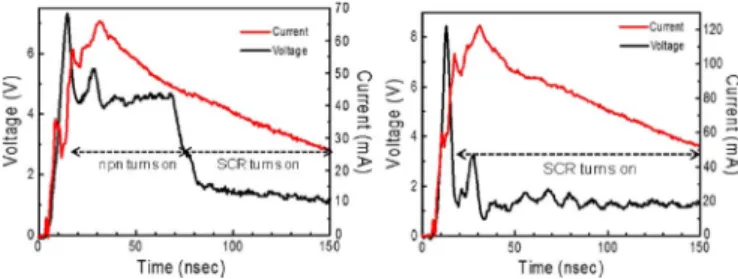
Fig. 9 shows the real-time I–t and V –t characteristics of the SSP-ESD device under the +100- and +200-V/VSSHBM
zap-ping events. For the HBM +100-V/VSSzapping event, the
cur-rent waveform sharply rises to its peak value (100 V/1.5 KΩ ∼= 66 mA), and then, it decays with a resistance–capacitance time constant (∼150 ns). About the voltage waveform, there are
Fig. 9. Real-time I–t and V –t characteristics of the SSP-ESD device under (left picture) the +100 V/VSS HBM zapping event and (right picture) the
+200 V/VSSHBM zapping event.
two snapback regions. The first snapback (the voltage is about 4.5 V) occurs at the time from 20 to 80 ns; it comes from the turning on of the n-p-n bipolar transistor. The second snapback (the voltage is about 1.5 V) occurs after 80 ns; it comes from the turning on of the SCR. The above verifies that the n-p-n bipolar transistor can be turned on to clamp the pad voltage first, and then, the SCR can be triggered on for the SSP-ESD device during the SSP-ESD zapping event. However, for the + 200 V/VSS HBM zapping event, there is only one snapback
voltage (1.5 V) from the turning on of the SCR. This implies that the SCR can be triggered to theON-state instantaneously if the zapping voltage is larger than +200 V.
Before the snapback, the voltage rapidly rises until the de-vice avalanche breakdown occurs at the drain junction of the triggering device in Fig. 9. Although the voltage can reach as high as 8 V, the transient of 8 V cannot damage the gate oxide because the gate-oxide transient endurance voltage is much larger than the gate-oxide direct-current (dc) endurance voltage in the 0.18-μm process [15]. This induces substrate-current generation. As the substrate substrate-current flows through the p-type substrate and raises the substrate voltage up to a value larger than 0.7 V, the source junction is forwarded to inject the electrons. Subsequently, the injected electrons diffuse through the base region and are collected by the collector [16]. The corresponding transit time is [17]
TB= WB2/2DB (1)
where WB is the base width and DB is an electron diffusion
constant.
It has been reported that the substrate potential is propor-tional to the ESD zapping voltage [18]. The higher the zapping ESD voltage is, the more the source junctions are forwarded. At a low zapping voltage, only the junction close to the poly gate, as shown in Fig. 7(a), is forwarded. Apparently, the spacing between the forwarded junction and the drain region of the triggering device is shorter than the spacing between the forwarded junction and the SCR’s anode. Based on (1), the electrons will reach the drain region of the triggering device before arriving at the SCR’s anode. This can explain why the n-p-n bipolar transistor can be turned on before the SCR turns on for the SSP-ESD device under the +100-V HBM zapping event, as shown in Fig. 9(a).
At a large zapping voltage, all source junctions are for-warded. The spacing between the forwarded junction and the drain region of the triggering device is almost equal to the
Fig. 10. SEM picture for the SSP-ESD device after the +3.5 kV/VSSHBM
zapping event.
spacing between the forwarded junction and the SCR’s anode. From (1), the electrons can reach the drain region of the trigger-ing device and the SCR’s anode at the same time to turn on the triggering device and the SCR simultaneously. Subsequently, the SCR will become the major ESD current path, and only one snapback voltage VSB can be observed in Fig. 9(b) since the
SCR of the SSP-ESD device has smaller VSBthan n-p-n 1 VSB.
Fig. 10 shows the scanning-electron-microscope (SEM) failure analysis result of the SSP-ESD device after the +3.5 kV/VSS HBM zapping event. The failure regions are all
located at the regions between the SCR’s cathode and the SCR’s anode. There are no failures in the triggering device. It is a very good proof that the triggering device of the SSP-ESD device can only be turned on before the SCR turns on and can be turned off after the SCR turns on. Since the triggering device only turns on in a short time, the time is too short to generate enough heat for damaging the triggering device.
B. It2and ESD Tests for the SSP-ESD Device
To gain a more detailed insight into the complex interaction between an ESD and the SSP-ESD device, a transmission-line-pulse (TLP) system and an ESD tester are used to evaluate the high-current I–V characteristics and the ESD performance of the SSP-ESD device, respectively. From the TLP measurement, discharge components for each stress mode can be identified.
In addition, the maximum current before the secondary breakdown It2 can also be obtained for correlating to the
threshold voltages of the HBM and the machine model (MM). Fig. 11 shows the high-current I–V characteristics of the SSP-ESD device under the TLP stress events for four different kinds of stress modes. Except for the TLP/VSS stress mode,
all curves show the snapback phenomena. The device is at the OFF-state before the triggering voltage Vt1, and then, it is turned
on and switches into the snapback regions after Vt1. Table I
summarizes It2measured in Fig. 11 and the threshold voltages
of the HBM and the MM. In Table I, the silicon data illustrate that It2 is larger than 1.67 A, and HBM and MM threshold
voltages can reach 3 kV and 150 V, respectively.
The black-square symbols in Fig. 11(a) and the red-triangle symbols in Fig. 11(b) illustrate the I–V curves of the SSP-ESD and PCL devices, respectively. The PCL device is a fully silicide n-MOSFET with a large total channel width, a staggered S/D contact, and a large contact-to-contact spacing
Fig. 11. High-current I–V characteristics of (a) the SSP-ESD device under +TLP/VSS and +TLP/VCC, (b) the SSP-ESD device under -TLP/VSS and
-TLP/VCC, and the PCL device under +TLP/VSS.
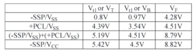
TABLE I
TLPANDESD TESTRESULTS FOR THESSP-ESD DEVICES
[14]. The Vt1of the SSP-ESD device is nearly equal to the Vt1
of the PCL device, but the snapback voltage VSBis smaller than
that of the PCL device. This shows that the triggering device and the SCR of the SSP-ESD device under this stress mode can be turned on in sequence.
The blue-triangle symbols in Fig. 11(a) illustrate the I–V curve of the SSP-ESD device under +TLP/VCCstress mode; it
is parallel to that of the SSP-ESD device under the +TLP/VSS
stress mode. Under the same stress current, the voltage differ-ence for the two different stress modes is about 0.8–1 V, which is equal to one diode operation voltage. In Fig. 3, this voltage difference should result from the diodes between VSSand VCC.
The diodes are the D2 between the two guard rings and the D3 of the PCL device. Excluding the diodes, the I–V curves of the SSP-ESD device under the two stress modes should
be identical. This verifies that the SSP-ESD device during the +ESD/VCC zapping event uses the triggering device and
the SCR as well as the diodes to discharge the ESD current, although there is no direct discharge component for this mode. This is why the It2 values and the HBM and MM threshold
voltages for the two different stress modes are almost the same, as shown in Table I.
The black-square symbols in Fig. 11(b) illustrate the I–V curves of the SSP-ESD device under−TLP/VSSstress events;
they present the typical I–V characteristics of a diode. It starts to turn on and rise exponentially if the applied voltage is larger than the diode turn-on threshold voltage VT. This proves the
discharge components for this stress mode including the NW/p-type substrate diode D0 and the parasitic diode D1 of the triggering device in Fig. 3. In Table I, the It2 value and the
HBM and MM threshold voltages for this mode are slightly larger than those of the (+) PAD-VSSmode.
The blue-circle symbols in Fig. 11(b) illustrate the I–V curve of the SSP-ESD device under the −TLP/VCC stress mode.
It presents the snapback phenomena. The voltages for this stress mode are larger than those of the PCL device under the +TLP/VSSstress mode. Table II lists the critical voltages of the
SSP-ESD device under the−TLP/VSS and−TLP/VCCstress
modes and the PCL device under the +TLP/VSS stress mode
based on the measured results in Fig. 11(b). It can be found that the voltages of the SSP-ESD device under the−TLP/VCC
stress mode is almost equal to the summation voltage of the SSP-ESD device under the−TLP/VSSstress mode and the PCL
device under the +TLP/VSSstress mode. This proves that the
SSP-ESD device can use the PCL device and its diodes D0 and D1 to sink the current for this mode even if there is no direct ESD protection device for this zapping mode. In Fig. 11(b), the It2 value of the PCL device is much larger than that of
diodes D0 and D1 since the PCL device is a huge dimension device compared with the two diodes. Thus, diodes D0 and D1 of the SSP-ESD device will dominate ESD current paths for this zapping mode. This is why It2 values and ESD threshold
voltages of the SSP-ESD device for this mode are almost the same as those of the (−) PAD-VSSmode, as shown in Table I.
Furthermore, 1- and 3-ns very fast TLP stresses on +PCL/VSS are also derived in Fig. 12. We can observed that
Vt1 increases and It2 decreases when the TLP pulsewidth
de-creases. However, It2can reach 1.2 A even when the pulsewidth
is only 1 ns. For the charge-device model, SSP devices can pass +400 and−450 V in the 48-pin dual in-line package and +300 and−350 V in the 208-pin quad flat package.
For shorter pulse durations, by definition, the averaging window is majorly decided by the nonquasi-static region of
Fig. 12. 1- and 3-ns TLP results.
Fig. 13. Scattering-parameter pad set for capacitance measurements.
the pulses. Because, in that region, the SCR has not been fully triggered, the I–V curve will automatically shift toward higher voltages and lower currents.
C. Capacitance of the SSP-ESD Device
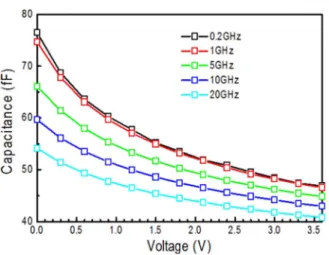
In order to extract the capacitance of the SSP-ESD device, a ground–signal–ground fixture, as shown in Fig. 13, is used as the interface of the SSP-ESD device and the probe tips for HF characteristic measurements. In addition, there are open/short fixtures to eliminate the influence of the transition region between the probe, the probe contact, and the SSP-ESD device. The apparatus to measure the capacitance of the SSP-ESD device is an HP-8510C network analyzer. The measured frequency is from 0.2 to 20 GHz, and the dc reversed-biased voltages are from 0 to 3.6 V.
The measured capacitance decreases as dc voltages and frequencies increase, as illustrated in Fig. 14. Under 0 V and 0.2 GHz, the capacitance value is only 76 fF, which differs from the simulation-program-with-IC-emphasis (SPICE)-simulated values of 78 and 2 fF.
From the SPICE simulations, the estimated capacitance val-ues of the output transistor and the ESD protection devices are 47 and 31 fF, respectively. With such a low capacitance value, the ESD protection devices of the SSP-ESD device still effec-tively can protect the output transistor. The ESD robustness can reach the HBM in 3 kV and the MM in 150 V.
Fig. 14. Total capacitance values of the SSP-ESD device extracted from the HP-8510C network analyzer.
Fig. 15. Test structure and the bias condition for the negative latch-up immunity evaluation of the SSP-ESD device.
D. Latch-Up Immunity for the SSP-ESD Device
For a CMOS IC fabricated on the p-type substrate, the input–output circuits will not suffer the latch-up problem at the positive-charge triggering mode (i.e., the positive charge triggering the p-type substrate) if they are surrounded with a p+ guard ring. It is because the p+ guard ring can effectively suppress the local voltage rise of the p-well potential [19]. The worse case of the latch-up for most ICs is the negative triggering mode [19]. Fig. 15 shows the test structure and the bias condition of the SSP-ESD device for the negative latch-up immunity evaluation. Except for the SSP-ESD device, there are negative triggering node n+ diffusion and grounded p+ diffusion to separate the SSP-ESD device and the negative triggering node. During the negative triggering event, a constant voltage of 2 V is applied to the SCR anode and the drain region of the output transistor. In addition, a negative triggering current is applied to the negative trigger node.
In Fig. 16, IPad, ICC, and ISSare the currents for pad, power
VCC, and ground VSS, respectively. The pad voltage is marked
in VPad. If the NW guard ring is floating, the negative triggering
current I−trican easily drive SSP devices into the latch-up state at 125◦C, as shown in Fig. 16(a). IPad and VPad can be kept
at 0 A and 2 V when the absolute I−tri is below 30 mA. As absolute I−tri increases, IPad jumps from 0 to the clamped
current (100 mA), and VPad falls from 2 to 1.35 V due to the
latch-up occurrence. However, there is no latch-up occurrence on the SSP-ESD device at 125◦C if the NW guard ring connects to 2 V, as shown in Fig. 16(b). Even if absolute I−triramps up
to 100 mA, VPadstill can be kept at a constant voltage of 2 V.
In addition, IPad is still quite low (< 2 mA) since most I−tri
currents flow to the p+ and NW guard rings. The two guard rings can prevent the current flowing into the SSP-ESD device; therefore, the SCR does not enter the latch-up state. This is why the SSP-ESD device not only has the p+ guard ring but also has the NW guard ring. Except the latch-up prevention, the two guard rings are also important for ESD protection. With the two guard rings, the SSP-ESD device can provide a discharge current path for all ESD modes.
IV. CONCLUSION
An SSP scheme is developed and demonstrated to protect the output transistor against ESD damage for Gigahertz ICs. Unlike a self-protection scheme, the output transistor does not need the ballast drain resistor. Unlike the nonself-protection scheme, it does not need the triggering device and any passive component since the output transistor is the triggering device.
Traditionally, the output transistor can turn on and share the ESD current with the ESD device during the whole stress period of the ESD zapping event. Thus, the output transistor should be designed with special layout rules to protect ICs from the ESD damage. This paper has placed the drain region of the output transistor far away from the ESD device; thus, the output transistor can turn off after the ESD device turns on.
REFERENCES
[1] A. Chatterjee and T. Polgreen, “A low-voltage triggering SCR for on-chip ESD protection at ouput and input,” IEEE Elec. Dev. Lett., vol. 12, no. 1, pp. 21–22, Jan. 1991.
[2] B. Van Camp, F. De Ranter, and B. Keppens, “Current detection trigger scheme for SCR based ESD protection of output drivers in CMOS tech-nologies avoiding competitive triggering,” in Proc. 27th EOS/ESD Symp., 2005, pp. 393–399.
[3] C. Russ, M. P. J. Mergens, K. G. Verhaege, J. Armer, P. C. Jozwiak, G. Kolluri, and L. R. Avery, “GGSCRs: GGNMOS-triggered silicon controlled rectifiers for ESD protection for deep sub-micron COMS processes,” in Proc. 23th EOS/ESD Symp., 2001, pp. 23–31.
[4] J. H. Lee, Y. H. Wu, K. R. Peng, R. Y. Chang, T. L. Yu, and T. C. Ong, “The embedded SCR and low capacitance ESD protection device for self-protection scheme and RF application,” in Proc. IEEE Custom Integr. Circuits Conf., 2002, pp. 93–96.
[5] Y. Morishita, “New ESD protection circuits based on PNP triggering SCR for advanced CMOS device application,” in Proc. 24th EOS/ESD Symp., 2002, pp. 6–9.
[6] Y. Morishita and M. Okushima, “A low-leakage SCR design using trigger-PMOS modulations for ESD protection,” in Proc. 29th EOS/ESD Symp., 2007, pp. 376–384.
[7] M. P. J. Mergens, C. Russ, K. G. Verhaege, J. Armer, P. C. Jozwiak, R. Mohn, B. Keppens, and C. S. Trinh, “Diode-triggered SCR (DTSCR) for RF-ESD protection of BiCMOS SiGe HBTs and CMOS ultra-thin gate oxide,” in IEDM Tech. Dig., 2003, pp. 515–518.
analysis,” in Proc. 29th EOS/ESD Symp., 2007, pp. 366–375.
[11] S. Cao, A. A. Salman, J.-H. Chun, S. G. Beebe, M. M. Pelella, and R. W. Dutton, “Design and characterization of ESD protection devices for high-speed I/O in advanced SOI technology,” IEEE Trans. Electron Devices, vol. 59, no. 3, pp. 644–653, Mar. 2010.
[12] M. Shrivastava, H. Gossner, M. S. Baghini, and V. R. Rao, “3D TCAD based approach for the evaluation of nanoscale devices during ESD failure,” in Proc. IEEE ISOCC, 2010, pp. 268–271.
[13] M. Shrivastava, J. Schneider, R. Jain, M. S. Baghini, and H. Gossner, “IGBT plugged in SCR device for ESD protection in advanced CMOS technology,” in Proc. 31th EOS/ESD Symp., 2009, pp. 221–229. [14] J. H. Lee, Y. H. Wu, C. H. Tang, T. C. Peng, S. H. Chen, and A. Oates, “A
simple and useful layout scheme to achieve uniform current distribution for multi-finger silicided grounded gate NMOS,” in Proc. 45th Int. Reliab. Phys. Symp., 2007, pp. 588–589.
[15] H. T. H. Tang, S. C. Huang, S. S. Chen, L. S. Huang, M. C. Wang, and M. C. Jeng, “A novel deep-submicron ESD design margin with TLP,” in Proc. ESA, 2001, pp. 239–244.
[16] J. H. Lee, K. M. Wu, S. C. Huang, and C. H. Tang, “The dynamic current distribution of a multi-finger GGNMOS under high current stress and HBM ESD event,” in Proc. 44th Int. Reliab. Phys. Symp., 2006, pp. 629–630.
[17] B. Van Zeghbroeck, Principles of Semiconductor Devices, Engle-wood Cliffs, NJ, Prentice-Hall, 2007, p. 5.5.5. [Online]. Available: http://ecee.colorado.edu/~bart/book/book/index.html
[18] D. H. Yang, J. F. Chen, J. H. Lee, and K. M. Wu, “Dynamic turn-on mechanism of n-MOSFET under high-current stress,” IEEE Electrturn-on Device Lett., vol. 29, no. 8, pp. 895–897, Aug. 2008.
[19] K. Chatty, P. Cottrell, R. Gauthier, M. Muhammad, F. Stellari, A. Weger, P. Song, and M. Mcmanus, “Model-based guidelines to suppress cable discharge event induced latchup in CMOS ICs,” in Proc. 44th Int. Reliab. Phys. Symp., 2004, pp. 130–134.
Jian-Hsing Lee was the Academician in
Taiwan-Semiconductor Manufacturing Company (TSMC) for “contributions to electrostatic discharge (ESD) protection in CMOS, SOI, image-sensor, SiGe and high voltage technologies” awarded in 2005. He received the M.S. degrees in optic-electron engineer from National Chiao-Tung University, Hsin-Chu, Taiwan, in 1989.
On 1989, he joined TSMC where he worked on reliability analysis of electronic devices. His current interests include ESD, latch-up, nonvolatile semicon-ductor memory devices, reliability physics of VLSI-technology, and device physics. He had served as the program manager of ESD/EOS section in Technology-reliability Physic division of RD organization developing ESD protection for 0.6um-32nm generic CMOS technologies and 1.0um-0.13um high voltage technologies. He has published 32 technical papers in international conferences and Journals, and has granted 198 US patents in the area of CMOS ESD, Latch-up and NVM. He is presently serving as an ESD/EOS consultant for Richtek Technology Corporation and Realtek Semiconductor Corporation.
Ltd., TSMC, Ltd. and NOVATEK, Ltd. As a UMC engineer, he worked on 90nm process ESD solutions at IBM, Fishkill, N.Y. in 2001. Since the end of 2006, he joined eMemory Technology, Taiwan, where he is currently the ESD/ IO department manager. He is the author or coauthor of more than 8 papers published in journals and conferences, and he holds more than 20 patents. His current research interests include ESD/Latch-up devices and circuits, and I/O related circuits.
Hung-Der Su was born in Kaohsiung, Taiwan, on
February 24, 1971. He received the B.S. degree in electrical engineering from Chung Yuan Christian University, Taoyuan, Taiwan, in 1992, M.S. degrees in electrical engineering from the National Taiwan University, Taipei, Taiwan, in 1994, and Ph.D. de-grees in electronics engineering from the National Chiao Tung University, Hsinchu, Taiwan, in 2003.
From 1994 to 2003, he worked at tsmc Ltd., Taiwan. During that period, he worked as product engineer in product department and reliability and circuit engineering department, senior process development engineer in non-volatile memory program, principle engineer in 0.15um logic development program, and technical manager in 90nm logic development program. Since the end of 2003, he joined Richtek Technology Ltd., Taiwan, where he is currently the technology division director. He is the author or coauthor of more than 10 papers published in journals and conferences, and he holds more than 50 patents. His current research interests include HV/UHV devices and ESD/Latch-up devices.
Ke-Horng Chen (M’04-SM’09) received his B.S.,
M.S., and Ph.D. degrees in electrical engineering from National Taiwan University, Taipei, Taiwan, in 1994, 1996, and 2003, respectively.
From 1996 to 1998, he was a part-time IC De-signer at Philips, Taipei. From 1998 to 2000, he was an Application Engineer at Avanti, Ltd., Taiwan. From 2000 to 2003, he was a Project Manager at ACARD, Ltd., where he was engaged in designing power management ICs. He is currently an Associate Professor in the Department of Electrical Engineer-ing, National Chiao Tung University, Hsinchu, Taiwan, where he organized a Mixed-Signal and Power Management IC Laboratory. He is the author or coauthor of more than 100 papers published in journals and conferences, and also holds several patents. His current research interests include power management ICs, mixed-signal circuit designs, display algorithm and driver designs of liquid crystal display (LCD) TV, red, green, and blue (RGB) color sequential backlight designs for optically compensated bend (OCB) panels, and low-voltage circuit designs.
![Fig. 6 shows the cross section and the equivalent circuit of the modified low-voltage-triggered SCR (MLVTSCR) [4]](https://thumb-ap.123doks.com/thumbv2/9libinfo/7887842.155499/3.891.146.361.102.234/shows-section-equivalent-circuit-modified-voltage-triggered-mlvtscr.webp)