A method to characterize the dielectric and interfacial properties of
metal–insulator-semiconductor structures by microwave measurement
Hang-Ting Lue, Tseung-Yuen Tseng, and Guo-Wei Huang
Citation: Journal of Applied Physics 91, 5275 (2002); doi: 10.1063/1.1459603
View online: http://dx.doi.org/10.1063/1.1459603
View Table of Contents: http://scitation.aip.org/content/aip/journal/jap/91/8?ver=pdfcov
Published by the AIP Publishing
Articles you may be interested in
Dielectric properties of MgO-doped compositionally graded multilayer barium strontium titanate films
Appl. Phys. Lett. 92, 072906 (2008); 10.1063/1.2870079
Nondestructive microwave permittivity characterization of ferroelectric thin film using microstrip dual resonator
Rev. Sci. Instrum. 75, 136 (2004); 10.1063/1.1632999
Basic characteristics of metal-ferroelectric-insulator-semiconductor structure using a high- k PrO x insulator layer
J. Appl. Phys. 93, 4137 (2003); 10.1063/1.1558206
Characterization of quality of Ba x Sr 1x TiO 3 thin film by the commutation quality factor measured at microwaves
Appl. Phys. Lett. 81, 1675 (2002); 10.1063/1.1499987
The effect of annealing on the microwave properties of Ba 0.5 Sr 0.5 TiO 3 thin films
Appl. Phys. Lett. 74, 1033 (1999); 10.1063/1.123446
A method to characterize the dielectric and interfacial properties of
metal–insulator-semiconductor structures by microwave measurement
Hang-Ting Lue and Tseung-Yuen Tsenga)
Department of Electronics Engineering and Institute of Electronics, National Chiao-Tung University, Hsinchu, Taiwan, Republic of China
Guo-Wei Huang
National Nano Device Laboratories, Hsinchu, Taiwan, Republic of China
共Received 24 September 2001; accepted for publication 21 January 2002兲
We have developed a method to investigate the dielectric and interfacial properties of gate dielectric thin films by microwave measurement. Ba0.5Sr0.5TiO3共BST兲 thin films were deposited on 10 ⍀ cm 共normal兲 and 10 k ⍀ cm 关high-resistivity, 共HR兲兴 silicon substrates at the same time by rf magnetron sputtering. For the BST/HR-silicon, coplanar waveguides共CPW兲 were fabricated and measured at microwave frequencies with thru-reflect-line calibration while capacitance (C – V) measurements were carried out for BST/normal silicon. From the phase change of CPW transmission line and the maximum capacitance in C – V measurement, the dielectric constants of both the BST thin film and interface layer can be determined. Furthermore, the behaviors of insertion loss versus bias voltage were investigated. The results indicate that our method can provide useful information to study the dielectric and interfacial properties of metal–insulator–semiconductor structures. © 2002 American Institute of Physics. 关DOI: 10.1063/1.1459603兴
I. INTRODUCTION
With the rapid developments of high-k gate dielectrics1 and ferroelectric random access memory,2 the dielectric and interfacial properties of many gate dielectrics deposited on silicon substrate have gained intensive attraction in recent years. Although those metal–insulator–semiconductor共MIS兲 structures have incorporated many high dielectric constant thin films such as ZrTiO4,3 Ta2O5,4 TiO2,5 SrTiO3,6
BaxSr1-xTiO3共BST兲,7,8and SrBi2Ta2O9,9the average
dielec-tric constants of the gate dielecdielec-trics obtained by Cmax
共maxi-mum capacitance or accumulation capacitance兲 in the capacitance–voltage (C – V) measurements are often much lower than measured by metal–insulator–metal capacitors due to the low dielectric constant interface layers. In most cases the oxide dielectrics at the interface diffuse into silicon and form a thin SiO2 layer which lowers down the overall
average dielectric constant. Another possible reason is due to the lattice mismatch of dielectrics and silicon surface, which results in lattice strain and subsequently cause the formation of a thin amorphous layer. Although the interface layer is much thinner than the gate dielectric, the overall capacitance is significantly reduced because the total capacitance is the series combination of the multilayers and will be dominated by the low-capacitance layer. In addition, these interface lay-ers often cause increasing interface trap density and then degrade the performance of the gate dielectrics. Therefore, characterization of the interface layers is the important issue in MIS structure. However, these interface layers are often very thin 共⬍10 nm兲 and their dielectric constants cannot be determined by conventional C – V measurements. Several works10 used multithickness gate dielectrics to estimate the
dielectric constants of the interface layers, assuming both the dielectric constant and thickness of the interface layers were the same for different thickness of the gate dielectrics. How-ever, this assumption is clearly incorrect and only provides a rough estimate. Therefore, additional measurement method for the MIS structure is necessary for exploring its dielectric and interfacial properties.
In our previous work,11 we have developed a technique to measure the dielectric properties of ferroelectric layer de-posited on sapphire by using coplanar waveguide 共CPW兲 with thru-reflect-line共TRL兲 calibration. In this measurement, the propagation constant共or the velocity兲 of the multilayered CPW transmission line is perturbed by the high-dielectric-constant layer and the phase of transmission coefficient, ⌬⌽S21, is changed and can be measured to determine the
dielectric constant of the ferroelectric layer. This phase change is caused by the high dielectric constant layer, that is, thicker film with larger dielectric constant will give the dominant contribution while the thin interface layer with low dielectric constant gives negligible contribution. Contrary to the C – V measurement, this microwave measurement would therefore provide us direct measurement of the dielectric constant of the gate dielectric,d. Afterd is measured, the
dielectric constant of the interface layerican be determined
based on the average dielectric constant averageobtained in
the C – V measurement. Therefore, the dielectric constants of both the gate dielectric thin film and interface layer can be solved. This approach is therefore a useful technique for ex-tracting the dielectric constant of gate dielectric and interface layer accurately.
The microwave properties of BST have been studied by some previous works.12–14Their studies were focused on the applications on the tunable devices in microwave circuits
a兲Electronic mail: [email protected]
5275
0021-8979/2002/91(8)/5275/8/$19.00 © 2002 American Institute of Physics
because BST possessed low-loss and high tunability proper-ties. In this article, we are interested in the dielectric and interfacial properties of (Ba0.5Sr0.5)TiO3共BST兲 thin films
de-posited on silicon substrate. The dielectric constants of both the BST thin film and thin interface layer were measured by the phase response of the CPW transmission lines. The rela-tionships between insertion losses and bias voltages are also investigated and the results clearly imply the correlation with the trap states. For more illustration, polysilicon with high trap densities and thermally grown SiO2were also measured
for comparison. These results imply that CPW transmission lines can be used to investigate the dielectric and interfacial properties of MIS structures.
II. SAMPLE PREPARATION
BST thin films were deposited on 共100兲 n-type silicon substrates with resistivity of ⫽10 ⍀ cm 共normal兲 and ⫽10 k ⍀ cm 关high resistivity 共HR兲兴 by rf magnetron sputter-ing. The deposition conditions of these samples denoted as S1–S7 are listed in Table I. The Ba0.5S0.5rTiO3 target with a
diameter of 3 in. was synthesized using standard solid-state reaction process. Since the microwave loss of the conven-tional silicon substrate共normal兲 with low resistivity is rather high, we employ high-resistivity silicon substrate to carry out this microwave measurement. For consistency, the normal silicon substrate and the high-resistivity silicon substrates were deposited with BST thin films simultaneously on a spin substrate holder in the vacuum chamber. Before the deposi-tion, standard Radio Corporation of America processes were carried out on silicon substrates to remove the native oxide and surface contamination. The deposition temperatures were ranged from 400 to 600 °C. The constant deposition pressure of 5 mTorr which was maintained by a mixture of oxygen and argon mixing ratio 关OMR: O2/(O2⫹Ar)]
ranged from 0% toward 20%. The x-ray diffraction results as
shown in Fig. 1 indicate that all the samples except S6 are well-crystallized films. The thicknesses of BST films were ranged from 500 toward 2000 Å. After deposition, the back-side of the normal substrates were deposited with aluminum for ohmic contact after etching off SiO2 in hydrofluoric
so-lution. Platinum was used as the top electrodes for probe pads. The C – V curves of these MIS capacitors were mea-sured by HP 4284 at 1 MHz.
For the BST/HR-silicon, 1-m-thick aluminum was de-posited on the BST films by thermal evaporator. The photo-lithography and wet etching were then carried out to form the CPW transmission line patterns as indicated in Fig. 2. The center conductor width 共S兲 was designed to be 20 m and the gap width 共W兲 10 m. Because the characteristic impedance of the CPW transmission line can be changed by the dielectric layer, impedance mismatch may happen. In ad-dition, the transition between the pads and the narrow CPW
FIG. 1. X-ray diffraction patterns of BST films indicated. TABLE I. Sample descriptions and the measurement results.
Sample name HR共bare substrate兲 S1 共BST兲 S2 共BST兲 S3 共BST兲 S4 共BST兲 S5 共BST兲 S6 共BST兲 S7 共BST兲 Samples descriptions and the deposition conditions OMR: O2/共O2⫹Ar兲 ¯ 0% 10% 20% 10% 10% 10% 10% Deposition temperature共°C兲 ¯ 600 600 600 600 600 400 500 td共Å兲 ¯ 1100 1200 1150 550 2350 1000 1100 ti共Å兲 ¯ 50 40 50 50 60 110 50 Microwave measurement q2 ¯ 7.5⫻10⫺3 8.1⫻10⫺3 7.8⫻10⫺3 3.9⫻10⫺3 1.6⫻10⫺2 7.2⫻10⫺3 7.5⫻10⫺3 q3 ¯ 7.2⫻10⫺3 7.8⫻10⫺3 7.5⫻10⫺3 3.6⫻10⫺3 1.5⫻10⫺2 6.5⫻10⫺3 7.2⫻10⫺3 ⌬⌽(S21) ¯ 32.3° 31.9° 33.8° 18.7° 55.9° 9.3° 24.1° eff 6.291 7.691 7.675 7.759 7.078 8.831 6.925 7.324 C – V Cmax共pF兲 ¯ 765 567 609 690 537 348 626 measurements average ¯ 103 83 86 49 152 45 85 Calculated d ¯ 185 169 187 187 167 85 134 results i ¯ 10 5 6 5 31 9 9 a
Sample P: SiO2共1000 Å兲/polysilicon/HR–Si, deposited by PEVCD in continuous sequence. bSample X1: SiO
2共1000 Å兲/HR–Si, deposited by thermal growth at 1000 °C. cSample X2: SiO
2共1000 Å兲/HR–Si, deposited by thermal growth at 1000 °C with SiO2in the gap共W兲 removed. dFor the MIS capacitors, the areas are defined to be 9.6⫻10⫺4cm2.
5276 J. Appl. Phys., Vol. 91, No. 8, 15 April 2002 Lue, Tseng, and Huang
transmission lines 共tapers兲 also causes parasitic effect. The TRL calibration was employed to de-embed the microwave response accurately. Details of TRL calibration have been described previously.11,15 After TRL calibration, the effects of parasitic reflection and impedance mismatch are removed. We designed and measured the ‘‘thru,’’ ‘‘reflect,’’ and ‘‘line’’ CPW patterns at the same wafer, as shown in Fig. 2, and then calculated the TRL calibration by a self-made program. The line pattern was 5 mm longer than the thru, hence, the S-parameter de-embedded by the TRL calibration is equiva-lent to 5 mm long CPW transmission line. These CPW de-vices were measured at Cascade microwave probe station with HPC GSG probes, and the S parameters were measured by the network analyzer HP 8510C with frequency ranging from 200 MHz to 20 GHz. Before measurements, full-two port calibrations were conducted with standard kits to re-move external systematic errors.
In order to investigate the behavior of charge carriers in the MIS structures, dc voltage bias was applied at the center conductor through a bias tee. The two ports were applied with the same voltage synchronously to prevent current flow. The measurement frequency was fixed at 20 GHz and the voltage is swept from⫹5 to ⫺5 V. For each CPW device the sweep-frequency measurement at zero bias was first per-formed, and then the sweep-bias measurement at 20 GHz was then carried out without lifting the probes. The sweep-bias measurement also incorporated TRL calibration for con-sistency.
The film thickness of the gate dielectrics was obtained by the spectrophotometer 共n&k analyzer 1200, Nikon兲. The n&k analyzer incorporates the Forouhi–Bloomer16 formula-tion for optical constants along with a parameterized model for multilayer configuration. The thickness of the thin inter-face layers were observed by transmission electron micro-scope 共TEM兲 with Philips Tecnai 20 microscope that was operating at an accelerating voltage of 200 keV.
The samples P, X1, and X2 were prepared for compari-son. For sample P, 3000-Å-thick poly-silicon was deposited directly on HR-silicon substrate, after that 1000-Å-thick SiO2layer was deposited. The processes were done in a
con-tinuous sequence by plasma enhanced chemical vapor depo-sition共PECVD兲. For samples X1 and X2, 1000-Å-thick SiO2
was thermally grown at 1000 °C in O2 ambient. For the
sample X2, SiO2in the gap共W兲 was removed by dipping the
sample in the buffer oxide etcher 共BOE, NH4F: HF⫽6:1兲
with photoresist covered on the aluminum conductors. CPW patterns were also fabricated on these samples to compare with the BST gate dielectrics.
III. MICROWAVE ANDC – V MEASUREMENTS OF THE DIELECTRIC CONSTANT
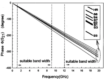
The plots of phase of transmission coefficients, S21,
measured at zero gate bias versus frequency are shown in Fig. 3. We can observe that the phase of CPW transmission lines is changed after deposition of BST thin film on silicon substrate. These phase changes with respect to the bare HR-silicon substrate, denoted by ⌬⌽S21 are listed in Table I,
which are around 10° to 60° at 20 GHz. It is indicated that the phase change is a function of deposition condition and thickness of the BST thin film. For each sample, the effective dielectric constanteffis extracted by the phase of
transmis-sion coefficient S21:
兩⌽S21兩⫽
360
冑
efffl
c 共degree兲, 共1兲
where f is the frequency, c is the velocity of light, and
l
is the length of transmission line, and is equal to 5 mm. TheFIG. 2. 共a兲 Cross-section view of CPW transmission lines structures. 共b兲 Layouts of thru, reflect, and line.
FIG. 3. The phase of S21of BST/HR–Si CPW transmission lines共5 mm
long兲 measured at zero gate bias after TRL calibration.
TRL calibration is not suitable for frequencies near n/2 共or equivalent 0° and 180° phase shifts兲. Therefore, the suitable bandwidths without these points are shown in Fig. 3. It is indicated that the phases of all CPW transmission lines are straight lines implying that the dielectric constants of BST films are constant over this frequency range. The effective dielectric constants eff are extracted by the slopes of those
lines in Fig. 3.
The effective dielectric constanteff is a measure of the
microwave propagation velocity. We have developed the cal-culation procedure in our previous work11 for the two-layer structure, and we can simply extend the formula to three-layer structure with the same conformal mapping method11,17,18 as the following:
eff⫽1⫹q1共Si⫺1兲⫹q2共i⫺Si兲⫹q3共d⫺i兲, 共2兲 and k0⫽ S S⫹2W, 共3兲 k1⫽ sinh共S/4h兲 sinh关共S⫹2W兲/4h兴, 共4兲 k2⫽ sinh关S/4共td⫹ti兲兴 sinh关共S⫹2W兲/4共td⫹ti兲兴 , 共5兲 k3⫽ sinh关S/4td兲 sinh关共S⫹2W兲/4td兴 , 共6兲 qi⫽ 1 2 K共ki兲 K
⬘
共ki兲 K⬘
共k0兲 K共k0兲 , i⫽1,2,3, 共7兲where h, td, and ti are defined to be the thickness of sub-strate, gate dielectric, and interface layer, respectively. Si,
d, and i are the dielectric constants of the Si substrate,
gate dielectric, and interface layer, respectively. K(x) is the elliptical integral of the first kind, and K
⬘
(x)⬅K(冑
1⫺x2) qiare the filling factors. The parameters are clearly defined in Fig. 2. Equation共2兲 can be rewritten as
eff⫽共1⫺q1兲⫹共q1⫺q2兲Si⫹共q2⫺q3兲i⫹q3d. 共8兲
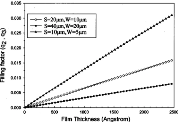
Equation 共8兲 indicates that the total effective dielectric constant is the sum of the dielectric constant of each layer multiplied by the filling factor. In other words, the filling factor is a measure of the proportionality of electromagnetic energy inside each layer. The filling factor of the substrate, q1, is almost a constant and approaches 0.5. For our CPW devices with S⫽20 m, W⫽10m, the filling factors. q2 and q3 are calculated versus various film thicknesses and plotted in Fig. 4. For comparison, filling factors for different linewidths CPW are also shown. Note that the filling factor is almost proportional to the film thickness and increases with shorter linewidths. The effective dielectric constants were measured for each sample and the corresponding q2 and q3
are listed in Table I.
Note that the thin interface layers are less than 100 Å, and the corresponding filling factors, (q2⫺q3), are less than
7⫻10⫺4. Furthermore, the dielectric constant of the inter-face layer is much lower than that of the gate dielectric,
therefore the contribution of interface layer is estimated to be less than 1% and can be neglected for convenience. We can simplify the Eq.共2兲 to
eff⫽1⫹q1共Si⫺1兲⫹q2共d⫺Si兲. 共9兲
This equation is consisted of only one unknown value, d, and hence the gate dielectric constant can be extracted
directly by the microwave measurements. If Eq. 共2兲 rather than Eq. 共9兲 is used, the two unknown values d and i
should be determined if combined with Eq. 共10兲, which will be discussed next.
For a 1000-Å-thick thin film, its filling factor q3 is
around 0.007, therefore high dielectric constant thin film is required to give sensitive phase change of CPW transmission line. That is the reason why we use BST with high dielectric constant (d⬎200) to demonstrate this technique. However,
for thinner gate dielectrics with lower dielectric constants, the phase changes can be too small to be measured. In this case, it can be solved by reducing the linewidths of CPW transmission lines. As indicated in Fig. 4, we can find that the filling factor increases significantly with reducing line-width. The measurement sensitivity can be enhanced by re-ducing the linewidth. Another possible way to enhance the phase change is to increase the length of transmission line. However, in these cases the insertion losses increase corre-spondingly, and the etching process becomes more difficult. Therefore, certain trade-off between the linewidth and phase change should be made to ensure good-sensitivity measure-ment.
The measurement of insertion loss versus frequency for several samples was carried out and shown in Fig. 5. It shows that the loss of passivated polysilicon is the lowest while that of the thermal oxide is the largest. The reason for this phenomenon will be discussed in Sec. V.
The results of C – V measurements of several samples are shown in Fig. 6. The average dielectric constant is equal to the series combination of the capacitances of BST and interface layer, and can be calculated by
average⫽ Cmax共td⫹ti兲 A0 ⫽
冉
td d⫹ ti i冊
⫺1 共td⫹ti兲, 共10兲FIG. 4. Calculated filling factors vs BST film thickness for various CPW linewidths indicated.
5278 J. Appl. Phys., Vol. 91, No. 8, 15 April 2002 Lue, Tseng, and Huang
where Cmax is the maximum capacitance共or the
accumula-tion capacitance兲. A is the capacitor area, which is equal to 9.6⫻10⫺4 cm2 in our measurement. 0 is the free space
dielectric permittivity. This average dielectric constant is of-ten much lower (average⬍100) than the dielectric constant
d measured by microwave CPW transmission lines.
Com-bining Eqs.共10兲 and 共2兲, we can calculate dandi, and the
results are listed in Table I. For simplicity, Eq.共9兲 instead of Eq. 共2兲 can be used and the results provide less than 1% deviation, indicating that the contribution of interface layer to the microwave measurements is negligibly small
IV. DISCUSSION OF THE DIELECTRIC PROPERTIES OF BSTÕSI
As indicated in Table I, thei range from 5 toward 31,
which are much lower thand, but larger than 3.9共dielectric constant of SiO2). The lattice constant of cubic BST can be calculated by x-ray spectrum shown in Fig. 1 and the results show that the lattice constant of BST is 3.97 Å, which is much lower than that of the silicon, 5.40 Å. This lattice mismatch between BST and silicon wafer may lead to thin
interface layer formed to compensate the lattice strain. The interface layer of sample S1 is clearly viewed by TEM pic-tures shown in Fig. 7, from which the thickness of the inter-face layer of sample S1 is obtained to be 5 nm. Typical depth profile analyzed by the secondary ion mass spectroscopy of sample S1 共Fig. 8兲 indicates uniform concentration distribu-tion for all species in the film, but atoms accumulate at the interface of BST/silicon. Although it is common to assume the interface layer of gate dielectric is pure SiO2, this
as-sumption is incorrect because Ba, Sr, and Ti ions can diffuse into SiO2 interface layer. Small ions such as Ti⫹4 共0.6 Å兲
show a large accumulation at the interface, indicating that
FIG. 5. The insertion loss vs frequency for various samples indicated, which was measured at zero bias after TRL calibration.
FIG. 6. C – V characteristics of Pt/BST/Si共normal兲 MIS structures.
FIG. 7. Transmission electron microscope picture of sample S1. The upper side is silicon, while the lower side is BST thin film.
FIG. 8. Secondary ion mass spectroscopy depth profile for S1.
Ti⫹4ions easily diffuse into the interfacial SiO2 layers
com-pared to Ba and Sr. This BST diffused SiO2layer has
dielec-tric constant larger than that of SiO2, 3.9.
One important result of our method is that we can obtain the dielectric constants of both the BST film and interfacial layer. The dielectric constant d of 600 °C deposited BST
film is around 200 and decreases for lower deposition tem-perature共samples S2, S6, and S7兲. d is only 85 for 400 °C
deposition temperature 共S6兲, this is because that the BST layer is amorphous at low temperature growth, as confirmed by the weak peak intensity in the x-ray spectrum 共Fig. 1兲. The average dielectric constants average decrease with de-creasing film thickness 共samples S2, S4, and S5兲, which is common result in the high-k gate dielectrics. On the other hand, we can observe the dielectric constantdof BST layer and the interface layer thickness ti do not change much for
different BST film thickness and the average dielectric con-stants are lowered down much more for thinner BST films. Therefore, it may conclude that the decreasing average di-electric constant with decreasing thickness is mainly due to the interface layer rather than the crystallinity of BST layer in this case. In addition, the interface layer dielectric constant iincreases with increasing BST film thickness. This may be
attributed to the better crystallized interface layer for thicker BST film.
So far we are the first to measure the dielectric constants of both the gate dielectrics and interface layers directly by employing conventional C – V and microwave measurements together. This measurement technique would provide very useful information for the MIS structure studies.
V. THE MICROWAVE RESPONSE OF MULTILAYERED CPW TRANSMISSION LINES UNDER BIAS
The phase of S21 is related to the dielectric constant of
the thin film. On the other hand, the magnitude of S21 共or
insertion loss兲 is able to give us the information about the charge carrier. We can apply dc bias on the center conductor in the CPW transmission line to attract charge carriers into the interface and monitor the change of insertion loss. For n-type substrate, there is electron accumulation at the surface for positive gate bias while there is hole inversion for nega-tive bias. In both cases, we may expect that the charge accu-mulation in the interface of BST/Si will cause dissipation of electromagnetic energy. The results of the measurements of insertion loss versus bias at 20 GHz for various samples are shown in Figs. 9–12. On the basis of these results, we can find that the insertion loss does not always change rapidly with the bias but instead there are voltage ranges existed with small variations of insertion loss in some samples. In this region the insertion losses vary slowly and beyond this region the insertion losses increase rapidly. We believe that this interesting phenomenon is related to the interface traps. If the charge carrier density Q (1/cm2) attracted by the bias is less than the trap density, Qt, the charge carriers will be
bound in the trap states. The trap states are the localized electronic energy states or in other words, the carriers in the trap states are immobile. Therefore, those charge carriers will contribute much less microwave dissipation. In this way, the
trap states effectively ‘‘pin’’ the Fermi level and the micro-wave dissipation shows low variation in this voltage range. However, if the applied bias is larger such that Q⬎Qt, the
additional carriers will go to the conduction bands or valence bands and consequently contribute larger microwave dissipa-tions. Since the energy of the trap states is often continuously distributed in the band gap, the trap densities are often char-acterized by energy density of states, Dit(1/ cm2eV). The Dit
then causes less band bending than ideal, and the slope of the insertion loss versus bias is reduced.
Based on the earlier argument, we can qualitatively ex-plain the characteristics of the behavior of insertion loss ver-sus bias voltage. As shown in Fig. 9, 10% OMR BST 共S2兲 has the fastest variation implying that lower trap density ex-isted in this sample compared to those of S1 and S3. In Fig. 10, the low temperature grown BST共S6兲 has smaller varia-tion implying larger trap densities existed in this sample. In Fig. 11, thinner BST gate dielectrics共S4 and S2兲 have faster variations because their capacitances are larger such that the charge densities attracted per unit voltage are larger. For more illustration, characteristics of passivated polysilicon
FIG. 9. Comparison of the insertion losses vs bias at 20 GHz for samples deposited at various oxygen mixing ratio.
FIG. 10. Comparison of the insertion losses vs bias at 20 GHz for samples deposited at various temperatures.
5280 J. Appl. Phys., Vol. 91, No. 8, 15 April 2002 Lue, Tseng, and Huang
were also measured 共sample P兲. The 3000-Å-thick poly-silicon film was used to provide trap states while the 1000-Å-thick SiO2was used for isolation and passivation. Gamble
et al.19 have pointed out the incorporation of polysilicon on the surface of HR silicon will reduce the microwave loss through trap states; We are now verifying this assumption by applying bias. In Fig. 12, the insertion loss of sample P re-mains almost constant for various biases, indicating that all the carriers induced by the applied bias were accommodated in the trap states. This result strongly suggests the correlation of the behavior of insertion loss with trap states. For the 1000-Å-thick thermal-oxide共sample X1兲 the insertion loss is larger than sample P, and shows a larger variation over bias. The reason for that the incorporation of insulating oxide would cause large microwave loss was explained by Wu et al.20 That is, there is surface band bending existed at the interface of silicon substrate due to the oxide fixed charge. This band bending causes a conducting channel between the signal and ground lines and contributes a large microwave loss. The insertion loss of sample X2 in which the SiO2 in
the gap of CPW was removed is reduced 共Fig. 12兲 because the conducting channel in the gap was removed. The inser-tion loss of sample X2 also shows a small variainser-tion over bias. This is due to the accumulated carriers below the con-ductors.
Another interesting behavior is the phase changes, as shown in Fig. 13, indicating the phases⌽S21remain constant
for small bias voltages, as the results in the measurement of insertion loss共Fig. 9兲. Beyond this region, the phase changes increase indicating a slower microwave velocity. This behav-ior is due to the ‘‘slow wave’’ phenomenon.21–23The accu-mulated free carriers not only increase the loss but also ef-fectively slow down the microwave velocity. At low bias voltages, the carriers are trapped in the trap states and are immobile. Therefore, the slow-wave property does not occur. For accurate measurement of the dielectric constant, the phase should be chosen in the range with low variation to prevent the effect of slow wave.
Although we can qualitatively explain the behavior of insertion loss over bias, the accurate modeling of the MIS CPW transmission lines is complex and requires more rigor-ous analysis of the distribution of charge carriers. It needs further study to quantitatively characterize these phenomena. By the earlier-mentioned result of this article, the appli-cation of passivated polysilicon is a good choice to keep the HR silicon low-loss, even for high bias voltage. We also suggest deep-level traps introduced by ion implantation into the HR-silicon surface will result in the similar behavior due to the pinning of the deep level. All these trap states can be monitored by the relationships of insertion loss versus bias voltage.
High-resistivity silicon is thought to be a possible candi-date for rf-complementary metal–oxide–semiconductor 共CMOS兲 substrate. Recent developments of silicon-based rf– CMOS meet difficulty24 due to the loss of silicon substrate. Conventional CMOS silicon substrate (⬇1˜0⍀-cm) is high loss, which causes serious parasitic effects both in the active 共CMOS, BJT, etc.兲 and passive devices 共inductors, transmis-sion lines, etc.兲. To overcome such high loss, developments such as microelectromechanical technology25 and thick
FIG. 11. Comparison of the insertion losses vs bias at 20 GHz for samples with various film thicknesses.
FIG. 12. Comparison of the insertion losses vs bias at 20 GHz for several samples indicated.
FIG. 13. Comparison of the phase changes vs bias at 20 GHz for several samples indicated.
polymides26 have been incorporated. However, those tech-nologies are not fully compatible with standard CMOS pro-cess and there are also problems in the propro-cess yield. These drawbacks are expected to be overcome by employing HR-silicon substrate. If epilayer with doping can be grown on the HR-silicon wafer or by ion implantation, then active devices can be fabricated. For the passive devices such as inductors, one can incorporate HR-silicon substrate with passivated polysilicon or deep level implanted, and the quality factor共Q value兲 of the devices can be increased. These fabrication processes are all under the standard CMOS process without changing too much. Therefore HR silicon may be used as the rf–CMOS substrate to reduce the substrate parasitic effects and increase the performance of microwave devices.
VI. CONCLUSIONS
In conclusion, we present an attempt to measure both the dielectric and interfacial properties of MIS structures by CPW transmission lines. According to the phase changes and C – V measurements, the dielectric constants of both the gate dielectrics and thin interface layers can be determined accu-rately with TRL calibration. This method provides a useful technique for material characterization.
The behavior of insertion loss versus bias shows obvious correlations with the trap states. We have demonstrated sev-eral phenomena and given qualitative analysis. Although there remain some problems for accurate modeling, we be-lieve this technique provide some information about the MIS structures.
ACKNOWLEDGMENTS
The authors gratefully acknowledge the financial support from the National Science Council of Republic of China un-der Contract NO. NSC 89-2212-E009-081. Dr. Sz-Chian Liou in the department of material science and engineering in National Chiao-Tung University is appreciated for his help with TEM measurements.
1G. D. Wilk, R. M. Wallace, and J. M. Anthony, J. Appl. Phys. 89, 5243
共2001兲.
2E. Tokumitsu, R. I. Nakamura, and H. Ishiwara, IEEE Electron Device
Lett. 18, 160共1997兲.
3
D. A. Chang, P. Lin, and T. Y. Tseng, J. Appl. Phys. 78, 7103共1995兲.
4H. F. Luan, S. J. Lee, C. H. Lee, S. C. Song, Y. L. Mao, Y. Senzaki, D.
Roberts, and D. L. Kwong, Tech. Dig. - Int. Electron Devices Meet. 1999, 141共1999兲.
5X. Guo, X. Wang, Z. Luo, T. P. Ma, and T. Tamagawa, Tech. Dig. - Int.
Electron Devices Meet. 1999, 137共1999兲.
6
K. Eisenberg et al., Appl. Phys. Lett. 76, 1324共2000兲.
7A. Srivastava, V. Craciun, J. M. Howard, and R. K. Singh, Appl. Phys.
Lett. 75, 3002共1999兲.
8
S. Jun, Y. S. Kim, J. Lee, and Y. W. Kim, Appl. Phys. Lett. 78, 2542 共2001兲.
9
E. Tokumitsu, G. Fujii, and H. Ishiwara, Jpn. J. Appl. Phys., Part 1 39, 2125共2000兲.
10S. Otani, M. Kimura, and N. Sasaki, Appl. Phys. Lett. 63, 1889共1993兲. 11
H. T. Lue and T. Y. Tseng, IEEE Trans. Ultrason. Ferroelectr. Freq. Control
48, 1640共2001兲.
12J. F. Scott, D. Galt, J. C. Price, J. A. Beall, R. H. Ono, C. A. P. Dearaujo,
and L. D. Mcmillan, Integr. Ferroelectr. 6, 189共1995兲.
13J. F. Scott, Ferroelectric Memories共Springer, Berlin, 2000兲, Chap. 13. 14F. A. Miranda, F. W. Van Keuls, R. R. Romanofsky, C. H. Mueller, and J.
D. Warner, Integr. Ferroelectr. 34, 247共2001兲.
15G. F. Engen and C. A. Hoer, IEEE Trans. Microwave Theory Tech. 27,
897共1979兲.
16A. R. Forouhi and I. Bloomer, Phys. Rev. B 38, 1865共1988兲.
17E. Carlsson and S. Gevorgian, IEEE Trans. Microwave Theory Tech. 47,
1544共1999兲.
18C. M. Jackson, T. Pham, Z. Zhang, A. Lee, and C. Pettiete-Hall, IEEE
MTT-S Int. Microwave Symp. Dig. 3, 1439共1995兲.
19
H. S. Gamble, B. M. Armstrong, S. J. N. Mitchell, Y. Wu, V. F. Fusco, and J. A. C. Stewart, IEEE Microwave Guid. Wave Lett. 9, 395共1999兲.
20
Y. Wu, H. S. Gamble, B. M. Armstrong, V. F. Fusco, and J. A. C. Stewart, IEEE Microwave Guid. Wave Lett. 9, 10共1999兲.
21J. P. K. Glib and C. A. Balanis, IEEE Trans. Microwave Theory Tech. 40,
2148共1992兲.
22E. S. Tong and S. K. Chaudhuri, IEEE Trans. Microwave Theory Tech. 47,
1760共1999兲.
23
S. Chen, R. Vahldieck, and J. Huang, IEEE Trans. Microwave Theory Tech. 44, 2487共1996兲.
24T. H. Lee and S. S. Wong, Proc. IEEE 88, 1560共2000兲.
25V. Milanovic, M. Gaitan, E. D. Bowen, and M. E. Zaghloul, IEEE
Micro-wave Guid. Wave Lett. 6, 380共1996兲.
26
G. E. Ponchak, A. Margomenos, and L. P. B. Katehi, IEEE Trans. Micro-wave Theory Tech. 49, 866共2001兲.
5282 J. Appl. Phys., Vol. 91, No. 8, 15 April 2002 Lue, Tseng, and Huang