Memory Effect of Oxide
ÕOxygen-Incorporated
Silicon Carbide
ÕOxide Sandwiched Structure
T. C. Chang,a,b,
*
,zP. T. Liu,c,dS. T. Yan,eF. M. Yang,eand S. M. Szed,e aDepartment of Physics and Institute of Electro-Optical Engineering, National Sun Yat-Sen University, Kaohsiung, TaiwanbCenter for Nanoscience and Nanotechnology, National Sun Yat-Sen University, Gushan Chiu, Kaohsiung 804, Taiwan
cDepartment of Photonics and Display Institute, National Chiao Tung University, Hsin-Chu, Taiwan dNational Nano Device Laboratory, Hsin-Chu 300, Taiwan
e
Institute of Electronics, National Chiao Tung University, Hsin-Chu, Taiwan
The memory effects of the oxide/oxygen-incorporated silicon carbide共SiC:O兲/oxide sandwiched structure were investigated. The memory window is decreased with the increasing of the oxygen content in the SiC:O film due to the reduction of dangling bonds. A concise model is proposed to explain the reduction of dangling bonds with increasing oxygen content. Also, a higher breakdown voltage is observed with less oxygen content in the SiC:O film, which is attributed to the high barrier height induced by electron trapping in the SiC:O film.
© 2005 The Electrochemical Society. 关DOI: 10.1149/1.1850859兴 All rights reserved.
Manuscript submitted February 16, 2004; revised manuscript received July 30, 2004. Available electronically January 12, 2005.
The Semiconductor Industry Association 共SIA兲 International Technology Roadmap for Semiconductors共ITRS兲 indicates the chal-lenge, beyond the year 2005, for nonvolatile semiconductor memo-ries is to achieve reliable, low-power, low-voltage performance.1In the area of electrically erasable programmable read-only memory 共EEPROM兲 semiconductor devices, there are essentially two domi-nant technologies which compete for an ever-expanding world mar-ket: (i) floating-gate EEPROMs and (ii) floating-trap SONOS, his-torically metal-insulator-SiO2-Si共MIOS兲 EEPROMs. To date, mass-produced nonvolatile memory devices are based on the concept of a continuous layer of floating gate.2However, it has faced the diffi-culties of consecutive scaling down due to the compromise between long-term nonvolatility and high operating speed.3 Recently, the concept of distributed storage of charge by an insulator, such as nitride layer, has caught much attention.4Among several kinds of MIOS memory devices, silicon nitride, as the charge-trapping insu-lator in the MIOS structure, is most widely used.5Other insulators are investigated to replace the silicon nitride film, such as titanium oxide, tantalum oxide, and aluminum oxide. However, these mate-rials cannot offer sufficient storage centers for the consideration of a large memory window. Therefore, the MIOS device has been made by metal ion implantation共e.g., Au兲 into SiO2to form the interfacial charge-storage centers.6Also, to prevent the carriers from injecting into the charge-trapping insulating film from the gate, not from the channel, a blocking oxide is regularly used to cap-on the insulator film, which forms an oxide/insulator/oxide sandwiched structure.7,8 In this contribution, a novel metal-oxide insulator oxide silicon 共MOIOS兲 gate stack was investigated. The memory effects of the oxide/SiC:O/oxide sandwiched structure were demonstrated, which can be utilized as a high-performance MOIOS memory device.
Experimental
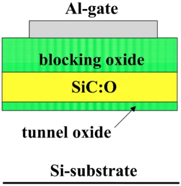
Figure 1 shows the device structure in this study. First, a 2 nm thick thermal oxide was grown on p-type共100兲 6 in. Si substrate by dry oxidation in an atmospheric pressure chemical vapor deposition 共APCVD兲 furnace as a tunnel oxide layer. Subsequently, a 20 nm SiC:O layer was deposited by high-density plasma chemical vapor deposition 共HDP-CVD兲 on the tunnel oxide as a charge-trapping layer, followed by the deposition of a 20 nm HDP-CVD silicon dioxide as the blocking oxide. A steam densification at 982°C was also performed for 180 s to densify the blocking oxide.8The depo-sition of the SiC:O film was kept at 350°C in a low pressure of 3
mTorr with precursors of SiH4, CH4, and O2 and an inductively coupled plasma共ICP兲 power of 900 W. The parameters of the depo-sition of the SiC:O film are listed in Table I. This study was divided into three samples. The deposition of SiC:O with least oxygen con-tent共2 sccm兲 was defined as sample 1. From sample 1 to sample 3, the content of oxygen was increased with a decreased refractive index. The low pressure of 3 mTorr during deposition makes the path length an electron travels without undergoing a collision with a gas atom共or mean-free path兲 increased, which improves the unifor-mity of the thin film.9The blocking oxide was deposited at 350°C with the ratio of SiH4:N2O⫽ 6 sccm:150 sccm and a 900 W ICP power. Finally, the Al gate electrode was patterned and sintered to form a MOIOS structure.
Results and Discussion
To study memory effects of the oxide/SiC:O/oxide sandwiched structure, a bidirectional voltage sweeping between 7 and (⫺7) V
*Electrochemical Society Active Member.
zE-mail: [email protected] Figure 1. The structure of the MOIOS device shown in this work. Journal of The Electrochemical Society, 152共2兲 G144-G147 共2005兲
0013-4651/2005/152共2兲/G144/4/$7.00 © The Electrochemical Society, Inc.
G144
) unless CC License in place (see abstract).
ecsdl.org/site/terms_use
address. Redistribution subject to ECS terms of use (see
140.113.38.11
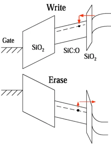
was performed. Figure 2 shows the capacitance-voltage共C-V兲 hys-teresis in this study for different samples. It is clearly observed that as the content of oxygen is increased, the threshold voltage shift 共memory window兲 is decreased from sample 1 to sample 3. The memory window of sample 1 is estimated to be about 1.1 V under 7 V operation. In Fig. 3 the band diagrams of the ‘‘write’’ and ‘‘erase’’ operation are exhibited. When the MOIOS structure is operated un-der positive polarity, the electrons directly tunnel from the Si sub-strate through the tunnel oxide and are trapped in the forbidden gap of the SiC:O layer. When the device is negatively operated, the electrons may tunnel back to the Si substrate through tunnel oxide. The different threshold voltages before and after programming can be defined as ‘‘1’’ or ‘‘0’’ for a memory device. The blocking oxide is utilized to prevent the carriers of gate electrode from injecting into the charge-trapping layer by Fowler-Nordheim共F-N兲 tunneling. HDP-CVD SiC:O is produced in a high-density-plasma chamber with a 900 W ICP power. The radio frequency共rf兲 ICP power is used to increase the spiral motion of the charged particle. A charged par-ticle gains more energy the more times it moves around the spiral and a high-density plasma is produced.9During the deposition of the carbide layer, the simultaneously slight etching due to the bombard-ment of the high-density plasma is processed, which forms a densi-fied and trap-rich layer and contributes a larger memory window than other processes to fabricate the SiC:O film.9,10
To investigate the influence of the oxygen content on the memory window, as shown in Fig. 4, Fourier transform infrared spectroscopy共FTIR兲 was performed. Figure 5a and b exhibits the bonding types of Si-C and Si-H, respectively.11In Fig. 4 and 5, as the oxygen content is increased, the absorbance of Si-O bond is obviously increased and that of both Si-C and Si-H bonds is de-creased. We proposed a model to describe the structural formula of
the SiC:O film during deposition in Fig. 6. A trap-rich SiC:O film is composed of Si-O, Si-C, C-H, and Si-H bonds, and the dangling bonds, a charge-trapping site, are attributed to the weak Si-H bonds which are easily broken and the C-H bonds which are not well-bound, as the dotted line shown in Fig. 6. As the content of oxygen
Table I. The parameters of the deposition of the SiC:O films.
SiH4共sccm兲 CH4共sccm兲 O2共sccm兲 Refractive index
Sample 1 12 12 2 1.669
Sample 2 12 12 5 1.592
Sample 3 12 12 8 1.483
Figure 2. The C-V hysteresis for different samples under 7 and (⫺7) V
bidirectional voltage sweeping.
Figure 3. The band diagrams of the ‘‘write’’ and ‘‘erase’’ operation.
Figure 4. FTIR spectrum of the deposited SiC:O film.
Journal of The Electrochemical Society, 152共2兲 G144-G147 共2005兲 G145
) unless CC License in place (see abstract).
ecsdl.org/site/terms_use
address. Redistribution subject to ECS terms of use (see
140.113.38.11
is increased, Si-H bonds may be easily broken by oxygen and the oxygen atoms bind with the Si dangling bonds to form the strong Si-O bonds. Also, the increased oxygen reacts with part of the Si-C and C-H bonds to form the volatile CO compound, which makes the dangling bonds decreased. It is inferred that the magnitude of the memory window of the oxide/SiC:O/oxide sandwiched structure is in accordance with the amount of dangling bonds. A smaller memory window is attributed to fewer charge-trapping sites with more oxygen content.
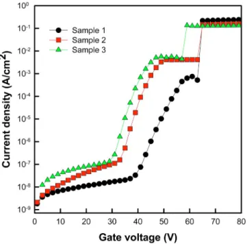
Figure 7 shows the C-V characteristics of the oxide/SiC:O/oxide sandwiched structure. All the samples retain good leakage charac-teristics at the high voltage of 30 V. For sample 1, the breakdown
voltage is up to 40 V. Also, it is clearly observed that the breakdown voltage is decreased with the increased content of oxygen. As shown in the band diagram of Fig. 8, when electrons are captured in a charge-trapping layer with rich charge-trapping sites,12the conduc-tion band of the charge-trapping layer is lifted, which forms an energy barrier for conductive electrons. If more electrons are trapped in the SiC:O film, a higher barrier is generated, which re-sults in lower leakage current and higher breakdown voltage of the gate-stacked structure. Therefore, the SiC:O film with less oxygen content contributes to a larger memory window and a higher break-down voltage, demonstrating the reliable characteristics as a candi-date for use of future MOIOS nonvolatile memory devices.
Figure 5. 共a兲 The FTIR absorbance of Si-C bonds and 共b兲 FTIR absorbance
of Si-H bonds.
Figure 6. The structural formula of the proposed model. As the oxygen
content is increased, both Si-C and Si-H bonds may be decreased, which renders the decrease of the dangling bonds. The dotted lines indicate the dangling bonds of the C-H bonds which are not well-bound.
Figure 7. The leakage current characteristics of the sandwiched structure.
The breakdown voltage is increased with the decrease of oxygen content. Journal of The Electrochemical Society, 152共2兲 G144-G147 共2005兲
G146
) unless CC License in place (see abstract).
ecsdl.org/site/terms_use
address. Redistribution subject to ECS terms of use (see
140.113.38.11
Conclusion
In this contribution, we have demonstrated the memory effects of an oxide/oxygen-incorporated silicon carbide/oxide sandwiched structure for a novel MOIOS nonvolatile memory device. The memory window of the memory device is decreased with higher oxygen content of the SiC:O film due to the reduction of dangling bonds. A model is proposed to explain the impact of oxygen on the structural formula. Also, a higher breakdown voltage is observed
with less oxygen content of the carbide film, which is attributed to a higher energy barrier induced by more electron trapping in the SiC:O film. Afterward, further investigation about the reliability, such as endurance and retention characteristics, of the MOIOS memory device needs to be taken into account in the future.
Acknowledgment
This work was performed at the National Nano Device Labora-tory and was supported by the National Science Council of the Republic of China under contract no. NSC93-2112-M-110-008.
National Sun Yat-Sen University assisted in meeting the publication costs of this article.
References
1. The International Technology Roadmap for Semiconductors共ITRS兲, Tables 28a and 28b共1999兲.
2. D. Kahng and S. M. Sze, Bell Syst. Tech. J., 46, 1288共1967兲. 3. J. D. Blauwe, IEEE Trans. Nanotechnol., 1, 72共2002兲. 4. D. F. Bentchkowsky, Proc. IEEE, 58, 1207共1970兲.
5. S. M. Sze, Physics of Semiconductor Devices, p. 504, Wiley, New York共1981兲. 6. L. I. Chen, K. A. Pickar, and S. M. Sze, Solid-State Electron., 15, 979共1972兲. 7. M. H. White, D. A. Adams, and J. Bu, IEEE Circuits Devices Mag., 16, 22共2000兲. 8. M. H. White, Y. Yang, A. Purwar, and M. L. French, in IEEE International
Non-volatile Memory Technology Conference, p. 52共1996兲.
9. S. Wolf, Silicon Processing for the VLSI Era, Vol. 1, 2nd ed., p. 706, Lattice Press, Sunset Beach, CA共1999兲.
10. S. Wolf, Silicon Processing for the VLSI Era, Vol. 1, 2nd ed., p. 795, Lattice Press, Sunset Beach, CA共1999兲.
11. M. Petersen, M. T. Schulberg, and L. A. Gochberg, Appl. Phys. Lett., 82, 2041
共2003兲.
12. H. Wong, M. C. Poon, Y. Gao, and T. C. W. Kok, J. Electrochem. Soc., 148, G275
共2001兲. Figure 8. The band diagram shows that when the electrons are captured in a
charge-trapping layer with rich charge-trapping sites, the conduction band of the charge-trapping layer is lifted, which forms an energy barrier for conduc-tive electrons.
Journal of The Electrochemical Society, 152共2兲 G144-G147 共2005兲 G147
) unless CC License in place (see abstract).
ecsdl.org/site/terms_use
address. Redistribution subject to ECS terms of use (see
140.113.38.11