controlled varactor (DCV) in fine-tuning delay cell design. This novel varactor uses the gate capacitance difference ofNORgates under different digital control inputs to establish a DCV. Thus proposed DCO can improve delay resolution 256 times better than a single buffer design. This study also examines different types of
NOR/NANDgates (2-input or 3-input) for DCV. The proposed DCO with novel DCV can be implemented with standard cells, and thus it can be ported to different processes in short time. Furthermore, the final circuit layout can be generated using an auto placement and routing (APR) tools. A test chip demonstrates that LSB resolution of the DCO can be improved to 1.55 ps with standard 0.35- m 2P4M CMOS digital cell library. The proposed DCO has good performance in terms of fine resolution, high portability, and short design turnaround cycle compared with conventional DCO designs.
Index Terms—All-digital phase-locked loop (ADPLL), cell-based hardware-description language, digitally controlled oscillator (DCO), digitally controlled varactor (DCV), PLL.
I. INTRODUCTION
P
HASE-LOCKED loops (PLLs) are widely used in many communication systems to clock and data recovery or frequency synthesis. Traditional analog circuit design such as PLL shifts the design paradigm toward more digitally intensive techniques, easier testability and less parameter variability because of process migration. A digitally controlled oscil-lator (DCO) based architecture for RF frequency synthesizer was reported in [1]. The LC tank DCO achieves very fine frequency resolution (23 kHz) by using advanced 0.13- m CMOS process. The switchable capacitance of the finest pMOS varactor is 38 attofarads. However, this DCO suffers from one fundamental drawback. Due to the extremely small size of varactor, it requires intensive circuit layout and needs advanced lithography technology. A long design cycle will occur as product design transfers to different processes or the design specifications are changed. Thus, this work attempts to propose a high resolution DCO by using NOR/NAND gates as novel varactor.Basically, two main techniques exist for designing a fine resolution in DCO. One technique changes the MOS driving strength dynamically using a fixed capacitance loading and achieves a fine resolution [2]. Meanwhile, the other uses the
Manuscript received March 22, 2004; revised July 10, 2004. This work was supported in part by the National Science Council of Taiwan, R.O.C., under Grant NSC-93-2220-E-009-033, and by the NSC/CIC for Multiple-Project Chip (MPC). This paper was recommended by Associate Editor H. Hashemi.
The authors are with the Department of Electronics, National Chiao Tung University, Hsinchu 300, Taiwan, R.O.C. (e-mail: pchen@ si2lab.org).
Digital Object Identifier 10.1109/TCSII.2005.846307
Fig. 1. Conventional digitally controlled mechanism with shunt capacitor.
shunt capacitor technique to fine-tune the capacitance loadings and achieves high resolution [1], [3]. Fig. 1 shows the conven-tional control mechanism with the shunt capacitor circuit. In Fig. 1, serves as a capacitor. The gate of transistor (that is, ) controls the discharge/charge current. Conse-quently, can control the delay resolution from In to Out.
A standard cell description of the DCO simplifies the design and can be easily ported to different processes. A simple DCO that directly uses an inverter ring is presented in [4], but has insufficient resolution for most applications. Another DCO ex-ample consists of a bank of tri-state inverter buffers [5]. The delay resolution in this case can be controlled by the number of enabled buffers. However, [5] has the disadvantages of large silicon area and high power consumption. Another means of fine resolution enhancement, implemented by an or-and-inverter (OAI) cell shunted with two tri-state inverters to enhance driving capability, was proposed in [6]. The proposed DCO in [6] has less area and power consumption than [5]. However, the reso-lution step of the proposed DCO is nonuniform and sensitive to power-supply variation because it uses OAI cell to change the delay resolution. Additionally, this technique also requires an additional decoder for mapping OAI cell control input.
The proposed DCO, like most voltage-controlled oscillators, employs a frequency control mechanism located inside an oscillator block. Two parameters are used to modulate the output frequency of a ring oscillator, namely the propagation delay time of each delay cell, and the total number of delay cells in the closed loop. Generally, delay time resolution is more difficult to achieve than total delay time, because the transistor width/length ( ) is fixed in a cell-based design. To deal with this problem, we developed a novel DCV using
NOR/NAND gate in the fine-tuning cell design of DCO. The proposed DCO improves delay resolution and demonstrates monotonic delay behavior with respect to digital control codes. The proposed technique has been successfully verified on a test chip fabricated in a 0.35- m 2P4M CMOS process.
The remainder of this paper is organized as follows. Section II describes the proposed digitally controlled oscillator. Different types of digitally controlled varactors (DCVs) are also addressed
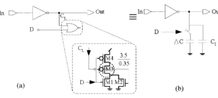
Fig. 2. Proposed DCV with two-input NOR gate. (a) Circuit with digital control. (b) Equivalent circuit with1C capacitance.
in this section. Section III then describes the implementation and experimental results. Conclusions are finally made in Section IV.
II. PROPOSEDDIGITALLYCONTROLLEDOSCILLATOR
A. Digitally Controlled Varactors
Fig. 2(a) illustrates a novel varactor cell using a two-input
NORgate. As described in [7], the gate-to-channel capacitance contributes to total gate capacitance. The proposed method con-trols the capacitance between gate and source or between gate and drain. In Fig. 2(a), theNORgate capacitance at node de-pends on control node ’s value. The total gate capacitance of transistors M2 and M3 varies with input states.
Fig. 2(b) shows the equivalent circuit of Fig. 2(a), an initial capacitance parallels with a capacitance difference . The input controls the capacitance in the output (Out) node. Fig. 3 shows the gate capacitance difference character-istic which is simulated using the HSPICE circuit simulator. The swing-averaged capacitance , as -node is in the 0 state or in the 1 state, is given by
(1) where denotes the simulated gate capacitance shown in Fig. 3. Based on (1), denotes the capacitance
difference between and . Consequently,
the variable delay of the proposed DCV in different states can be calculated easily using the following linear equation:
(2) where denotes the delay factor of driving inverter. The value of the driving inverter is 0.509 (ns/pF) in target 0.35- m 2P4M CMOS cell library. The of Fig. 3 is es-timated to be around 2.8 fF. Therefore, of 1.425 ps
is easily obtained. If NOR gates are attached to the node, the max delay time variation becomes . Moreover, different can be achieved as needed by changing the cell type of the driving inverter (i.e., change the ).
ANANDgate can also be applied to DCV design. Fig. 4 illus-trates three different DCVs: (a) two-inputNANDgate; (b) three-inputNORgate; (c) three-inputNANDgate. For the three-input
NORand three-inputNANDgate, an extra input pin is fixed to 1
Fig. 3. Variation of two-inputNORgate’s capacitance whenD = 0 and D = 1.
Fig. 4. Three different types of DCV cells. (a) Two-input NAND. (b) Three-inputNOR. (c) Three-inputNAND.
TABLE I
COMPARISONSAMONGDIFFERENTTYPES OFPROPOSEDDCV CELLS
and 0, respectively. The marked transistors (M5, M6, M7) pro-duce a large capacitance difference under different states.
Table I lists the comparisons among these DCVs. The three-input NAND/NORgate varactor consumes less power than the 2-inputNAND/NORgate varactor, but it costs more area. Gen-erally, the finer delay resolution can be obtained by decreasing MOS width of (M5, M6, M7).
B. Performance of the Digitally Controlled Varactors
HSPICE circuit simulation is performed for estimating the performance of different type fine-tuning delay cell including the proposed DCV, pass transistor [3], and OAI cell [6] on a standard 0.35- m CMOS 2P4M process. In this simulation, a series of 97 inverters are used in the coarse-tuning stage of the ring oscillator, and the proposed DCV and serves as the fine-tuning delay cell. Totally, 32 DCVs are used in the fine-fine-tuning delay cell . Fig. 5 shows the delay resolution of the fine-tuning stage and the proposed delay cell has finer resolution (about 1.43 ps) than other circuits [3], [6].
Fig. 5. Comparisons among the proposed DCV and other approaches.
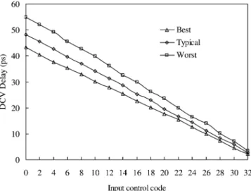
Fig. 6. Proposed DCV using two-inputNORunder different PVT conditions.
The delay cell proposed by [3] has very good linearity but poor resolution and it also has large transistor counts. Oppositely, OAI cell [6] has less transistor counts and less power consumption, but it has nonuniform linearity. Fig. 6 shows the proposed DCV under different process, voltage, temperature (PVT) conditions: (Best: FF, 3.6 V, 0 C), (Typical: TT, 3.3 V, 25 C), and (Worst: SS, 3.0 V, 125 C). The delay resolution of the proposed DCV ranges from 1.28 ps in the best case to 1.61 ps in the worst case. It demonstrates the effectiveness of the proposed DCV to overcome PVT variations.
C. Structure of the Proposed DCO
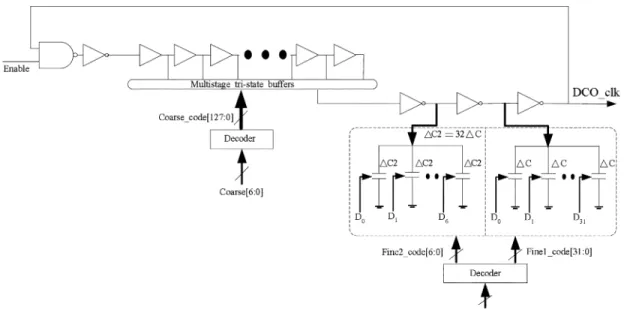
Fig. 7 illustrates the structure of the proposed cell-based DCO
with 15 bits binary weighted control .
The proposed DCO structure is separated into two stages: the coarse-tuning stage and the fine-tuning stage. The higher seven bits of the control code are for coarse-tuning stage, and lower eight bits are for the fine-tuning stage. The coarse-tuning stage uses a 128-to-1 path selector for delay-chain selection. This se-lector is implemented by multistage tristate buffers to reduce
added after the coarse-tuning stage. The fine1 stage consists of 32 DCVs with capacitance difference . 32 identicalNOR
gates with are used to build one DCV. The total capac-itance difference equals to 256 DCVs. The proposedNOR
gate varactors for fine-tuning stage thus can improve delay res-olution by 256 times compared to a simple buffer design.
The period of DCOs output signals equals
(3) where denotes the propagation delay time of coarse buffers, represents the fine-tuning delay time, and is the constant factor for delay time because of one extraNANDgate, a multistage tri-state buffer and the intrinsic
delay caused by capacitance of fine-tuning cells in the DCO ring. Equation (3) can be rewritten as follows:
(4) where denotes the number of selected coarse buffers. and represent the number of turned on DCVs in fine1 and fine2 stages, respectively. Meanwhile, and are vari-able delay which can be calculated from (2). Therefore, (4) pro-vides an easy method of calculating the timing period of DCO output.
III. IMPLEMENTATION ANDEXPERIMENTALRESULTS
A. Implementation Overview
The proposed DCO with novel DCVs is applied to all-dig-ital PLL (ADPLL) design. The test chip is fabricated using a standard 0.35- m 2P4M CMOS process. The designed DCO consists of two major functional blocks as illustrated in Fig. 7, namely the ring structure and decoder. Moreover, the decoder part is described by Verilog-HDL. The ring structure with DCVs is described at the gate level. A Verilog-HDL model of DCVs is first built from HSPICE simulation results for co-simulation with other digital blocks. Next, source codes are synthesized to gate-level netlists and schematics for further simulation and verifications. Once the functions have been correctly verified, an automatic placement and routing (APR) tool is used to com-plete the physical layout.
In APR process, the designed DCO must be grouped in a restricted region to minimize the induced capacitance and the ring structure of DCO had to be placed regularly rather than randomly. Furthermore, the post-layout simulation is performed to ensure the monotonic response of DCO and timing resolution. The APR process will be refined until the target specification is achieved.
Fig. 7. Proposed digitally controlled oscillator with DCV in the fine-tuning stage.
Fig. 8. Microphotograph of DCO test chip.
B. Laboratory Test Result
Fig. 8 is a microphotograph of the ADPLL. The proposed DCO is located in the upper left corner of the test chip and occupies 0.04 mm of chip area (i.e., 200 m 200 m). This DCO has been measured for different settings. Initially, the DCO output frequency is directly measured using LeCory LC584A at 3.3 V/25 C, and the measured results demonstrate that the operating frequency of the DCO ranges from 18 to 214 MHz (i.e., 55.555 ns to 4.673 ns). Moreover, the average step resolution is 1.55 ps. In Fig. 9, the measured results are compared to linear delay (4). Fig. 9 also reveals that linear delay (4) can be used to estimate DCO timing period.
Table II lists the chip measurement results compared with conventional approaches [3], [5], [6]. The proposed DCO with 15 bits control codes achieves the finest LSB resolution and best
Fig. 9. Chip measured results compared to linear (4) under 3.3 V/25 C.
TABLE II
COMPARISONWITHEXISTINGDCOS
portability. Additionally, the proposed DCO also consumes less power as compared with [5] and [6].
IV. CONCLUSION
A portable digitally controlled oscillator using two-inputNOR
gates as digitally controlled varctors has been presented. Dif-ferent configurations based onNOR/NANDgates have also been
first-time silicon success.
ACKNOWLEDGMENT
The authors are grateful to the reviewers for their constructive comments to improve the manuscript. The authors would also like to thank the members of SI2 Laboratory of National Chiao Tung University, Taiwan, R.O.C., for many fruitful suggestions in implementation.
technology node for reduced design and process sensitivities,” in Proc. ISQED’02, Mar. 2002, pp. 148–153.
[4] T. Olsson and P. Nilsson, “Portable digital clock generator for digital signal processing applications,” Electron. Lett., vol. 39, pp. 1372–1374, Sep. 2003.
[5] E. Roth, M. Thalmann, N. Felber, and W. Fichtner, “A delay-line based DCO for multimedia applications using digital standard cells only,” in Dig. Tech. Papers ISSCC’03, Feb. 2003, pp. 432–433.
[6] C.-C. Chung and C.-Y. Lee, “An all digital phase-locked loop for high-speed clock generation,” IEEE J. Solid-State Circuits, vol. 38, no. 2, pp. 347–351, Feb. 2003.
[7] J. M. Rabaey, Digital Integrated Circuits—A Design Perspectives. En-glewood Cliffs, NJ: Prentice-Hall, 1996.