The effects of growth temperature on the microstructure and
Ž
.
electrical barrier height in PtSi
rp-Si 100 Schottky barrier
detector
Gwo-Ji Horng
a,U, Chun-Yen Chang
a, Chia Ho
b, Ching-Yuan Lee
b, T.Y. Huang
aa
Department of Electronics Engineering and Institute of Electronics, National Chiao Tung Uni¨ersity, Hsinchu, Taiwan, ROC
b
Microelectronic De¨ices Laboratory, CSIST, P.O. Box 90008-16-21, Lungtan, Taoyuan, Taiwan, ROC Received 13 December 1999; received in revised form 26 May 2000; accepted 9 June 2000
Abstract
The effects of growth temperature on the microstructure and electrical barrier height of the PtSi Schottky barrier detector ŽSBD have been investigated. PtSi films, 4 nm in thickness were deposited at various temperatures ranging from 350 to 550. ⬚C.
Ž . Ž .
The electron diffraction patterns showed that PtSi film formed at 350⬚C depicts an intermingling of both 110 and 121 Ž .
orientations. However, only 121 orientation was shown when the PtSi films were formed above 450⬚C. Moreover, SBD formed at 350⬚C was found to depict an electrical barrier that is approximately 0.02 eV higher than those formed above 450⬚C. Although the microstructure and the electrical barrier height of the PtSi film do not change when the formation temperature was further increased from 450 to 550⬚C. Nevertheless, the higher formation temperature resulted in a larger grain size, indicating that grain size alone does not affect the barrier height of the resultant SBD.䊚 2000 Elsevier Science S.A. All rights reserved.
Keywords: PtSi; Schottky barrier; Transmisson electron microscopy; Electron diffraction
1. Introduction
Ž .
The PtSi Schottky barrier detector SBD has been applied to radiation detection in the mid infrared range. Due to its process compatibility with standard
silicon-Ž .
based very large scale integrated circuit VLSI tech-nologies, large two-dimensional PtSi arrays can be
inte-Ž .
grated with the charge coupled device CCD
multi-w x
plexer circuits on the same silicon substrate 1᎐4 . The diodes used for sensing in these arrays are normally
Ž .
fabricated using p-Si 100 substrate and depict excel-lent signal-to-noise performance in the 3᎐5 m detec-tion window. A systematic study about the epitaxial
Ž .
orientation of PtSi grown on Si 100 substrate at
dif-UCorresponding author. Tel.:q886-3-445-3836; fax:
q886-3-471-3782.
Ž .
E-mail address: [email protected] G. Horng .
ferent formation temperatures was reported by Konuma w x
and Utsumi 5 . They found that the epitaxial orienta-tion depends critically on the substrate temperature. Two orientations were found and ascribed to two
dif-w x
ferent formation mechanisms 6 . Specifically, Pt Si was2 formed when Pt was evaporated onto Si substrate that was held at 320⬚C, and transformed into PtSi phase
Ž .
with the 110 orientation during subsequent sintering. On the other hand, PtSi film was directly formed along
Ž .
the 121 plane when the Pt evaporation was performed with the substrate held at 400⬚C, and underwent no further change during subsequent heat treatment. Fi-nally, the effects of Si substrate orientation on the PtSi
w x Schottky barrier height have also been studied 7 . The optical Schottky barrier height was found to be 0.216
Ž . Ž .
eV for PtSirp-Si 100 and 0.292 eV for PtSirp-Si 111 , respectively. It was believed that the difference in atomic arrangements at the interface accounts for the
0040-6090r00r$ - see front matter 䊚 2000 Elsevier Science S.A. All rights reserved. Ž .
observed 0.076 eV difference in the optical Schottky barrier height. However, the conventional optical mea-surements used to extract the Schottky barrier height of a PtSirp-Si were known to be strongly dependent on w x the measurement system and diode leakage current 8 . To alleviate these shortcomings, I᎐V characteristics at different temperatures have been recently proposed for w x extracting the barrier height with better accuracy 9 . The main advantage of the so-called ‘I᎐V-T technique’ is that the inaccuracy associated with leakage current can be effectively eliminated.
In this paper, we report the dependence of the growth conditions of the PtSi film on the microstruc-ture and the electrical Schottky barrier height. High
Ž .
resolution transmission electron microscopy HRTEM and electron diffraction were applied to characterize the microstructure of the PtSi films with different growth conditions. The Schottky barrier heights for each formation condition were determined by I᎐V-T current-voltage measurements at a reverse bias voltage of 4 V. Our results show that PtSi films grown at
Ž .
temperatures higher than 450⬚C depict only 121 ori-entation and a lower electrical barrier height. In addi-tion, the film grain size does not seem to affect the electrical barrier height with a given film orientation.
2. Experimental details
The cross-sectional diagram of the PtSi SBD struc-ture is shown in Fig. 1. In order to reduce the leakage current of the PtSi SBD, an nq guard ring was imple-mented on the periphery of the PtSi film. The substrate
Ž .
used was p-type Si 100 with a resistivity of 25᎐30 ⍀cm. Thin Pt films were deposited on Si substrate, using an electron gun evaporator in an ultra high
Ž .
vacuum UHV chamber. The base pressure of the chamber was 2=10y10 mbar. The thickness of the deposited Pt film was monitored in situ by a micro-bal-ancer quartz crystal. The substrate temperature during the Pt deposition was varied between 350 and 550⬚C. Immediately after the Pt deposition, an in situ anneal-ing at the same temperature was performed to form PtSi through solid-state reaction between Pt and Si. Detailed growth conditions are summarized in Table 1. Three different formation conditions were applied in this study to obtain PtSi films with different microstruc-tures. The film thickness and its uniformity were ex-amined using high resolution cross-sectional TEM ŽHRTEM . The dark-field plain-views of TEM were. used to analyze the characteristics of the PtSi grains. The phase and the orientation of the film were de-termined from the electron diffraction patterns. In order to correlate the electrical characteristics with the
Fig. 1. Cross-sectional diagram for the PtSi Schottky barrier detec-tor.
film quality, the I᎐V-T current᎐voltage measurements at a reverse bias of 4 V were carried out at tempera-tures ranging from 80 to 150⬚K. The operating temper-ature of the detector was monitored by the Si diode directly attached on the detector carrier. The Schottky barrier heights were determined by extracting from the slopes of the Richardson plot at 4 V reverse bias.
3. Results and discussion
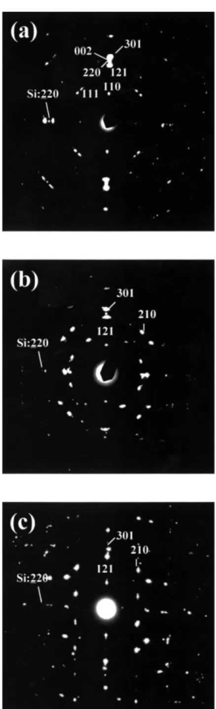
Fig. 2 shows the cross-sectional pictures of HRTEM for different formation conditions. The film thickness is approximately 4 nm for all the formation conditions. From the plain view pictures of the PtSi films analyzed by HRTEM, as shown in Fig. 3, the PtSi grains are quite different for different formation temperatures. In particular, PtSi grains with small random round-shape and relatively disoriented are observed at 350⬚C forma-tion, as shown in Fig. 3a. The round-shape grains seem to turn into small rectangular shapes and become more oriented when the formation temperature is increased to 450⬚C, as shown in Fig. 3b. While for 550⬚C forma-tion, the film depicts grains that are similar but much larger in size to those of the 450⬚C formation, as shown in Fig. 3c. The parallel Moire fringe spacing observed is
´
˚
approximately 19 A. This value is very close to the
Ž .
fringe spacing caused by the interference of 220 Si
Ž . Ž .
reflection across the PtSi 301 and Si 110 planes,
Ž .
indicating PtSi film with 121 orientation. Fig. 4 illus-trates the e-beam diffraction patterns for these films. All of these diffraction patterns show scattered spots, indicating that the PtSi films are epitaxially grown on Si
Table 1
The formation conditions of PtSi Schottky barrier detectors Conditions Temperature for In situ annealing
Ž .
Type Pt deposition Tsub for PtSi formation
A 350⬚C 350⬚Cr30 min
B 450⬚C 450⬚Cr20 min
Ž100 substrate. The diffraction pattern of PtSi film.
Ž .
formed at 350⬚C shows an intermingling of both 110
Ž .
and 121 orientations, as illustrated in Fig. 4a. This result is consistent with the observation by Ghozlene et
w x
al. 6 . However, for the PtSi film formed at 450 and 550⬚C, the electron diffraction patterns reveal that the
Ž .
film only depicts 121 orientation, as illustrated in Fig. 4b,c. The only difference between the two films formed at 450 and 550⬚C is that the diffraction pattern is more repeatable for the film formed at 550⬚C, indicating that the film formed at 550⬚C is more crystalline than that formed at 450⬚C. This observation is consistent with the result from the plain-view HRTEM that the grain size formed at 550⬚C is much larger than that formed at 450⬚C. Nevertheless, the X-ray diffraction provides a better method to determine the crystalline of the film quality. However, the diffraction signal is quite small
Ž .
due to the relatively thin PtSi layer i.e. 4 nm .
The current density of the Schottky diode as a func-tion of applied voltage can be expressed as follows:
w Ž . x
IsA J exp qVrnkT y1e s and
U 2 Ž .
JssA T exp yqrkT
Fig. 2. High resolution cross-sectional view of TEM for PtSi films Ž .
formed at different growth conditions. a Tsu bs350⬚C; annealing:
Ž . Ž .
350⬚C, 30 min; b T s450⬚C, annealing: 450⬚C, 20 min; c T ssub sub
550⬚C, annealing: 550⬚C, 10 min. The film thickness is 4 nm for all growth conditions.
Ž . Fig. 3. Plain views of poly grains formed at different conditions. a
Ž .
Tsubs350⬚C, annealing: 350⬚C, 30 min; b T s450⬚C, annealing:sub
Ž .
450⬚C, 20 min; c T s550⬚C, annealing: 550⬚C, 10 min.su b
where J is the saturation current density, n is thes ideality factor, AU is the effective Richardson constant, T is the device operation temperature, A is the detec-e tor area, and is the barrier height of the Schottky diode. The saturation current of the PtSirp-Si Schottky diode can be obtained from the reverse-biased I᎐V characteristics. The electrical barrier height can be extracted from the slope of the so-called Richardson plot. Fig. 5 is the resultant Richardson plot of PtSirp-Si SBDs operated under 4 V reverse bias for each forma-tion condiforma-tion. The electrical barrier height with bar-rier height lowering effect is extracted from the slope for each line. It is found that while both the 450 and 550⬚C formations depict essentially identical character-istics in the Richardson plot, the extracted barrier height of 350⬚C formation is approximately 0.221 eV, which is approximately 0.02 eV higher than that of 450 and 550⬚C formations. One plausible explanation for the barrier height difference between 350⬚C and other formation conditions is due to the different poly phase orientation of the PtSi films. As described earlier, the
Ž .
PtSi film depicts an intermingling of both 110 and Ž121 orientations with small random shape and rela-.
tively disorientation for the 350⬚C formation. While
Ž .
more orientated PtSi films with 121 orientation are obtained for both 450 and 550⬚C formations. It thus
Ž .
appears to be likely that the 121 orientated PtSi films have a larger metal work function than that of the film
Ž .
with 110 orientation. As a result, the electrical
Schot-Ž .
tky barrier height of PtSirp-Si 100 is reduced for the
Ž .
PtSi film with 121 orientation. While for the PtSi films with the same orientation, no noticeable difference is observed on the barrier height, even though the grain
Fig. 4. Electron diffraction patterns of poly grains formed at
differ-Ž . Ž .
ent conditions. a Tsu bs350⬚C, annealing: 350⬚C, 30 min; b T ssub Ž .
450⬚C, annealing: 450⬚C, 20 min; c T s550⬚C, annealing: 550⬚C,sub 10 min.
Fig. 5. Richardson plots of PtSirp-Si SBDs operated under 4 V reverse bias for different formation conditions.
size could be quite different. This explains why the electrical barrier heights of the PtSi films formed at 450 and 550⬚C are essentially identical, despite the big difference in their grain size.
4. Conclusions
The effects of the PtSi film growth conditions on the microstructure and the electrical barrier height were analyzed in detail through the high-resolution TEM, e-beam diffraction pattern, and I᎐V-T technique. Our results show that PtSi film grown at 350⬚C depicts an
Ž . Ž .
intermingling of 110 and 121 orientations, while PtSi films show identical orientations and grain shape with
Ž .
only 121 orientation for both 450 and 550⬚C forma-tions, albeit the grain size is much larger for 550⬚C formation. I᎐V-T measurements also show that while PtSi films grown at 450 and 550⬚C depict essentially the same electrical barrier height, the film grown at a lower 350⬚C depicts a higher electrical barrier height. Since the two films at 450 and 550⬚C formations depict essen-tially the same electrical barrier height, it clearly indi-cates that the grain size alone does not play any major role in determining the barrier height.
References
w x1 W.F. Kosonocky, in: E.L. Dereniak, R.E. Sampson Eds. , In-Ž . frared Detectors and Focal Plane Arrays, Orlando, USA, April
Ž . 18᎐19, 1990, SPIE proceedings 1308 1990 2.
w x2 T.S. Villani, W.F. Kosonocky, in: E.L. Dereniak, R.E. Sampson ŽEds. , Infrared Detectors and Focal Plane Arrays, Orlando,.
Ž . USA, March 30᎐31, 1989, SPIE proceedings 1107 1989 9. w x3 D.L. Clark, J.R. Berry, in: B.F. Andresen, M. Scholl, I.J. Spiro
ŽEds. , Infrared Technology XVII, San Diego, USA, July 22. ᎐26, Ž .
1991, SPIE Proceedings, 1540 1991 303.
w x4 N. Yutani, H. Yagi, M. Kimata, J. Nakanishi, S. Nagayoshi, N. Ž .
Tsubouchi, in: E. Fossum, J. Bosiers Eds. , Detectors, Sensors and Displaysᎏ Charge Coupled Devices and MSM
Photode-tector, Washington DC, USA, December 8᎐11, 1991, Interna-tional Electron Devices Meeting, 1991, p. 175.
w x5 K. Konuma, H. Utsumi, J. Appl. Phys. 76 1994 2181.Ž . w x6 H.B. Ghozlene, P. Beaufrere, A. Authier, J. Appl. Phys. 49´
Ž1978 3998..
w x7 P.W. Pellegrini, C.E. Ludington, M.M. Weeks, J. Appl. Phys. 67 Ž1990 1417..
w x8 W.F. Kosonocky, F.V. Shallcross, T.S. Villani, J.V. Groppe, IEEE Tran. Electron Devices ED-32, 1985, p. 1564.
w x9 P.G. McCafferty, A. Sellai, P. Dawson, H. Elabd, Solid-State Ž .