Field emission properties of CNT
–ZnO composite materials
Chien-Sheng Huang
a,⁎
, Chun-Yu Yeh
a, Yung-Huang Chang
b, Yi-Min Hsieh
a, Chien-Yeh Ku
a, Quan-Ting Lai
aa
Graduate school of Optoelectronics, National Yunlin University of Science and Technology, Douliou 64002, Taiwan
b
Department of Materials Science and Engineering, National Chiao Tung University, Hsinchu 30050, Taiwan
a b s t r a c t
a r t i c l e i n f o
Available online 12 November 2008 Keywords:
CNT–ZnO Composite materials Field emission properties
CNT–ZnO composite materials were successfully grown by thermal chemical vapor deposition (thermal CVD). First, Multiwalled Carbon nanotubes were synthesized in the temperature range of 500–700 °C. After coating Au nanoparticles on such grown CNTs, ZnO nanowires were synthesized via Zn evaporation method at 500 °C. SEM images showed that these CNT–ZnO composites were spinous, and XRD analyses showed that the spinal ZnO were crystalline. The turn-onfield of CNT–ZnO composite materials with 500 °C growth temperature of underlying CNTs was 3.72 V/μm, which was 5.58 V/μm for CNTs grown at 500 °C. It was also found that the higher temperature (<550 °C) the underlying CNTs were grown at, the betterfield emission properties CNT–ZnO composite materials have. The ID/IGratio from Raman spectroscopy of CNTs decreased as the growth temperature of CNTs increased. The graphitization of underlying CNTs played an important role in the Field emission of CNT–ZnO composite materials.
© 2008 Elsevier B.V. All rights reserved.
1. Introduction
One-dimensional (1D) nanostructural materials have attracted considerable attention due to their unique fundamental physical properties and potential high-technology applications in the fabrica-tion of nanoscale devices [1]. The nanotubes and nanowires are promising candidates of idealfield emission electron sources because of their high aspect ratio geometry and small tip radius of curvature. Since the discovery of carbon nanotubes (CNTs) in 1991[2], they have been the most promising material due to their unique structure and properties. ZnO, as an oxide, presents many remarkable characteristics due to its high mechanical strength, good optical quality, chemical stability and excellent piezoelectric properties[3]. In the past, many studies have investigated thefield emission properties of CNTs[4–6]
and ZnO nanostructures[7–10].
In this study, a CNT–ZnO composite was synthesized and exhibited different field emission properties from general CNTs or ZnO nanowires.
2. Experimental details
The growth of CNTs was carried out by using the thermal chemical vapor deposition (thermal CVD) system at temperatures of 500 °C, 550 °C, 600 °C, 650 °C, and 700 °C. Prior to the growth, an Fe layer was deposited as catalysts on a (100) p-type silicon
substrate by the RF sputtering with Ar plasma. During the growth, the N2gas wasfirst introduced into reaction tube at a flow rate of 100 sccm with 8.67 × 10² Pa for 30 min. Reaching the growth temperature, N2was switched off and C2H2was switched on at a flow rate of 30 sccm with 4.67×10² Pa for 20 min, and then swiched off. Finally, the reaction tube was cooled down at the N2 ambient.
Such grown CNTs was then coated Au as the catalyst to synthesize ZnO. By heating pure zinc powder at the temperature 500 °C in a horizontal tube furnace and using Argon and oxygen gases as a carrier and a reaction gas during the fabrication process, spinal ZnO was formed on the underlying carbon nanotubes.
The morphology and crystal structure properties of the samples were examined byfield emission scanning electron microscopy (FE-SEM), Raman spectroscopy, and X-ray diffractometer (XRD), respec-tively. Field emission measurements were carried out by using a diode configuration in a vacuum chamber, which was pumped down to 2.67 × 10− 4 Pa, and using a Keithley 237 source meter as an analyzer. The turn-on electric fields of tested materials were calculated from the values of voltage Vto divided by the average gap between the material surface and the anode. Vto was measured when thefield emission current reached 1.0 μA, and the uncertainty was ± 1 V. The gap was measured by a step gauge, and the uncertainty was ± 1μm.
3. Results and discussion
Fig. 1 showed the SEM image of underlying CNTs at growth temperatures range of 500–700 °C. It was found that the higher
⁎ Corresponding author.
E-mail address:[email protected](C.-S. Huang).
0925-9635/$– see front matter © 2008 Elsevier B.V. All rights reserved. doi:10.1016/j.diamond.2008.10.058
Contents lists available atScienceDirect
Diamond & Related Materials
temperature the CNTs were grown at, the height of CNTs increased from 0.58 to 3.33μm.
Fig. 2showed the Raman spectra (taken with the 532 nm Nd: YAG laser) of underlying CNTs at the growth temperature range of 500–700 °C. Both the typical D band (~1350 cm− 1) and G band (~ 1580 cm− 1) for multi-walled CNTs appeared[11]. The Lorentzian componentsfitting gave the peak values and the ratio ID/IG, which would be a graphitization index for CNTs. It was found that the higher temperature the CNTs were grown at, the ID/IG ratio of CNTs decreased from 1.165 to 0.800. As stated in the literatures
[12–14], CNTs grown at higher temperatures would have smaller ID/IGratio and therefore higher graphitic crystallinity.
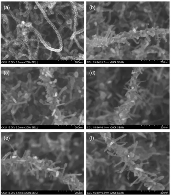
Fig. 3(a) showed the SEM image of Au nanoparticles on the underlying CNTs. Au nanoparticles have the diameter of ~5 nm.
Fig. 3(b)–(f) showed SEM images of the CNT–ZnO composite with the underlying CNTs of different growth temperatures. The XRD pattern of CNT–ZnO composite was shown inFig. 4. All diffraction peaks matched the wurtzite ZnO structure with the lattice constants of a = 0.325 nm and c = 0.52 nm (JCPDS No. 36-1451). The peaks at
which 2θ equals 31.7°, 34.4°, 36.3°, 47.5°, and 56.6° represent ZnO (100), (002), (101), (102), and (110) reflections, respectively.
Thefield emission (FE) properties were characterized by using a Keithley 237 source meter as an analyzer. The FE current–voltage characteristics were further analyzed by a simplified Fowler–Nord-heim (F–N) equation: J =Aβ 2E2 ϕ exp −Bϕ 3=2 βE ! ð1Þ where J is the emission current density, E is the macroscopicfield, ϕ is the work function of the emitter, A and B are the F–N constants with values of 1.56 × 10− 10A eVV− 2and 6.83 × 10³eV− 3/2Vμm− 1, respectively
[15]. Theβ is the FE enhancement factor that represents the true value of the electricfield at the tip compared to its average macroscopic value. Theβ can be calculated from the slope of the FN plot [ln(J/E2) versus 1/E plot] if the work function is known.
Fig. 5(a) and (b) showed the emission current density of the underlying CNTs with different growth temperatures versus electric
Fig. 1. SEM images of underlying CNTs at different growth temperatures: (a) 500 °C, (b) 550 °C, (c) 600 °C, (d) 650 °C, (e) 700 °C; and (f) the height of underlying CNTs versus growth temperatures.
Fig. 2. Raman spectra of underlying CNTs at different growth temperatures: (a) 500 °C, (b) 550 °C, (c) 600 °C, (d) 650 °C, (e) 700 °C.
Fig. 3. SEM images of (a) Au nanoparticles on underlying CNTs and CNT–ZnO composite materials with different growth temperature of underlying CNTs: (b) 500 °C, (c) 550 °C, (d) 600 °C, (e) 650 °C, (f) 700 °C.
Fig. 4. XRD pattern of CNT–ZnO composite materials with different growth temperature of underlying CNTs.
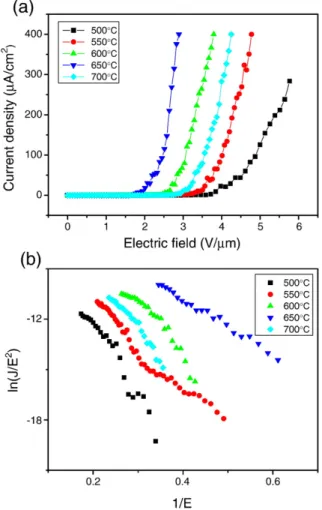
field, and the corresponding F–N plot, respectively. The work function of CNTs was assumed to be 5 eV[16]. As the growth temperature of underlying CNTs increased from 500, 550, 600 to 650 °C, the turn-on field was decreased from 5.58, 3.50, 1.84 to 1.45 V/μm and the β was increased from 1167, 2077, 3604 to 6032, respectively. By comparison with the Raman spectroscopy in theFig. 2, the tendency was obvious that the underlying CNTs grown at higher temperatures (≥650 °C) would have higher graphitic crystallinity, lowerfield emission turn-on field and larger β. This was also stated in the literature that the emission current of CNTs increased with the graphitic crystallinity and the growth temperature of CNTs[17]. However, CNTs grown at 700 °C had the turn-onfield of 2.25 V/μm and the β of 3075, not better than that of which grown at 600 °C. Since thefield emission properties of CNTs mat were dependant not only on the single nanotube, but also the field-screening effect caused by the proximity of neighboring nanotubes[18], such emission property degradation of CNTs grown at 700 °C could be explained.
As stated in the literature[19], when the height of CNTs was deucedly high, thefield-emission characteristic was poor, which was likely to be due to the screening effect. As the underlying CNTs grown at higher temperatures (≥600 °C), the heights were order of micro-meter magnitude. The reason was that the CNT–ZnO compo-sites with higher temperatures CNTs (≥600 °C) were affected by field-screening effect. Because the height of CNTs at 700 °C was extremely greater than that others, its field-screening effect was especially enormous, and degraded the turn-on field and the FE enhancement factorβ.
The general ZnO nanowires were synthesized on silicon (100) substrates with Au catalysts by heating pure zinc powder at
fields were 3.72, 2.68, 2.40, 1.64 and 2.68 V/μm, respectively. And the β's were 2082, 2442, 2576, 4490 and 2426, respectively. All the CNT–ZnO composite materials have better field emission ability than that of general ZnO nanowires. However, by comparison with CNTs mat, thefield emission properties of CNT–ZnO composites could be categorized as two groups: one is with lower turn-on voltage and higherβ than that of corresponding CNTs mat grown at the same temperature (500 °C, 550 °C), and the other is with higher turn-on voltage and lowerβ than that of corresponding CNTs mat grown at the same temperature (600 °C, 650 °C, 700 °C). From
Fig. 1(f), the height of underlying CNTs of the former group was about hundreds of nano-meter magnitude, and the one of the latter group was above the order of micro-meter magnitude. As mentioned, the
Fig. 5. (a) Emission current density versus electricfield, and (b) the corresponding F–N plot of the underlying CNTs with different growth temperature.
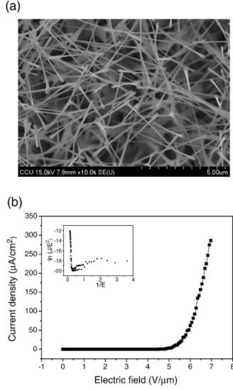
Fig. 6. (a) SEM images, and (b) Emission current density versus electricfield of ZnO nanowires with diameters of 80–100 nm.
screening effect was important when the height of CNTs were deucedly high. Thefield emission experiments of CNT–ZnO compo-sites showed that micro meter seemed to be a criterion scale. Hence thefield emission properties of CNT–ZnO composites, which had the underlying CNTs grown at 500 and 550 °C, were better than that of general CNTs grown at the same temperature. The reason was that the spinal ZnO on the surface of CNT–ZnO composite played as a sharp emission center.
4. Conclusions
The field-emission characteristics of CNT–ZnO composite were different from that of general CNTs or ZnO nanotubes, and the temperature at which the underlying CNTs were grown exhibited great effects on it. The turn-onfield of CNT–ZnO composite materials with 500 °C and 550 °C growth temperature of underlying CNTs were 3.72 and 2.68 V/μm, which were 5.58 and 3.50 V/μm for CNTs grown at 500 °C and 550 °C, respectively. The spinal ZnO on the surface of CNT– ZnO composites played as a sharp emission center and gave rise to the increasing of β factor. However, the screening effect should be considered when the height of CNTs increased to a few micro-meter scale ranges.
Fig. 7. (a) Emission current density versus electricfield, and (b) the corresponding F–N plot of CNT–ZnO composite materials with different growth temperature of underlying CNTs.
References
[1] Y. Xia, P. Yang, Y. Sun, Y. Wu, B. Mayers, B. Gates, Y. Yin, F. Kim, H. Yan, Adv. Mater. (Weinheim, Ger.) 15 (2003) 353.
[2] S. Iijima, Nature 354 (1991) 56.
[3] S.J. Pearton, D.P. Norton, K. Ip, Y.W. Heo, T. Steiner, Superlattice Microstruct. 34 (2003) 3.
[4] W.A. de Heer, A. Chatelain, D. Ugarte, Science 270 (1995) 1179.
[5] S.C. Tseng, C.H. Li, Y.Y. Lin, Ching Hsiang Tsai, Z.P. Wang, K.C. Leou, C.H. Tsai, S.P. Chen, J.Y. Lee, B.C. Yao, Diamond Relat. Mater. 14 (2005) 2064.
[6] Y.M. Wong, W.P. Kang, J.L. Davidson, B.K. Choi, W. Hofmeister, J.H. Huang, Diamond Relat. Mater. 14 (2005) 2069.
[7] W.I. Park, D.H. Kim, S.-W. Jung, G.-C. Yi, Appl. Phys. Lett. 80 (2002) 4232. [8] C.J. Lee, T.J. Lee, S.C. Lyu, Y. Zhang, H. Ruh, H.J. Lee, Appl. Phys. Lett. 81 (2002) 3648. [9] M.H. Huang, S. Mao, H. Feich, H. Yan, Y. Wu, H. Kind, E. Weber, R. Russo, P. Yang,
Science 292 (2001) 1897.
[10] C.X. Xu, X.W. Sun, B.J. Chen, Appl. Phys. Lett. 84 (2004) 1540.
[11] M.S. Dresselhaus, G. Dresselhaus, P.H. Avouris, Carbon Nanotubes: Synthesis, Properties and Applications, Springer Series in Topics in Applied Physics, vol. 80, Springer-Verlag, Berlin, 2001.
[12] P.H. Tan, S.L. Zhang, K.T. Yue, F.M. Huang, Z.J. Shi, X.H. Zhou, Z.N. Gu, J. Raman Spectrosc. 28 (5) (1997) 369.
[13] C.F. Chen, C.L. Tsai, C.L. Lin, Diamond Relat. Mater. 12 (2003) 1500.
[14] L. Valentini, I. Armentano, J.M. Kenny, L. Lozzi, S. Santucci, Diamond Relat. Mater. 12 (2003) 821.
[15] R.H. Fowler, L. Nordheim, Proc. R. Soc. London, Ser. A 119 (1928) 173.
[16] J.M. Bonard, J.P. Salvetat, T. Stockli, L. Forro, A. Chatelain, Appl. Phys. A: Mater. Sci. Process. 69 (1999) 245.
[17] L. Wang, Z. Sun, T. Chen, W. Que, Solid-State Electron. 50 (2006) 800.
[18] L. Nilsson, O. Groening, C. Emmenegger, O. Kuettel, E. Schaller, L. Schlapbach, H. Kind, J-M. Bonard, K. Kern, Appl. Phys. Lett. 76 (2000) 2071.
[19] S. Fujii, S. Honda, H. Kawai, K. Ishida, K. Oura, M. Katayama, Diamond Relat. Mater. 17 (2008) 556.
[20] C.J. Lee, T.J. Lee, S.C. Lyu, Y. Zhang, H. Ruh, H.J. Lee, Appl. Phys. Lett. 81 (2002) 3648. [21] J.M. Green, L. Dong, T. Gutu, J. Jiao, J.F. Conley Jr., Y. Ono, J. Appl. Phys. 99 (2006)