國 立 交 通 大 學
材料科學與工程學系
博 士 論 文
鎳鐵圖形化微結構中
自旋傳輸及磁化翻轉行為之研究
Study on Spin Transport and Magnetic Reversal
Behavior in Patterned NiFe Structure
研 究 生:陳東呈
指導教授:姚永德 博士
韋光華 博士
中文摘要
本論文的研究以電子束微影及舉離技術,製作次微米級和奈米級的圖形化磁 性薄膜樣品。並藉由磁力顯微儀的量化分析及磁阻量測,來研究該圖形化磁性薄 膜的磁化翻轉以及自旋傳輸的現象,商業化的磁性穿隧界面元件也在溫度變化的 條件下量測其穿隧磁阻的變化。 在一個由兩段不同線寬所組成的磁性長線中,磁力顯微儀的分析結果顯示, 不同區域的磁化翻轉現象能被各別地分開並互相比較。寬度越寬的線段,其端點 雜散磁力越強;相反地,越細的線段其端點的矯頑場越強,這導因於形狀異向性 的效應,也因此在頸部(粗細線段交接處)的矯頑場易受影響,此影響來自於兩線 段的磁化彼此相向時的競爭,在頸部處兩同極性磁極的互斥結果使得此處的矯頑 場變弱。在磁性穿隧界面元件的熱效應研究中,磁阻變化率在 140℃時,降到約 為在室溫的 87%。這意味著該元件在一般使用狀況中能適應儀器或電器所產生略 高於室溫的溫度(60–80 ℃),而數據顯示在該溫度此元件之磁阻變化率仍能保有 在室溫的 90-95%。我們也製作了三層的環形自旋閥及單層的磁性環並量測其磁 阻,在單層環中,由電流所驅動的磁區壁移動,其所需的臨界電流密度約 1.5 ~ 3.5 × 10⁷ A/cm2;在三層環形自旋閥的磁化翻轉過程中,所研究的元件尺寸極可能落 在渦旋態和洋蔥態臨界的邊界上。因為觀察到的數據顯示某一暫穩態隨機地出 現,該暫穩態是軟磁層處於渦旋態,而硬磁層處於洋蔥態。由於單層及三層的量 測方式皆無法提供明確辨認渦旋方向的方法,故我們接著製作橫向的自旋閥,並 利用其非局域的量測方式來判斷渦旋態的旋向。此非局域的橫向自旋閥直接探測 銅導線中,來自鐵磁環因自旋注入所產生的自旋堆積訊號,也因此能得知鐵磁環 的旋向。經由數據推算,該橫向自旋閥在銅質擴散通道裡的自旋級化率約為 2%。 而在橫向自旋閥的另一種量測中,局域的量測方式產生一個反對稱於零磁場的訊 號,幾乎是等同於一般磁滯曲線的訊號。該訊號顯然來自於磁性跟非磁性交接介II
面的電阻訊號。在一系列有系統的尺寸變化研究下,數據結果顯示該訊號來自於 磁性跟非磁性交接介面的異常霍爾效應。
ABSTRACT
Submicron- and nano-sized magnetic patterns were fabricated by e-beam lithography with lift-off techniques. The magnetoresistance (MR) measurements and quantitative analysis of magnetic force microscopy (MFM) were using to investigate the spin transports and magnetic reversal behaviors of these magnetic patterns. The commercial magnetic tunnel junctions (MTJs) were also measured at various temperatures to observe its thermal effects.
The MFM were used to investigate a permalloy (Py) strip including two parts with different widths. The results indicated that the magnetic behaviors in different sections of the strip can be separated. The intensity of the phase-shift in the wider end is stronger than that in the narrower one. In contrast, the coercive force in the narrower end (9 Oe) is larger than that in the wider one (8 Oe). This is due to a strong anisotropic effect, and thus the Hc in the neck section could be strongly affected by the competition of the head-to-tail magnetic configurations in the two parts of the strip wire. This results in a small Hc in the neck section.
For the thermal effect measurement of the MTJs, the MR ratio at 140 ℃ remained roughly 87% of that at room temperature. The operational temperature of electronic equipments is generally around 60–80 ℃ and the MR ratio of the MTJs at such temperatures be preserved in a considerable portion (90–95%) of that at room temperature.
Single-layered and tri-layered spin valve rings were investigated by MR measurements. The critical current density of current-induced domain wall motion in the single-layered Py ring is about 1.5 ~ 3.5 × 10⁷ A/cm2. With the present size, the tri-layered spin valve was possibly in the critical boundary between the formations of vortex and onion. Within this state, the soft ring was in vortex state and the hard one
IV
was in the forward onion state.
The nonlocal lateral spin valve (NLSV) devices were also constructed to detect the vortex chirality of the ring. The spin polarization induced in Cu diffusive channel of the NLSV devices in the present work was estimated at about 2%. The spin signals were also enhanced by shortening the distance of the diffusive channel.
Finally, we investigated the Cu-Py cross structure through which charge current flows and the resistance of the contact region. The concept of this structure was from the NLSV studies mentioned above. When choosing one voltage electrode as the spin injector itself, the probe arrangement was no longer the nonlocal geometry, and hence the signal from the local contact region was sensed. This signal exhibited a magnetic hysteretic loop, i.e., odd-asymmetric roughly equals to the zero field. We found the variation of the odd-asymmetric signals directly related to the switching of the spin injector at the contact region (the Cu-Py cross). It was attributed to the anomalous Hall effect of the injector at the contact region and the argument was supported by the results of size dependent investigation.
誌謝
It’s a long road! 姚永德教授的教誨與鼓勵讓我瞭解到,處境再怎麼艱困總會 有轉圜的餘地,永遠都會有別條路可以走。姚老師的教導讓我深深體會,自己一 個人轉圈子總是很辛苦,主動積極地透過交流尋求解決之道才是學術研究的精 神,也是做人處事的原則。這幾年來承蒙李尚凡老師、劉鏞老師的支持與照顧, 以及意見的提供著實讓我受惠不少。實驗室的伙伴們,于淳學長、斯衍、凱文、 典蔚、呂圭、良君、昱哲,你們的關懷、鼓勵與實驗上的幫助與意見交流讓東呈 得以學到很多東西和觀念。學無止境,我相信這句話不只用在做學問做研究,更 重要的是人與人之間相處的態度和關懷,都是必須終身隨時隨地學習的。這幾年 受到很多的幫忙,也讓我不斷地成長。感謝每個機緣下所獲得的幫助和體會。再 次感謝姚老師的支持與鼓勵,讓我受益匪淺。
VI
Contents
中文摘要 I
Abstract III
誌謝 V
Contents VI
List of Figures VIII
List of Tables XV
LIST of Symbols XVI
Chapter 1 Introduction 1
Chapter 2 Basic Theory and Phenomena 8
2.1 Magnetic Domain and Domain Wall 8
2.2 Magnetic Tunnel Junction (MTJ) and Tunnel Magnetoresistance (TMR) 11
2.2.1 Julliere’s Model 12
2.2.2 Slonczewski’s model 13
2.2.3 Temperature Dependence of TMR 14
2.2.4 Voltage Dependence of TMR 15
2.3 AMR and Hall Effect 19
2.4 Spin Injection andAccumulation in Lateral Spin Valve 22
2.5 Magnetic Reversal Process of Ferromagnetic Ring 24
Chapter 3 Experiments 27
3.1 Sample Preperation 27
3.2 Surface probed by Atomic Force Microscopy (AFM) and Magnetic Force Microscopy 29
3.3 Magneoresitance (MR) measurement 30
Chapter 4 Results and Discussion 31
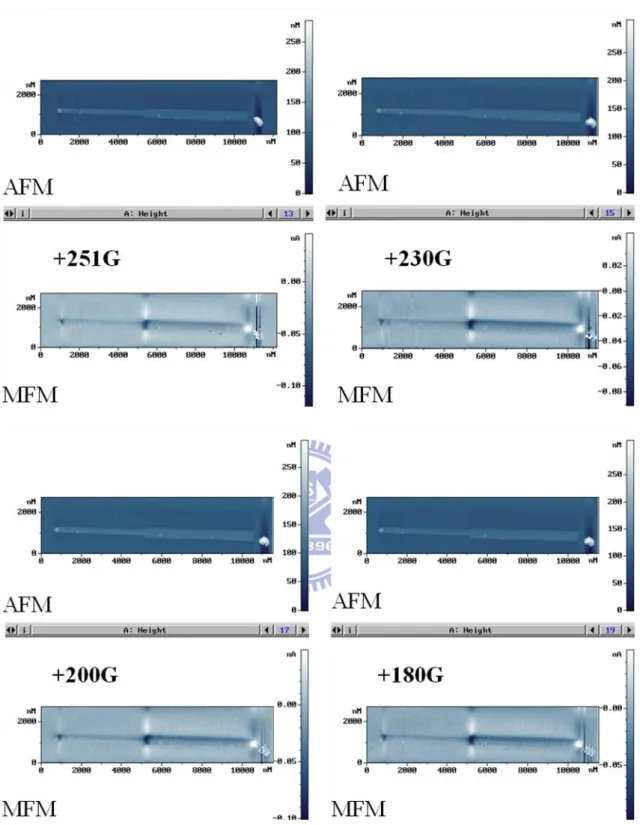
4.1 Quantitative analysis of magnetic reversal in patterned strip wire by magnetic force microscopy 31
4.1 Quantit 4.1.1 Fabrication and measurement of the Permalloy (Py) strip 31
4.1.2 AFM/MFM image at a positive field 32
4.1.3 Observation of the phase magnitude for full loop 34
4.1.4 Evaluation of the individual sections 36
4.1.5 Lists of the phase magnitudes and MFM images 38
4.2.1 Structure of magneto tunnel junction (MTJ) and measurement 45
4.2.2 Temperature-dependent TMR measurement 46
4.2.3 Bias-dependent TMR measurement 51
4.3 Magnetic reversal process and current-induced domain wall motion in ferromagnetic curve- and ring- shape structure 63
4.3.1 AMR behavior and current-induced domain wall motion of single-layered FM ring 63
4.3.2 MR behavior in FM/N/FM tri-layered-ring spin valve 66
4.4 Determining vortex chirality in ferromagnetic ring by lateral spin valve 71
4.4.1 Structure of ring-wire lateral spin valve 71
4.4.2 AMR measurement of the individual ring 73
4.4.3 NLSV measurement and comparison with AMR result 75
4.4.4 Comparison with the wire spin injector 81
4.4.5 Vortex chirality detection by local lateral spin valve 82
4.5 Observation of Hall-like signal in all-metal lateral spin valve 87
4.6 Observation of Anomalous Hall effect in Cu-Py-crossed structure with in-plane magnetization 90
4.6.1 Proposal of Cu-Py-crossed four-terminal Hall device 90
4.6.2 Observation of size-dependent ΔR 92
4.6.3 Proposal of the detailed geometry explaining the origin of ΔR 95
4.6.4 Estimation of AHE in Py 97
4.6.5 Estimation of ordinary Hall effect in Cu 98
4.6.6 Estimation of inverse Spin Hall effect (ISHE) in Cu 99
Chapter 5 Conclusions 101
Reference 103
List of Publication 112
VIII
List of Figures
2.2-1 11 First observation of reproducible, large room temperature MR in a CoFe/Al2O3/Co MTJ. The arrows indicate the relative magnetization orientation in the CoFe and Co layers. After Moodera et al. [109].
2.2-2 14 Spin polarization of the tunneling conductance as a function of the normalized
potential barrier height for various values of k-/k¯. After Slonczewski [19]. 2.2-3 15 Temperature dependence of TMR for a Co/Al2O3/Co MTJ (circles) along with
a fit to the model of Shang et al. [28] (solid line).
2.2-4 16 Original demonstration of the tunneling magnetoresistance effect. The relative conductance change due to an applied magnetic field versus applied bias in a Fe/Ge/Co junction at 4.2 K. After Julliere [17].
2.2-5 18 The bias dependence of (a) the dI/dV in the AP (solid line) and P (dotted line) configurations, and (b) TMR. Arrows mark the local minima in the AP and P configurations. (c) The energy-dependent DOS function [N(Ex)] for P (squares) and AP (circles) configurations. (d) The fitted energy-dependent DOS for FeNi majority (solid squares), FeNi minority (solid circles), Co majority (open squares), and Co minority (open circles). After Xiang et al. [38-39].
2.3-1 20 Illustration of the Hall Effect.
2.3-2 21 Hall effect in ferromagnetic materials. After Volmera et al. [113].
2.4-1 22 Illustration of DOS in a ferromagnet (a) and nonmagnet (b).
2.4-2 23 Illustrations of the spin splitting in the chemical potential induced by spin
injection.
2.4-3 23 (a) SEM image of the mesoscopic spin valve junction. The two wide horizontal strips are the ferromagnetic electrodes Py1 and Py2. The vertical arms of the Cu cross (contacts 3 and 8) lie on top of the Py strips; the horizontal arms of the Cu cross form contacts 5 and 6. Contacts 1, 2, 4, 7 and 9 are attached to Py1 and Py2 to allow four terminal AMR measurements of the Py electrodes. (b)
Schematic representation of the non-local measurement geometry. Current is entering from contact 1 and extracted at contact 5. The voltage is measured between contact 6 and contact 9. (c) The results of nonlocal measurements. Upper curve: An increase in resistance is observed, when the magnetization configuration is changed from parallel to anti-parallel.The solid (dashed) lines correspond to the negative (positive) sweep direction. Middle and bottom curves: The minor loops. After Jedema [45].
2.5-1 25 Reversal process of a ferromagnetic ring. Switching sequence is from left to the right sides. The small circles indicate domain walls. The left ring is the first “onion” state also named “forward onion”. Vortex state (middle) can either be CW or CCW. The right is the reverse onion state.
2.5-2 25 SEM micrographs of rings (a) before and (b) after deposition. After Rothman, et al. [94]. (c) and (d) Typical in-plane MOKE hysteresis loops measured on rings with the same outer and inner diameter of 700 nm and of 300 nm, respectively, but for different thickness of (c) 50 nm and (d) 20 nm. (i) and (ii) represent the forward and vortex state. (e) and (f) Calculated hysteresis loops. After Li, et al. [116].
2.5-3 26 Transverse MR curves of Permalloy ring obtained by (a) theoretical and (b) experimental methods. The spatial relationship between the domains and leads is shown in the inset. The metastable states observed in the sweep-down process are schematically represented in the lower part of each figure. After Lai [101].
3.1-1 28 SEM image of the pad substrate. There are 16 contact pads (labeled by numbers)
on a chip substrate. The four rings at the center are magnetic patterns.
3.2-1 29 Schematic illustration of AFM measurement system.
4.1-1 31 SEM image of the pattern with different widths of strip wire.
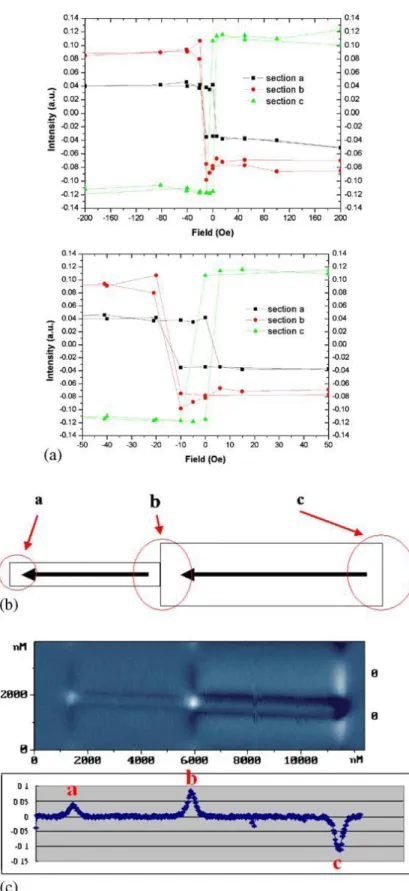
4.1-2 33 AFM/MFM image and MFM magnitude of phase. (a) AFM image (upper), MFM image (middle) and a profile (lower) of line scan in MFM image which was observed at a 140 Oe field which was initially at 250 Oe and varied to –250 Oe. (b) A schematic diagram of the magnetic configuration in accordance with that in (a).
X
4.1-3 35 Phase magnitude for full loop and MFM image at a negative field. (a) Magnetic hysteresis loops (upper) for different local sections presented in values of phase; its zoom in (lower). (b) Schematic diagram of the configuration of the magnetization in the magnetic process of –20 to –200 Oe. (c) MFM image (upper) at –200 Oe and profile (lower) of the line scan in the MFM image. 4.1-4 36 Phase Intensity (absolute value) varying with distance in the pattern near the
magnetic saturation (20 ~ 200 Oe and -20 ~ -200 Oe).
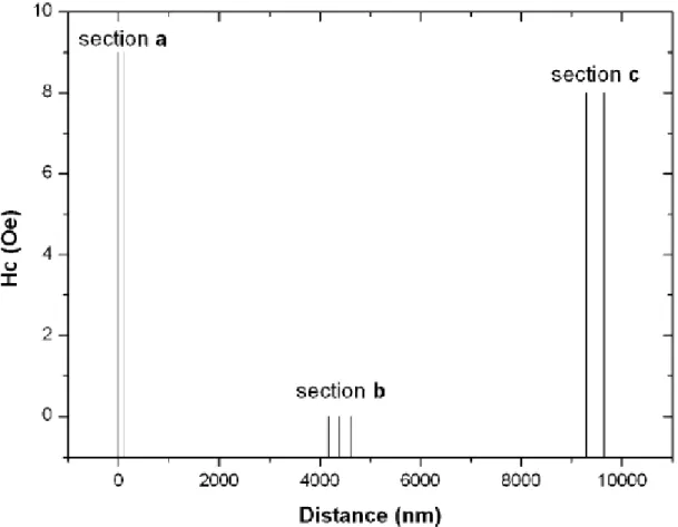
4.1-5 37 The switching field (or coercive force) Hc for each individual local section. 4.1-6 38
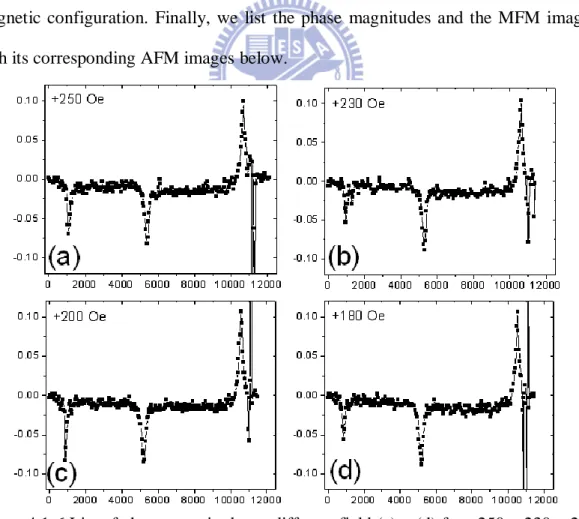
List of phase magnitudes at different field (a) ~ (d) for +250, +230, +200, and +180 Oe. 4.1-6 39
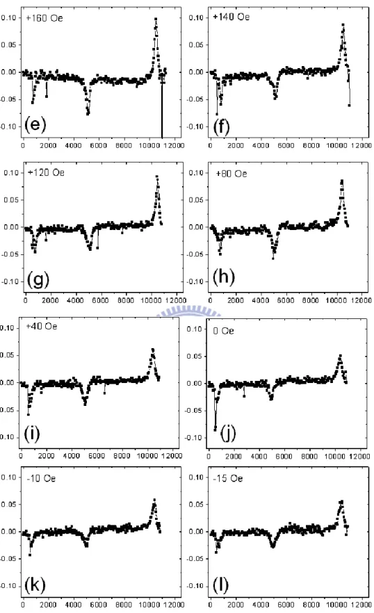
List of phase magnitudes at different field (e) ~ (l) for +160, +140, +120, +80, 40, 0, -10, and -15 Oe.
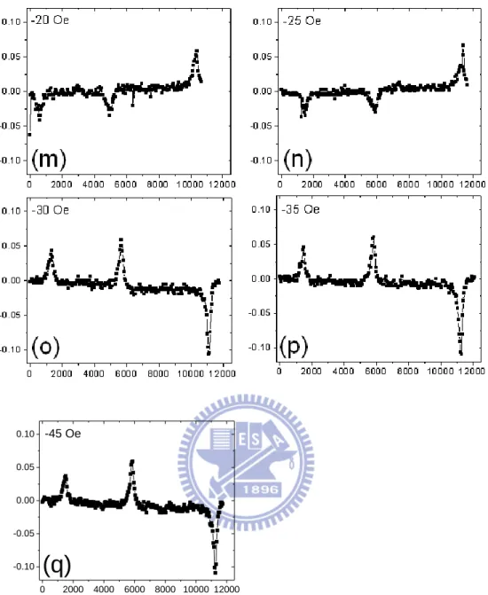
4.1-6 40 List of phase magnitudes at different field (m) ~ (q) for -20, -25, -30, -35, and -45 Oe.
4.1-7 41 List of AFM/MFM images at different field: +250, +230, +200, and +180 Oe. 4.1-7 42 List of AFM/MFM images at different field: +160, +140, +120, and +100Oe. 4.1-7 43 List of AFM/MFM images at different field: +80, 40, 20, 0, -10, and -15 Oe. 4.1-7 44
List of AFM/MFM images at different field: -20, -25, -30, -35, and -45 Oe. 4.2-1 46
Layered structure and lateral size of the MTJ cell.
4.2-2 47 Typical TMR minor loops measured at 50 mV and room temperature.
4.2-3 48 Temperature dependence of TMR loop.
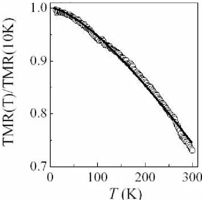
4.2-4 48 Temperature dependence of TMR ratio.
4.2-5 49 Temperature dependence of resistance for P and AP configuration.
4.2-6 49 Comparison of Δ R and MR %.
4.2-7 50 Coercivities variation with temperature. Left: original value. Right: normalized
value.
4.2-8 50 Annealing effect on resistance.
4.2-9 51 Annealing effect on MR ratio.
4.2-10 52 Series of bias-dependent MR loops. (a)~(d) for bias voltage of 5 mV ~ 250 mV. 4.2-10 53 Series of bias-dependent MR loops. (e) ~ (j) for bias voltage of 300 mV ~ 1.2 V. 4.2-10 54 (k) full range.
4.2-11 55
I-V curve for the MTJ device measured at 25℃. 4.2-12 55
Dynamic conductance dI/dV. Derived from Figure 4.2-11 by differentiating I with V.
4.2-13 57 Bias dependence of resistance.
4.2-14 57 Bias dependence of Δ R and MR ratio.
4.2-15 58 I-V curve dependence on temperature. (a) Full range (b) zoom in range from 0.4
V to 0.8 V.
4.2-15 59 (c) zoom in range from -0.4 V to -0.8 V.
4.2-16 59 Temperature dependence of dynamic conductance.
4.2-17 60 Temperature dependence of resistance.
4.2-18 60 Temperature dependence of MR ratio.
4.2-19 61 Comparison between positive and negative voltage polarities of dynamic
XII
4.2-20 62 MR ratio dependence on temperature and bias voltage.
4.3-1 63 AMR measurement of a single-layered Py ring with thickness 40 nm and width 225 nm. The measureing current was 10μA at room temperature. The inset is the SEM image of the sample and the direction of applied field is indicated by the double-head arrow.
4.3-2 64 The AMR minor loop. The arrows indicate the direction of field sweeping. 4.3-3 65 Field-dependent current-induced domain wall motion measurement.
4.3-4 66 Field dependence of critical current density Jc.
4.3-5 67 (a) MR measurement of Py/Cu/Py tri-layered-ring Spin valve. The inset is the full loop. Each circle labeled with number represents a magnetic configuration (or state) which is shown in (b). The single-head arrows indicate the sweep direction. (b) Illustration of each magnetic configuration. The numbers correspond to the labeled circles in (a). The upper ring represents the Py-10nm layer (soft layer), and the bottom one the Py-20nm (hard layer).
4.3-6 69 Minor loop of the measurement of Py/Cu/Py tri-layered-ring spin valve initially saturated in positive field. The arrows indicate the field sweep directions. The circle represents the intermediate state illustrated in the inset. The upper ring represents the Py-10nm layer (soft layer), and the bottom one the Py-20nm (hard layer).
4.4-1 72 SEM image of the lateral spin-valve structure. The premalloy (Py) ring and the Py narrow wire are indicated by the arrows. Cu contacts are labeled as 1 through 8. The double-headed arrow on the left side defines the direction of applied field.
4.4-2 74 (a) The AMR loop of the ring. The arrows indicate the direction of the proceeding process on the loop. The left inset shows the full range of field -1500 ~ +1500 Oe. Vortex directions are schematically indicated in the right inset. Each number with its solid circle is employed to represent each magnetization state and the sequence in process, which is also shown in schematic diagram (b) and (c), in which, the magnetization reversal process is
schematically represented.
4.4-3 76 (a) The full MR loop of the NLSV device (top curve) and the minor loops (middle and bottom curves). The arrows indicate the direction of the proceeding process on the loops. The numbers (correspondent with that in (b) and (c)) represent the sequence in reversal process and the magnetic configurations of the NLSV. (b) Magnetic configurations in the reversal process from positive field to negative. (c) The same as (b) but in reverse sweep.
4.4-4 78 (a) The full MR loop of the NLSV device (top curve) and the minor loops (middle and bottom curves). The arrows indicate the direction of the proceeding process on the loops. The numbers (correspondent with that in (b) and (c)) represent the sequence in reversal process and the magnetic configurations of the NLSV. (b) Magnetic configurations in the reversal process from positive field to negative. (c) The same as (b) but in reverse sweep.
4.4-5 79 The NLSV loops for the probe arrangement in which the current probes were set as 7 and 8. The depictions for the arrows are the same with that in Figure 4.4-3 and Figure 4.4-4. (a) The CCW-CW loop: CCW in sweep from positive to negative field (forward sweep); and CW in the opposite (backward) sweep (b) The CCW-CCW loop: CCW in both forward and backward sweeps.
4.4-6 81 SEM image of a wire-ring lateral spin valve with multi terminals.
4.4-7 82 Results of NLSV measurement for device in Figure 4.4-6.
4.4-8 85 (a) SEM image of wire-ring spin valve. The numbers indicates the four terminals. (b) Schematic illustrations of the two different voltage probe arrangements. Left: alternative geometry, right: the conventional nonlocal geometry as in the previous section.
4.4-9 86 MR measurement of a wire-ring device. The thickness is 22nm for Py, and the width is 120 nm for the wire and 150 nm for the ring with an outside diameter of 1.7um. The wire-ring space is about 40nm, and is bridged by a diffusive channel (Cu) with 170nm in width and 50nm in thickness. (a) Measurement in alternative arrangement with DC current 500 μA. The numbers indicate each magnetic state in accordance with that in (e). The inset illustrates electrodes arrangement and the relative direction of applied field. (b) Measurement of
XIV
conventional AMR for the ring, with DC current 20μA. (c) and (d) Minor loops to approach the switching field from vortex state to reverse onion state. Before switching (c), and after switching (d). (e) schematic illustrations for the reversal process of the device. The numbers are in accordance with that in (a).
4.5-1 89 MR measurement of the same one two-wire device [(a)~(c)] with DC 500 μA. The thickness is 20nm for Py, and the width is 110 nm for the injector and 200 nm for the dtector. The space is about 85nm. The diffusive channel is 210 nm in width and 66nm in thickness. (a) Nonlocal arrangement. (b) Arrangement without voltage probe contact on the detector. (c) Alternative arrangement. (d) MR measurement of single Py wire with AC 150μA. The Py wire is 30 nm in thickness and 220 nm in width. Diffusive channel is 44 nm in thickness and 200 nm in width.
4.6-1 91 (a) 3D geometry of Cu-Py-crossed structure. The direction is denoted by the 3D coordinate. (b) Top view of the device. Upper-left: the original geometry of Jedema’s “contact“ measurement. Upper-right: geometry in the present work. All the directions are relative to the coordinate (bottom-left). Bottom-right: Schematic MR loop. Both geometries exhibit the same configuration of this MR loop. ΔR is defined as the difference in resistance between positive and negative magnetization at 0 Oe.
4.6-2 93 Measured MR loops of device for positive (a) and negative (b) current. The thickness is 65 nm for Cu, and 31 nm for Py. The insets denote the arrangements of current and voltage probes, and direction of applied field. To clearly present the polarity of measured voltage, resistance is calculated by dividing the measured voltage by the absolute value of current, R=V/|I|. (c) Resistance recorded at 0 Oe, with successively alternating magnetization of Py. The odd numbers represent positive magnetization, and the evens represent negative one. (d) Current-dependent ΔR.
4.6-3 94 Cu-width-dependent ΔRs for differently constant widths (a) 200 nm (b) 420 nm and (c) 700 nm of Py wires. (d) Merging all data of (a), (b), and (c). The solid-down triangles represent the estimated values by our roughly simple model. (e) Py-width-dependent ΔRs for differently constant widths (165 nm and 145 nm) of Cu. All the thicknesses are 50 nm for Cu, and 20 nm for Py.
4.6-4 96 Detailed geometry to explain the generated AHE. Left: with electron flow in +Y
and Mx in –X, positive and negative charges are respectively induced on top and bottom surfaces of Py layer. Right: with MX reversed, the polarity of charge accumulation also reverses. The horizontal distance between the two vertical dashed lines denotes the width of Cu.
4.6-5 98 Left: Measurement of Hall effect of Cu. Right: Geometry illustrating the
required effective field for ordinary Hall effect to induce ΔR in Cu.
4.6-6 100 Geometry of ISHE. (a) Top view. (b) View in X-Z plane. (c) View in Y-Z plane. 4.6-7 100 Geometry of ISHE with perpendicular magnetization and spin-current transport in plane. The d in plane denotes the distance for spin to diffuse from ferroganet into diffusive channel (here is Au) and to be sensed by voltage electrodes. After Seki [67].
List of Tables
XVI
List of Symbols
Eex exchange energy Jex exchange integral
Si, Sj, Si, Sj angular momentum vectors of spins
φ the angle between two spins
M , M magnetization d E demagnetizing energy d H demagnetizing field Nd demagnetizing factor
Ek crystalline anisotropic energy
K0, K1, K2 crystalline anisotropic coefficient
α 1,α 2,α 3 cosines of angles between the magnetic moment and crystal axes Ez Zeeman energy
m , m magnetic moment
ex
H external field
GP conductance for parallel alignment
GAP conductance for antiparallel alignment
i
,i “tunneling” density of states of the ferromagnetic electrodes (designated by index i = 1, 2) for the majority- and minority-spin electrons
RP resistance for parallel alignment
RAP resistance for antiparallel alignment
Pi polarization of the ferromagnetic electrodes (designated by index
i = 1, 2)
P effective spin polarization of tunneling electrons decay constant of wave functions into the barrier
me mass of electron Plank constant
EF Fermi energy barrier height T temperature
A parameter of Bloch T3/2 law
v volume
E, Ex energy of electron (in x direction)
V applied bias, voltage
) (
),
(E f E eV
f Fermi distribution function J, j current density
) (Ex
N density of states (DOS) as a function of Ex
, 0, resistivity
I current VHall Hall voltage
RHall Hall resistance
αHall Hall coefficient
αE anomalous Hall coefficient
n ,n concentrations of up- and down-spin electrons in ferromagnets ρH Hall resistivity
t thickness W width αH Hall angle
λ spin diffusion length
1
CHAPTER 1
Introduction
In the past decades, magnetoelectronic device has attracted much attention both in the applications to spin electronics (or spintronics) and in the fundamentals of spin physics. Its versatile applications in information storage, non-volatile memory, and magnetic sensors have been well studied and developed. With the property in which resistance changes from one level to the other one, multilayered spin valves such as giant magnetoresistance (GMR) and magnetic tunnel junction (MTJ) have been successfully implanted as the memory cell [1-2]. In spite of these devices operating based on clear switching of electric resistance and converting to digital signals of “1” or “0”, the physical background of resistance switching actually originates from the magnetization states of the individual magnetic layers in the multilayered devices. Hence, not only the mechanism of spin transport in magnetoelectronic device but also the magnetization reversal process in ferromagnet need to be studied in detail.
Micromagnetics was, therefore, established to investigate the magnetization reversal process, magnetic domain, and domain wall in micro- or nano-scale ferromagnets; and many experimental studies on magnetic thin-film patterns were also reported [2-12]. With the advantages of direct relation to the distribution of magnetization in real space, magnetic force microscopy [13] (MFM) is an effective tool to observe magnetic image of micromagnetic structure in thin-film patterns [4, 9]. In addition, combined with the real-time sweeping magnetic field, the in-situ detection of MFM images can also investigate the process of magnetization reversal [14-16]. Among these studies, quantitative MFM analysis [16] reveals the magnetization reversal process for local parts of a patterned magnetic film by using the statistical calculating of phase shift, and hence promotes MFM usage to relevant
studies.
Unlike the clear understanding on the relations between magnetic images and magnetic structure, the indirect relation between magnetoresistance (MR) signal and magnetic structure, usually cannot be intuitively understood. However, MR measurement provides a more sensitive reflection from the interactions between conducting spin-polarized electrons and local moments in magnetic materials. Besides, in practical applications of magnetoelectro devices, information transport and transmission of actuating energy are mainly based on the electrical operation. Therefore, with both interests in physical origin and feasible applications, a variety of MR phenomena have always been the attractive topics in spintronics.
As the promising applications to spintronics and interests on physics, tunnel magnetoresistance (TMR) phenomena and MTJ devices have caught much attention and many studies have been carried out. Julliere [17] first dedicated to the MTJ experiments and proposed the first theoretic model describing the origin of TMR. According to his assumptions, spin of electrons is conserved during the tunneling process. It infers that up-spin and down-spin electrons tunnel the barrier independently with each other, and hence the conductance occurs in the two independent spin channels. Moreover, the conduction of each spin direction is proportional to the densities of states of that spin in each electrode. This model successfully explained the common TMR phenomenon that the conducting current is larger for parallel alignment of the two ferromagnetic layers than antiparallel one of that, but did not provide the information describing bias voltage and temperature dependence of TMR ratio (%). Julliere’s contribution inspired other researchers to further investigate in this field. Although the results were not reproduced by others and Julliere’s model is not accurate for realistic TMR phenomena, this simple two-current model still provides a substantial understanding on TMR and even used to
3
interpret the similar phenomenon of GMR [18]. Later in 1989, Slonczewski [19] proposed the first accurate theoretical explanation of TMR. By extending the free electron model [20], he proposed that, the polarization of tunneling electrons depends not only on the density of states at that ferromagnet, but also on the height of the tunnel barrier. For these free electron models, however, the lattice structure of ferromagnetic electrodes and the variation of the band structure near the insulating barrier are not considered, hence the predictions for TMR are quantitatively unreliable. The most common property for MTJ is the TMR decreasing with increasing bias voltage and temperature. Zhang et al. [21] proposed that spin excitations localized at the interface between ferronagnet and tunneling barrier cause the decrease of TMR ratio. This model was later used by Han et al. [22] to study the conductance and magnetorsistance as a function of voltage and temperature for Co75F25/Al2O3/Co75Fe25 tunnel junctions. Another mechanism, which could contribute to the voltage dependence of conductance and TMR, is related to the electronic structure of the ferromagnets [23-25]. LeClair et al. [26] proposed a relationship between the magnetotransport properties and the calculated density of states (DOS) for the two different crystallinities of Co. Another crystalline-dependent TMR were also reported [27]. Shang et al. [28] assumed that spin polarization decreases with increasing temperature due to spin-wave excitations, as does the surface magnetization. They then performed the work with fitting to the well known Bloch T3/2 law, and obtained a satisfactory explanation for the temperature dependence of TMR. Other studies on explanation by Bloch T3/2 law were also discussed [29-36]. By modifying Brinkman model [37], Xiang et al. [38-39] calculated the bias dependence of DOS for majority and minority spin bands by fitting to the measured resistance, and named the conductance minima shifts (CMS) which can also be correlated to the voltage dependence of DOS. The similar fitting works were also carried out by other
researchers [31, 40-43]. For MTJ devices during operation, the possibly encountered high temperature could be near 70 ~ 100 ℃. It is our interest to study the temperature dependence of TMR for MTJ devices around this range of temperature to examine the thermal stability of the devices.
In addtion to the spin-dependent tunneling, other phenomena of spin transport such as spin injection and accumulation in normal metal also attract much attention due to the interests in physics and the applications to spintronics. It was Johnson and Silsbee [44] who first demonstrate the spin injection into normal bulk metals. Since then, spin injection into nanometer-sized patterns of a variety of normal metals such as Cu, Al, Au, and Ag [45-60] has been achieved. The description of theoretical model for spin injection dates back to Fert and Campbell [61]. Van Son et al. [62] extended the model to describe transport through ferromagnet-normal matal (F/N) interface. Later, Valet and Fert [63] applied the model based on Boltzamann transport equation to describe the effect of spin accumulation and current-perpendicular-plane GMR.
The significant experiments of another spin transport phenomenon, Spin Hall effect (SHE), has been demonstrated in metallic system [64-67] latter than previously mentioned nonlocal measurement of spin accumulation because the observation of SHE requires advanced experimental technique. However, SHE has been theoretically predicted four decades ago [68]. Later in 1999, Hirsch [69] developed the phenomenological theory with impurity scattering, and then Zhang [70] extended it to the diffusive transport regime. SHE describes a spin current generated in the transverse direction of a charge current and a spin accumulation at lateral boundaries of that conductor. For nonlocal measurements or the crossed geometry, SHE could more or less contribute to the measured signal. Therefore, one might consider and evaluate the magnitude of signal generated by the SHE.
5
domain wall devices are more complicated in reversal process usually associated with single domain wall (bi-domain) or multi domain walls. Hence, the understanding on domain wall motion and the driving source of motion is an important topic for the research and development of domain wall devices. Parkin [71-72] proposed the racetrack memory based on domain wall motion. Moreover, the feasibility to logic gates has also been reported [73-75]. The common feature of these studies is that the ferromagnetic patterns carrying domains and domain walls are narrow wires either in straight- or curved- line shapes. The narrow wire makes domain wall and domain-wall motion clearly defined due to the shape anisotropy along the directions of curve or straight line. In addition, for a curve shape, it is easily for one to manipulate the initial domain wall position by properly choosing the relative direction between the pattern and the applied field. This useful approach has been achieved to study the phenomenon of domain wall motion in narrow wires [76-79]. As the physical interest and the requirement of electric operation for a magnetoelectro device, the phenomenon of current-induced (or current-driven) domain wall motion have also given rise to a great interest to explore for single-layered ferromagnetic narrow wires [80-85]. For these investigations, the approaches to detect domain wall motion are MFM and AMR measurements which may be constrained by the electric operation when used as a device. For tri-layered (ferromagnetic/normal-meteal/ferromagnetic; F/N/F) spin valves [86-90], although the measurement fits to the application of the device, the tri-layered structure makes the behaviors of domain wall motion more complicated since the interaction between the two ferromagnetic (FM) layers affects the domain wall motion which is different from that in single-layered FM.
The vortex state of a ferromagnetic ring features a bi-direction of degeneracy: clockwise (CW) or counter clokwise (CCW). This chirality could serve as a memory bit by considering the direction CW or CCW as “1” or “0” signal. Besides, with its
advantages of the almost zero stray filed out of the ring structure, FM-ring memory cell can be a stable and low noise device. Therefore, FM ring-shaped structure has attracted much attention and many studies on basic behaviors of reversal process of FM rings have been carried out [91-95]. Since the transition of onion-to-vortex in ring structure is completed by domain wall propagation, the behavior the domain wall motion plays an important role in FM-ring device when observing the reversal process in tri-layered [96-100] or single-layered [101-102] rings by MR measurement. The current-induced domain wall motion in FM ring was also performed for single-layered [102] and tri-layered [103] structures. The detection of vortex chirality of FM rings can be performed by tri-layered structure [98-100, 103]. For the single-layered, however, the measurement with only AMR provides no crucial information for determining the chiralities. It was Kimura [6, 104] first carried out the detection of vortex chirality of a single-layered structure by using nonlocal spin valve (NLSV) measurement to sense spin accumulation in the normal-metal diffusive channel and determine the spin orientation of the spin injector adjacent to the spin diffusive channel.
In this dissertation, we review the researches related to the voltage and temperature dependent TMR of MTJ devices, reversal process of magnetic patterns, and spin dependent transport such as spin injection, spin accumulation and AMR behaviors in Chapter 1. The basic theory and some phenomena that relate to the investigations in this dissertation are described in Chapter 2. Chapter 3 presents the principle and methodology of the experiments. In Chapter 4 we discuss the experimental results and compare with the results repeated by other researchers for satisfied explanations. Section 4.1 presents the results of the quantitative MFM analysis. We investigated a magnetic patterned strip with two-different-width parts by analyzing its MFM phase changes, and focused on the two ends of the strip and the region in which the wider
7
part changes to the narrower one. Section 4.2 presents the temperature and voltage dependent TMR measurements of MTJs. The possible physical origins of both dependences were discussed. In Section 4.3, we describe the magnetization states and reversal behaviors of the single-layered Py ring and the tri-layered spin valve Py ring. Inspired by the drawback of the incapability of detecting the chirality of the ferromagnetic rings (mentioned in Sec. 4.3), we further fabricated and measured the nonlocal lateral spin valve (NLSV) including a Py wire and ring to sense the spin accumulation signals and determine the direction of circulating vortex in the ring. The results are shown in Section 4.4. Besides, to obtain the larger spin signals in the lateral spin valve (LSV), we shortened the distance of spin diffusive channel by removing the Cu cross inserted in between the Py ring and the wire. The structure is no longer a nonlocal geometry. However, the spin accumulation can still be detected and enhanced but with an extra signal that exhibits asymmetric MR behavior. In Section 4.5, we tried extracting the spin accumulation signals by replacing the ring with a second wire but in different width with the first one. We then measured the three different geometries in this two-wired LSV. In Section 4.6, we systematically studied the physical origin of the asymmetric signals found in section 4.4 and 4.5. The results of the size dependent measurement suggests the physical origin is most possibly from the anomalous Hall effect of the in-plane magnetization Py wire (the spin injector).
CHAPTER 2
Introduction to Basic Theory and Phenomena
2.1 Magnetic domain and domain wall
A stable magnetic state consists of domains and domain walls existing within a ferromagnetic material (bulk, film, or patterned film) and reaching an equilibrium state without varying with time in macroscopic scale. The stable state is a result of competition among exchange energy, demagnetizing energy, anisotropic energy (usually the crystalline anisotropy), and Zeeman energy in that material in which the total energy stays at the minimum under the stably applied magnetic field.
Exchange interaction and energy The exchange interaction comes from a consequence of a quantum effect that the atomic magnetic moments tend to align to the same direction with each other in ferromagnetic. This interaction affects the alignment between two adjacent spin elements in a short range of few atoms. Hence, the exchange energy of the alignment between two spin elements (usually the atomic magnetic moments) is given by [108]
Eex = -2 Jex Si․Sj = -2 Jex Si Sj cosφ, (2-1)
where Si and Sj represent the angular momentum vectors of two adjacent spins, Jex is called the exchange integral, which occurs in the calculation of exchange effect, and φ is the angle between the two spins.
Demagnetizing energy The demagnetizing energy is caused by demagnetizing field which is induced by the magnetization of a ferromagnet. The direction of the demagnetizing field is usually opposite to the magnetization in the ferromagnet, and
9
hence the field tends towards reducing the total magnetization, i.e., “demagnetizing” the ferromagnet itself. It also gives rise to the shape anisotropy. The energy of the demagnetizing field is completely determined by an integral over the volume of the magnet and can be express as
dv H M Ed
magnet d 2 1 , (2-2) where Hd is demagnetized field and is given by Hd NdM . Nd is thedemagnetizing factor [108] which depends on the geometric shape of the ferromagnet. For a ferromagnetic strip or narrow wire, Nd is very small (Nd << 1) along the direction of wire axis. It results in that the magnetization along the wire direction maintains little demagnetized at the remanence, i.e., most of the moments is aligned to the wire direction in the absence of applied field. With this shape anisotropy, magnetic wires are usually used to study domain wall motion.
Crystalline anisotropy When an applied field turns the magnetization vector of a crystal away from the easy direction in that crystal, the field must do work against the anisotropic force. Hence, there must be crystal anisotropy energy (Ek) stored in the crystal in which the saturated magnetization (Ms) points in a noneasy direction. Ek can be expressed as [108]
Ek K0 K1(1222 2232 3212)K2(122232)..., (2-3) where K0, K1, K2… are constants for a particular material. Higher powers are generally neglected. K0 is independent of angle and is usually ignored. α 1, α 2, and α 3 are the cosines of angles between the magnetic moment and crystal axes.
Zeeman energy The Zeeman energy (Ez) is resulted from the interactions between magnetic moments and an applied field. For a single moment, the energy is
expressed as cos ex ex z m H mH E , (2-4) where Hex is the externally applied field, and θ is the angle between the moment and the applied field. For the whole volume of a ferromagnet, the Zeeman energy per unit volume is then calculated by integrating each local magnetization over the whole volume and is given by
dv H v M
11
2.2 Magnetic tunnel junction (MTJ) and Tunnel Magnetoresistance (TMR)
The phenomenon of TMR is from the measurement for an MTJ, which consists of two ferromagnetic layers separated by an insulating tunnel barrier. The insulating layer is thin enough (usually few Å ~ 15 Å) for conducting electrons to quantum mechanically tunnel through the barrier. When a bias voltage applied across the MTJ, a net tunneling current is flowing through the junction. The measured MTJ resistance is usually higher when the two ferromagnetic layers are in anti-parallel alignment than that when they are in parallel alignment. This is the general TMR phenomenon observed. Figure 2.2-1 shows a TMR loop of a psuedo-spin-valve MTJ.
Figure 2.2-1 First observation of reproducible, large room temperature MR in a CoFe/Al2O3/Co MTJ. The arrows indicate the relative magnetization orientation in the CoFe and Co layers. After Moodera et al. [109].
2.2.1 Julliere’s Model
Julliere [17] assumed that tunneling of up-spin and down-spin electrons are two independent processes, so that the conductance occurs in the two independent spin channels. The assumption also mentioned that conductance for a particular spin orientation is proportional to the product of the effective (tunneling) density of states of the two ferromagnetic electrodes. According to these assumptions, the conductance for the parallel and antiparallel alignment, GP and GAP, can be written as follows:
1 2 1 2 P G , (2-6a) 12 12 AP G , (2-6b) where iand iare the tunneling density of states (DOS) of the ferromagnetic electrodes (designated by index i = 1, 2) for the majority- and minority-spin electrons. According to the majority of researchers, the TMR can be defined as the conductance difference between parallel and anti-parallel magnetizations, normalized by the anti-parallel conductance, i.e.
P P AP AP AP P R R R G G G TMR . (2-7) With Eqs. (2-6) and (2-7), Julliere’s formula can be expressed as
2 1 2 1 1 2 P P P P T M R , (2-8)
which expresses the TMR in terms of the effective spin polarizations (SPs) of the two ferromagnetic electrodes i i i i i P , (2-9) where i = 1, 2.
13 2.2.2 Slonczewski’s model
Slonczewski [19] considered the tunneling between two identical ferromagnetic electrodes separated by a rectangular potential barrier assuming that the ferromagnets can be described by two parabolic bands shifted rigidly with respect to one another to model the exchange splitting of the spin bands. In the limit of thick barrier, he found that the conductance is a linear function of the cosine of angle θ between the magnetic moments of the films,
G()G0(1P2c o s). (2-10)
Here P is the effective spin polarization of tunneling electrons given by
k k k k k k k k k k P 2 2 , (2-11) where is the decay constant of the wave function into the barrier which is determined by the potential barrier height , k (2me/2)(EF). In the limit of a high barrier it tends to unity reducing Slonczewski’s result for TMR to Julliere’s formula. However, if the barrier is not very high and the decay constant is comparable to or less than the wave vectors of electrons in the ferromagnetic metals, the magnitude of TMR decreases with decreasing and even changes sign for
Figure 2.2-2 Spin polarization of the tunneling conductance as a function of the normalized potential barrier height for various values of k-/k¯. After Slonczewski [19].
2.2.3 Temperature dependence of TMR
In all tunnel junctions the TMR decreases with increasing temperature. Shang [28] et al. assumed that the tunneling spin polarization P decreases with increasing temperature due to spin-wave excitations, as does the surface magnetization. They thus assumed that both the tunneling spin polarization and the interface magnetization followed the same temperature dependence, the well-known Bloch T3/2 law, M(T) = M(0)(1-AT3/2). By fitting parameter A, Shang et al. obtained a satisfactory explanation for the temperature dependence of TMR, as demonstrated by the fitting in Figure 2.2-3.
15
Figure 2.2-3 Temperature dependence of TMR for a Co/Al2O3/Co MTJ (circles) along with a fit to the model of Shang et al. [28] (solid line).
2.2.4 Voltage dependence of TMR
In most MTJ’s the magnitude of TMR decreases strongly with increasing bias voltage, similar to that observed originally by Julliere (Figure 2.2-4). Zhang et al. [21] proposed that spin excitations localized at the interface between ferronagnet and tunneling barrier cause the decrease of TMR ratio. However, experiments by Wulfhekel et al. [110] seem to be inconsistent with this plausible explanation. Here we introduce another explanation by Xiang et al. [38-39]. By modifying the Brinkman model [37], they calculated the bias dependence of DOS for majority and minority spin bands by fitting to the measured resistance, and named the conductance minima shifts (CMS) which can also be correlated to the voltage dependence of DOS.
Figure 2.2-4 Original demonstration of the tunneling magnetoresistance effect. The relative conductance change due to an applied magnetic field versus applied bias in a Fe/Ge/Co junction at 4.2 K. After Julliere [17].
Brinkman model and its modification Brinkman’s model [37] calculates the tunnel barrier conductance of a metal-insulator-metal structure. Consider two metals a and b separated by an arbitrary potential barrier (x) . Assuming the WKB approximation inside the barrier the tunneling current density is given by [111]
i k x b a xN E N E eV E f E f E eV dE e j 4 ( ) ( )( ) [ ( ) ( )] , (2-11)where Na(E) and Nb(E) are the density of states for a given transverse
momentum ki and total energy E for systems a and b, respectively. f(E) is the usual Fermi distribution function. Ex is the total energy in the direction perpendicular to the
barrier, (Ex) is the tunneling probability which has the form
d x e x m x V E dx h C E 0 2 / 1 ) ]} ) , ( [ 2 { 2 exp( ) ( , (2-12)17
where d is the barrier thickness and (x,V) is the barrier height at the voltage V and
the position x in the barrier. The preexponential factor C may depend on Ex.
Xiang et al. [38-39] late introduced the spin- and energy-dependent DOS into Brinkman’s model. The current density is then expressed as
x x d x e xV E dx N E f E f E eV dE m J exp 2 {2 [ ( , ) ]} ( )[ ( ) ( )] 0 2 / 1
,(2-13) where (x,V)1 (x/d)(2 eV 1), 1 and 2 are the barrier height at each interface, d is the barrier width, V is the applied bias, and x is the distance from the interface with barrier height 1. N(Ex) is the DOS function and can be expressed as ) ( ) ( ) ( ) ( ) (E N1 E N2 E eV N1 E N2 E eV N x x x , (2-14a) ) ( ) ( ) ( ) ( ) (E N1 E N2 E eV N1 E N2 E eV N x x x . (2-14b) (2-14a) is for parallel configuration, and (2-14b) for anti-parallel configuration. Here, 1 and 2 represent the two FM electrodes.
With the extended Brinkman model, the DOS of Co and FeNi electrodes was derived (cases of Co(3.6nm)/AlOx/Co(3.6nm) and FeNi(8nm)/AlOx/FeNi(16nm) in [39]), and are shown in Figures 2.2-5 (c) and (d). It is clear that the DOS functions in both configurations are bias dependent. In the negative bias region of the parallel (P) configuration, the DOS function decreases with increasing bias. This results in a CMS to the left. Compared to P configuration, the DOS function in anti-parellel (AP) configuration has a weaker dependence on bias. Thus, not only does the barrier height contribute to the CMS, but the bias dependence of the DOS function also affects the shift. We can see from the experimental results that this contribution is quite significant. Since the bias dependence of the DOS function is different between the P and AP configurations, the shifts in the conductance minima are different. In a symmetrical junction, the DOS function is always symmetric about zero bias.
Consequently there is no CMS.
Figure 2.2-5 The bias dependence of (a) the dI/dV in the AP (solid line) and P (dotted line) configurations, and (b) TMR. Arrows mark the local minima in the AP and P configurations. (c) The energy-dependent DOS function [N(Ex)] for P (squares) and AP (circles) configurations. (d) The fitted energy-dependent DOS for FeNi majority (solid squares), FeNi minority (solid circles), Co majority (open squares), and Co minority (open circles). After Xiang et al. [38-39].
19 2.3 AMR and Hall Effect
In this section, we consider other effects of an applied magnetic field.
Anisotropic magnetoresistance (AMR) AMR describes the effect in which the electric resistance depends on the relative orientation, θ, between the local moment and the direction of charge current in a ferromagnetic material. The phenomenological dependence of the resistance on θ is given by
0 cos2() , (2-15) where 0 is the zero-field resistivity and in which parallel and perpendicular refer to the orientation of the in-plane magnetization and current in the material.
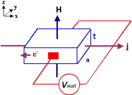
Ordinary and Anomalous Hall effect In 1879, E. Hall [112] discovered that a voltage difference is produced across an electric conductor, transverse to an electric current in that conductor with a magnetic field perpendicular to the current (Figure 2.3-1). The voltage difference or, the Hall voltage (VHall) can be expressed in a phenomenological form, t I H a E VH a l l H a l lH a l l , (2-16) where EHall is the electric field generated in the direction transverse to the current, a is the transverse distance of the conductor, t is the conductor thickness perpendicular to a, I is the electric current, H is the applied magnetic field perpendicular to the current, and α Hall is the Hall coefficient which is usually a constant depending on materials. Since Equation (2-16) describes a linear relationship between VHall and I. We then further derive the Hall resistance, RHall, as
t H I V R H a l l H a l l H a l l 1 . (2-17) This relation indictes that RHall is proportional to the applied field and reciprocal to the
size parameter t in the direction of the field, and is useful for experimental measurement to determine the α Hall of a material. Hence, the Hall resistivity, ρ Hall, can be expressed as
H a l l RH a l lt H a l lH. (2-18) Equation (2-18) describes the linear relation between the Hall resistivity and the applied field. The Hall coefficient α Hall can be either positive or negative, depending on the material type.
Figure 2.3-1 Illustration of the Hall Effect.
We then discuss the Hall Effect in ferromagnetic materials. The Hall voltage consists of a sum of two terms. The first term is proportional to the magnetic field, as we mentioned above, and has been called the ordinary Hall Effect. Its order of magnitude and sensitivity to variations in temperature and in composition are comparable with Hall Effect in non-ferromagnetic materials. The second term is proportional to the magnetization and has been called the anomalous or extraordinary Hall effect. Equation (2-17) can then be extended to a ferromagnetic case [113-115]
( )
1 H M H t I V R Hall Hall E Hall , (2-19)21
where α E is anomalous Hall coefficient, and M(B) is the magnetization which is the function of field. By neglecting the ordinary term, the RHall-B curve exhibits almost a magnetization process like M-B curve since M(B) is directly proportional to the RHall. A measurement of Hall effect in ferromagnets is shown in Figure 2.3-2.
2.4 Spin injection and accumulation in lateral spin valve
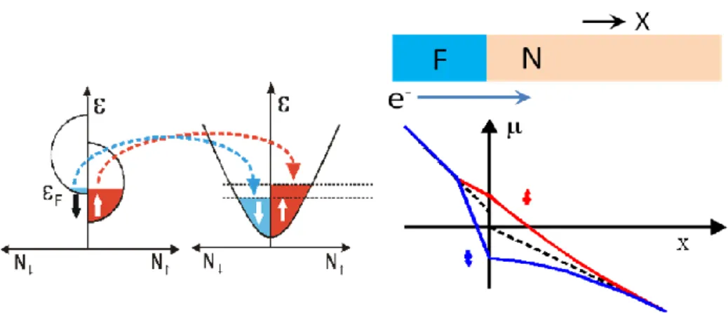
Spin current [56] is generated in a ferromagnet with unequal popularities of conducting up- and down-spin electrons. This inequality is mainly due to the unequal DOS of up- and down-spin bands near the Fermi level (Figure 2.4-1(a)). The spin
current Is can be expressed as S IC PFIC n n n n I , (2-20)
where PF (n n)/(n n) is spin polarization (SP) which is defined by Equation (2-9), n and n are the concentrations of up- and down-spin electrons in the ferromagnet, and IC is the total charge current. Whereas, in nonmagnet (Figure 2.4-1(b)), the DOS is equal for up- and down-spin bands, and the current is un-polarized.
Figure 2.4-1 Illustration of DOS in a ferromagnet (a) and nonmagnet (b).
When the spin current flows across the F/N junction (Figure 2.4-2), however, the spin splitting in the chemical potential is induced in both F and N subsection, and hence the non-equilibrium spin accumulation is induced in nonmagnet. The spin dependent chemical potential without voltage drop due to charge current can be measured by nonlocal spin valve [45].
23
Figure 2.4-2 Illustrations of the spin splitting in the chemical potential induced by spin injection.
Figure 2.4-3 (a) SEM image of the mesoscopic spin valve junction. The two wide horizontal strips are the ferromagnetic electrodes Py1 and Py2. The vertical arms of the Cu cross (contacts 3 and 8) lie on top of the Py strips; the horizontal arms of the Cu cross form contacts 5 and 6. Contacts 1, 2, 4, 7 and 9 are attached to Py1 and Py2 to allow four terminal AMR measurements of the Py electrodes. (b) Schematic representation of the non-local measurement geometry. Current is entering from contact 1 and extracted at contact 5. The voltage is measured between contact 6 and contact 9. (c) The results of nonlocal measurements. Upper curve: An increase in resistance is observed, when the magnetization configuration is changed from parallel to anti-parallel.The solid (dashed) lines correspond to the negative (positive) sweep direction. Middle and bottom curves: The minor loops. After Jedema [45].
2.5 Magnetic reversal process of ferromagnetic ring
During released from saturation to low field, the magnetization of a ferromagnetic ring gradually forms a bi-domain state in which a pair of head-to-head and tail-to-tail domain walls positioned at both sides aligned to the initial saturated direction (Figure 2.5-1). This bi-domain is called “onion” state. It is a consequent result of the shape anisotropy, since most of the local moments are aligned to the perimeter direction of the ring. With the applied field continuing swept to the opposite direction, the two domain walls start moving towards each other, resulting in the annihilation of the domain walls. In this state, all the local moments are still aligned to the perimeter and in the same circulation without domain walls. The whole magnetization is thus in a vortex formation. This state is named “vortex” state. It is reasonably to understand that the chirality of the vortex can either be clockwise (CW) or counterclockwise (CCW), since there is no preference chirality for a symmetric ring. When increasing stronger field magnitude in opposite direction, the vortex state is destroyed and two domain walls nucleate at both sides of the ring aligned to the field direction. Hence, the bi-domain forms again but its magnetization is opposite to that of the first onion state mentioned previously. This state is called “reverse onion” state, whose direction is opposite to the initial saturated field. For clear identification, one can also names the first onion state as “forward onion” state when describing the magnetic switching of a ferromagnetic ring.
However, the size dependence strongly affects the reversal process. With a larger aspect ratio of diameter (or radius) to width of the ring, the vortex state tends to no existence during a regular reversal sequence. Besides, the thinner film of ferromagnetic ring also prefers no existence of the vortex. The switching phase diagrams of the magnetic rings have been reported [91, 93] with varying sizes.
25
Figure 2.5-1 Reversal process of a ferromagnetic ring. Switching sequence is from left to the right sides. The small circles indicate domain walls. The left ring is the first “onion” state also named “forward onion”. Vortex state (middle) can either be CW or CCW. The right is the reverse onion state.
The SEM images and typical magnetic hysteretic loops of ferromagnetic rings are shown in Figure 2.5-2.
Figure 2.5-2 SEM micrographs of rings (a) before and (b) after deposition. After Rothman, et al. [94]. (c) and (d) Typical in-plane MOKE hysteresis loops measured on rings with the same outer and inner diameter of 700 nm and of 300 nm, respectively, but for different thickness of (c) 50 nm and (d) 20 nm. (i) and (ii) represent the forward and vortex state. (e) and (f) Calculated hysteresis loops. After Li, et al. [116].
AMR measurement of ferromagnetic rings has been systematically studied by Lai, et al. [101]. In their studies, the vortex states can be characterized by in AMR loop of a ferromagnetic ring as shown in Figure 2.5-3.
Figure 5.2-3 Transverse MR curves of Permalloy ring obtained by (a) theoretical and (b) experimental methods. The spatial relationship between the domains and leads is shown in the inset. The metastable states observed in the sweep-down process are schematically represented in the lower part of each figure. After Lai [101].
27
CHAPTER 3
Experiments
3.1 Sample preparation
Patterned magnetic thin films in submicron and nano sizes were fabricated mainly by electron beam (E-beam) lithography. These patterned magnetic devices were constructed on SiO2(50 nm)/Si substrates on which electrical contact pads were formed by photolithography. Both E-beam lithography and photolithography were followed by series processes of deposition and lift-off techniques.
Photolithography to fabricate contact pads The SiO2/Si substrates were first coated with positive photoresist (LOR 10B), spined at speed of 4000 rpm for 25 sec, and baked at temperature of 190℃ for 5 min. Then, the substrates was coated S1813 photoresist at the same spin conditions as LOR 10B and baked at temperature of 120 ℃ for 3 min. After exposing and developing, the Au(40nm)/Ti(10nm) films were deposited on the substrates. The lift-off technique was performed to complete the pad patterns as shown in figure. 3.1-1. The EVG620 mask aligner was used as photoresist exposure with intensity = 15 mw/cm2 for 5.7 sec.
E-beam lithography to fabricate magnetic devices The PMMA electron resist were first coated on the pre-deposited pad substrates at the conditions of spin speed = 4000 rpm for 25 sec and baked at temperature of 135℃ for 1hr. The following processes were the same as the photolithography process. E-beam source was provided by an FEI model XL30 SFEG SEM. The exposure dose was 0.3 ~ 0.6 nC/cm depending on the desired widths. Both center-to-center distance and line spacing were 10 nm.
Deposition of thin films DC magnetron sputtering was used to deposit the Cu, and Permalloy (Py: Ni80Fe20), Au, and Ti thin films. The base pressure of the vacuum system was about 5.0 ~ 7.0 × 10⁻⁷ torr, and the working pressure 1.0 ~ 1.2 × 10⁻³ torr with introducing Ar gas into the vacuum chamber.
Ar-ion milling Before depositing Cu leads on magnetic patterns, the Ar-ion beam was used to pre-clean the surface of magnetic thin films at the working pressure of 1.0 × 10⁻⁵
torr.
Fabrication of MTJ The MTJ samples were provided by ERSO, ITRI (Electronics Research & Service Organization, Industrial Technology Research Institude, Hsinchu, Taiwan), and hence detailed manufacturing process of the MTJs we measured is not discussed in this disertation. Instead, the brief processes will be presented in section 4.2.1.
Figure 3.1-1 SEM image of the pad substrate. There are 16 contact pads (labeled by numbers) on a chip substrate. The four rings at the center are magnetic patterns.