342 IEEE ELECTRON DEVICE LETTERS, VOL. 33, NO. 3, MARCH 2012
Asymmetric Carrier Conduction Mechanism by
Tip Electric Field in WSiO
X
Resistance
Switching Device
Yong-En Syu, Ting-Chang Chang, Tsung-Ming Tsai, Geng-Wei Chang, Kuan-Chang Chang,
Jyun-Hao Lou, Ya-Hsiang Tai, Ming-Jinn Tsai, Ying-Lang Wang, and Simon M. Sze
Abstract—Resistance random access memory (RRAM) is a
great potential candidate for next-generation nonvolatile memory due to the outstanding memory characteristic. However, the resis-tance switching mechanism is still a riddle nowadays. In this letter, the switching mechanism is investigated by current–voltage (I–V ) curve fitting in the TiN/WSiOX/Pt RRAM device. The asymmetric phenomenon of the carrier conduction behavior is explained at the high-resistance state in high electric field. The switching behavior is regarded to tip electric field by localizing the filament between the interface of top electrode and insulator.
Index Terms—Nonvolatile memory, resistance switching, tip
electric field, tungsten silicide (WSi).
I. INTRODUCTION
M
ODERN semiconductor nonvolatile memories are scaled constantly to achieve large capacity while device features are approaching the sub-100-nm regime. Nevertheless, for conventional charge-storage-based memories, such as Flash memory, the increasing demands for device densities by scalingManuscript received October 31, 2011; revised December 11, 2011; accepted December 17, 2011. Date of publication February 10, 2012; date of current version February 23, 2012. This work was supported by the National Science Council of the Republic of China under Contract NSC 100-2120-M-110-003. The review of this letter was arranged by Editor C. P. Yue.
Y.-E. Syu and J.-H. Lou are with the Department of Physics, National Sun Yat-Sen University, Kaohsiung 804, Taiwan (e-mail: [email protected]; [email protected]).
T.-C. Chang is with the Department of Physics, National Sun Yat-Sen University, Kaohsiung 804, Taiwan, and also with the Advanced Optoelectronic Technology Center, National Cheng Kung University, Tainan 701, Taiwan (e-mail: [email protected]).
T.-M. Tsai and K.-C. Chang are with the Institute of Materials Science and Engineering, National Sun Yat-Sen University, Kaohsiung 804, Taiwan (e-mail: [email protected]; [email protected]).
G.-W. Chang and Y.-H. Tai are with the Department of Photonics and the Institute of Electro-Optical Engineering, National Chiao Tung Univer-sity, Hsinchu 300, Taiwan (e-mail: [email protected]; [email protected]. edu.tw).
M.-J. Tsai is with the Nanoelectronic Technology Division, Electronics and Optoelectronics Research Laboratories, ITRI, Hsinchu 31040, Taiwan (e-mail: [email protected]).
Y.-L. Wang is with the Taiwan Semiconductor Manufacturing Company, Hsinchu 300, Taiwan (e-mail: [email protected]).
S. M. Sze is with the Department of Physics, National Sun Yat-Sen Univer-sity, Kaohsiung 804, Taiwan. He is also with the Department of Electronics Engineering, National Chiao Tung University, Hsinchu 300, Taiwan, and also with the Department of Electrical Engineering, Stanford University, Stanford, CA 94305-4085 USA (e-mail: [email protected]).
Color versions of one or more of the figures in this letter are available online at http://ieeexplore.ieee.org.
Digital Object Identifier 10.1109/LED.2011.2182600
the dimension are expected to be a major challenge due to the technical and physical limitations. In order to overcome the issue, alternative memory technologies have been widely in-vestigated [1]–[3]. Resistance random access memory (RRAM) is a great potential candidate for next-generation nonvolatile memory due to its superior properties such as simple structure, fast operation speed, low cost, and nondestructive readout [4]–[11]. The WSiOX is chosen for the RRAM switching
layer because tungsten and silicon are compatible with the current complementary metal–oxide–semiconductor process. Heretofore, the resistance switching mechanism is unclear and difficult to confirm. In general, the resistance switching be-havior is considered as a result of the formation and rupture of localized conduction filaments in oxide materials [10]. In this letter, the carrier transport behavior is analyzed by fitting the current–voltage (I–V ) curves to identify the switching mechanism. The asymmetric carrier conduction behavior is observed at the high-resistance state (HRS) in high electric field and explained by the schematic energy band diagram. By the analysis results, the conduction filament theory can be verified.
II. EXPERIMENT
The 30-nm WSiOX film was deposited on a TiN/SiO2/Si
substrate as the resistance switching layer by RF magnetron sputtering using the WSi (W : Si = 1 : 1) target, in Ar/O2=
30 sccm/10 sccm mixed gas ambient with a working pressure of 6 mtorr. The Pt top electrode was deposited on an insulator WSiOX thin film by dc magnetron sputter. Finally, the
pho-tolithography and lift-off technique were employed to shape and complete the Pt/WSiOX/TiN memory cells. The electrical
characteristics were measured for the memory devices with 1-μm2 square cell area by an Agilent B1500 semiconductor
parameter analyzer. During the electrical measurements, dc sweeping and pulse bias were applied to the bottom electrode (TiN) while the top electrode (Pt) was grounded.
III. RESULTS ANDDISCUSSION
The irreversible forming process that formed the conduction path is required to make the as-fabricated memory cells active, operating in dc voltage sweep mode with a compliance cur-rent of 100 μA to prevent the device hard breakdown, shown in the inset of Fig. 1. The repeatable resistance switching
SYU et al.: ASYMMETRIC CARRIER CONDUCTION MECHANISM BY TIP ELECTRIC FIELD 343
Fig. 1. Typical 100-cycle resistive switching I–V curves of Pt/WSiOX/TiN
device. Inset shows the forming voltage of the device.
Fig. 2. Distributions of (a) the resistance states of HRS and LRS and (b) the switch voltage during 100 resistance switching cycles. The reliability of the device: (c) Resistance measurements after voltage pulse cycling and (d) retention behaviors of the HRS and LRS at 125◦C.
between HRS and low-resistance state (LRS) is obtained after the forming process. By sweeping the bias to negative over reset voltage (Vreset), a gradual current decrease is presented
because the conduction filaments are ruptured. The resistance state of the device transforms from LRS to HRS, called “reset process.” Conversely, the conduction filaments are formed, and the cell turns back to LRS while applying a larger positive bias than set voltage (Vset), i.e., “set process.” A compliance
current of 10 mA is assigned to prevent permanent breakdown. Fig. 1 shows the typical 100-cycle I–V characteristic of the Pt/WSiOX/TiN device by dc sweep voltage measurements, and
the device exhibits the bipolar behavior by applying the bias on the TiN electrode.
The distributions of the resistance states and switch volt-age are counted with continuous I–V sweep measurement of 100 cycles, as shown in Fig. 2(a) and (b). Resistance state distribution shows the stable resistance switching behaviors
Fig. 3. Curve fitting of carrier transport analysis in different bias regions and resistance states of WSiOXswitching layer.
and displays the large enough RHRS/RLRS ratio over two
orders apart for the periphery circuits to probe the different resistance states. In addition, the switch voltage distribution shows the over 70% set voltage concentration from 1 to 1.2 V and 79% reset voltage concentration from−0.7 to −0.8 V. Furthermore, the endurance and retention of the Pt/WSiOX/TiN
device are necessary to investigate for nonvolatile memory application. Fig. 2(c) shows the resistance of the HRS and LRS versus the number of pulses. The HRS was set to the LRS by applying a setting voltage of 2 V for 550 ns, while the LRS was reset to HRS by applying −2 V for 2 μs. Both HRS and LRS resistance values were extracted at 0.1 V. The RRAM device can be repeatedly operated over 105cycles, and the RHRSand RLRSremain two orders apart. Fig. 2(d) shows
the variation of the resistance with time at both the HRS and LRS for the Pt/WSiOX/TiN device at 125◦C. After 10 000 s,
the variation of HRS and LRS is very slight. It indicates that the Pt/WSiOX/TiN device has both excellent reliability and
durability.
In order to ascertain the switching mechanism, the I–V curves are fitted to analyze carrier transport of the switching layer, as shown in Fig. 3. Moreover, we explained the mecha-nism by energy band diagram, as shown in Fig. 4. The carrier transport mechanism in LRS is considered as ohmic conduction because the carriers are transported through the continuous filament. The carrier transport mechanism in HRS with lower electric field is dominated by ohmic conduction because the current originates from the internal carrier in the WSiOX, as
shown in Fig. 4. The bias rises continuously, and the relation between ln(I/T2) and the square root of the applied voltage
(V1/2) is linear. Schottky emission is considered as the main
transport mechanism [12]. The major leakage current results from the electron leap across the potential energy barrier by the thermionic effect [as shown in Fig. 4(b) and (e)], while the energy band bending is insignificant. Therefore, the carrier transport mechanism at this bias region complied with the Schottky emission mechanism.
The asymmetric phenomenon of the carrier conduction be-havior is found at HRS in high electric field. At the positive-bias
344 IEEE ELECTRON DEVICE LETTERS, VOL. 33, NO. 3, MARCH 2012
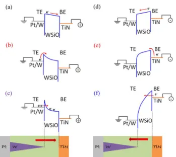
Fig. 4. Corresponding schematic energy band diagram in different bias re-gions and resistance states.
region, the current transportation mechanism is space-charge-limited current (SCLC). The current versus voltage (I–V ) was plotted in measure range in inset (c) of Fig. 3 with a double logarithmic scale, which shows a linear dependence on voltage with a slope of 1.81 [12]. At the negative-bias region, the current transportation mechanism is Fowler–Nordheim (F–N) tunneling. The ln(1/V2) versus V1/2 was plotted in measure
range in inset (f) of Fig. 3, which shows a linear dependence on voltage [12]. From the results of curve fitting analysis, we suppose that the asymmetric carrier conduction behavior is caused by tip electric field effect. The carrier conduction behavior in the HRS is explained by the schematic energy band diagram, as shown in Fig. 4(c) and (f). As shown in Fig. 4(c), at the positive-bias region, the tip filament would cause a strong electrical effect. A significant energy band bending at the W filament tip causes considerable quantity of electrons tunneling from the Pt/W top electrode through the narrow energy barrier area into WSiOX. However, the mitigating electric field near
the flat TiN electrode would cause the electrons to accumulate in WSiOX. The conduction of tunneling electrons would be
limited so as to form the carrier transport mechanism of SCLC. The expectable F–N tunneling is observed in the high-electric-field region [as shown in Fig. 4(f)]. Because of the enough large electric field, electrons can be injected from the TiN bottom electrode through the triangle potential barrier of WSiOX into
the Pt/W top electrode. Moreover, the tunneling electrons will not accumulate because the electrons can be transported easily by the strong electric field near the W filament tip. Therefore, the carrier conduction behavior in the HRS of positive bias is different from that in the HRS of negative bias.
IV. CONCLUSION
In summary, this letter has investigated the bipolar resistance switching characteristics of the tungsten-based RRAM with the Pt/WSiOX/TiN structure. The switching properties and
reliabil-ity results indicate that the device possesses excellent memory characteristics. Additionally, after I–V curves were fitted to analyze carrier transport of the switching layer, the asymmetric phenomenon of the carrier conduction behavior is found at the HRS in high electric field. It is illustrated that the asymmetric carrier conduction behavior is generated due to the tip electric field effect expressed by the schematic energy band diagram.
ACKNOWLEDGMENT
This work was performed at the National Science Coun-cil Core FaCoun-cilities Laboratory for Science and Nano-Technology in Kaohsiung–Pingtung area.
REFERENCES
[1] F. M. Yang, F. M. Yang, T. C. Chang, P. T. Liu, P. H. Yeh, Y. C. Yu, J. Y. Lin, S. M. Sze, and J. C. Lou, “Memory characteristics of Co nanocrystal memory device with HfO2 as blocking oxide,” Appl. Phys.
Lett., vol. 90, no. 13, p. 132 102, Mar. 2007.
[2] S. C. Chen, T. C. Chang, P. T. Liu, Y. C. Wu, P. S. Lin, B. H. Tseng, J. H. Shy, S. M. Sze, C. Y. Chang, and C.-H. Lien, “A novel nanowire channel poly-Si TFT functioning as transistor and nonvolatile SONOS memory,” IEEE Electron Device Lett., vol. 28, no. 9, pp. 809–811, Sep. 2007.
[3] T. C. Chang, F.-Y. Jian, S.-C. Chen, and Y.-T. Tsai, “Developments in nanocrystal memory,” Mater. Today, vol. 14, no. 12, pp. 608–615, Dec. 2011.
[4] R. Waser and M. Aono, Nat. Mater., vol. 6, no. 11, pp. 833–840, Nov. 2007.
[5] L. W. Feng, C.-Y. Chang, Y. F. Chang, W. R. Chen, S.-Y. Wang, P.-W. Chiang, and T.-C. Chang, “A study of resistive switching effects on a thin FeOx transition layer produced at the oxide/iron interface of
TiN/SiO2/Fe-contented electrode structures,” Appl. Phys. Lett., vol. 96,
no. 5, p. 052111, Feb. 2010.
[6] M. C. Chen, T.-C. Chang, C-T. Tsai, S.-Y. Huang, S.-C. Chen, C.-W. Hu, S. M. Sze, and M.-J. Tsai, “Influence of electrode material on the resistive memory switching property of indium gallium zinc oxide thin films,” Appl. Phys. Lett., vol. 96, no. 26, p. 262110, Jun. 2010.
[7] C. Yoshida, C. Yoshida, K. Kinoshita, T. Yamasaki, and Y. Sugiyama, “Direct observation of oxygen movement during resistance switching in NiO/Pt film,” Appl. Phys. Lett., vol. 93, no. 4, p. 042106, Jul. 2008. [8] D. S. Shang, L. Shi, J. R. Sun, B. G. Shen, F. Zhuge, R. W. Li, and
Y. G. Zhao, “Improvement of reproducible resistance switching in poly-crystalline tungsten oxide films by in situ oxygen annealing,” Appl. Phys.
Lett., vol. 96, no. 7, p. 072103, Feb. 2010.
[9] Y. E. Syu, T. C. Chang, T. M. Tsai, Y. C. Hung, K. C. Chang, M. J. Tsai, M. J. Kao, and S. M. Sze, IEEE Electron Device Lett., vol. 32, no. 4, pp. 545–547, Apr. 2011.
[10] A. Sawa, “Resistive switching in transition metal oxides,” Mater. Today, vol. 11, no. 6, pp. 28–36, Jun. 2008.
[11] P. C. Yang, T.-C. Chang, S. C. Chen, Y. S. Lin, H. C. Huang, and D. S. Gan, “Influence of bias-induced copper diffusion on the resistive switching characteristics of a SiON thin film,” Electrochem. Solid-State
Lett., vol. 14, no. 2, pp. H93–H95, Dec. 2010.
[12] S. M. Sze and K. K. Ng, Physics of Semiconductor Devices. Hoboken, NJ: Wiley, 2007, pp. 227–229.