行政院國家科學委員會專題研究計畫 成果報告
同軸式雷射二極體模組的三維電磁模型與射頻特性分析
研究成果報告(精簡版)
計 畫 類 別 : 個別型 計 畫 編 號 : NSC 99-2221-E-151-045- 執 行 期 間 : 99 年 08 月 01 日至 100 年 07 月 31 日 執 行 單 位 : 國立高雄應用科技大學電子工程系 計 畫 主 持 人 : 施天從 計畫參與人員: 碩士班研究生-兼任助理人員:賴永裕 碩士班研究生-兼任助理人員:趙章閔 博士班研究生-兼任助理人員:曾培豪 博士班研究生-兼任助理人員:余志偉 報 告 附 件 : 出席國際會議研究心得報告及發表論文 公 開 資 訊 : 本計畫可公開查詢中 華 民 國 100 年 10 月 31 日
中文摘要: 未來高速率的光纖網路的傳輸系統,均需要單一通道傳輸速率 為25-Gb/s 或以上的雷射光源。現在可以符合該傳輸速率需求 的雷射光源的封裝結構以價格昂貴的蝶式封裝為主,因此在大 量普及的應用上有所困難,所以開發傳輸速率達25-Gb/s 的低 成本的同軸式TO-CAN 雷射封裝技術對未來高速率的 100GbE 或20GFC 等光纖網路相當重要。 本計畫運用HFSS 軟體,以電磁波理論配合邊界條件進行有限 元素法運算,探討雷射二極體同軸式TO-CAN 封裝基座各部分 的特性阻抗值與高頻特性,並建構出模組的完整的三維立體電 磁模型。為確保模擬計算的準確性,特別設計特殊的SMA 接 頭以直接探測傳統TO-56 基座,排除轉換高頻電路板的影響, 以向量網路分析儀測量特性阻抗值及微波電氣特性,也利用時 域反射測量法測量出各部份的特性阻抗值,再與模擬計算的結 果比較驗證,確認理論模擬的正確性。接著利用同樣模擬方 法,並考慮實際製作可行性及現有同軸式雷射封裝製程相容 性,設計出阻抗匹配度佳的新型TO-CAN 基座,並萃取出等效 電路模型。該新設計的TO-CAN 基座在終端 50 歐姆匹配時的 3dB 頻寬超過 40-GHz,即使考慮傳統雷射二極體封裝使用的金 線所產生的寄生電感後,其3dB 頻寬仍高達 28-GHz。 最後終端負載改為可操作於24.5-GHz 的 DFB 雷射二極體的等 效電路,同時配合打線的等效寄生電感與之前經由HFSS 萃取 出的新型TO-CAN 的等效電路模型,建立雷射模組的完整等效 電路。並以ADS 軟體計算同軸式 TO-CAN 雷射二極體封裝模 組的S 參數與 25-Gb/s 傳輸眼圖等特性。雷射模組的 3dB 頻寬 為20.5-GHz,25-Gb/s 的傳輸眼圖清晰,可應用於未來高速率 的100GbE 或 20GFC 等光纖網路中。
英文摘要: To develop a low-cost coaxial package is very essential to realize the wide deployment of the 100GbE and 20GFC/16GFC networks. We have constructed a three dimensional electromagnetic model of the coaxial laser module, by using the HFSS software, a boundary condition will input to the electromagnetic wave equation and solve by a finite element method. To ensure the availability of this
approach, a high frequency measurement result of a TO-56 header with a customized SMA connector has been done. With the similar simulation technique, by considering the feasibility and
compatibility with the current fabrication process, a well
impedance-match TO-CAN header is proposed and an equivalent circuit is extracted. The simulation results show that the proposed TO-Can header provides a transmission bandwidth in excess of 40 GHz and reflection loss less than −0 dB below 26 GHz, with an ideal 50-Ohm terminal. Taking the bonding wires into account, the transmission bandwidth still reaches 28 GHz.
and bond wires, a complete equivalent circuit of the new coaxial laser module is generated. The ADS software is used to simulate the high frequency characteristics and eye diagrams through the
equivalent circuit. The 3-dB bandwidth is 20.5 GHz, which allows the laser module to operate at 25 Gbit/s. This superior TOCan header provides a low-cost coaxial laser package solution and can be applied in the emerging 21-Gbit/s fiber channel (20 GFC) and 100-gigabit (4 × 25 Gbit/s) Ethernet (100 GbE) networks.
行政院國家科學委員會補助專題研究計畫
■ 成 果 報 告
□期中進度報告
同軸式雷射二極體模組的三維電磁模型與射頻特性分析
計畫類別:■個別型計畫
□整合型計畫
計畫編號:NSC 99 - 2221 - E - 151 - 045
-
執行期間: 99 年 08 月 01 日至 100 年 07 月 31 日
執行機構及系所:國立高雄應用科技大學電子工程系
計畫主持人:施天從
共同主持人:無
計畫參與人員:曾培豪、余志偉、賴永裕、趙章閔
成果報告類型(依經費核定清單規定繳交):■精簡報告
□完整報告
本計畫除繳交成果報告外,另須繳交以下出國心得報告:
□赴國外出差或研習心得報告
□赴大陸地區出差或研習心得報告
■出席國際學術會議心得報告
□國際合作研究計畫國外研究報告
處理方式:
除列管計畫及下列情形者外,得立即公開查詢
□涉及專利或其他智慧財產權,□一年□二年後可公開查詢
中、英文摘要及關鍵詞 未來高速率的光纖網路的傳輸系統,均需要單一通道傳輸速率為 25-Gb/s 或以上的雷射光源。現在可以 符合該傳輸速率需求的雷射光源的封裝結構以價格昂貴的蝶式封裝為主,因此在大量普及的應用上有 所困難,所以開發傳輸速率達 25-Gb/s 的低成本的同軸式 TO-CAN 雷射封裝技術對未來高速率的 100GbE 或 20GFC 等光纖網路相當重要。 本計畫運用 HFSS 軟體,以電磁波理論配合邊界條件進行有限元素法運算,探討雷射二極體同軸式 TO-CAN 封裝基座各部分的特性阻抗值與高頻特性,並建構出模組的完整的三維立體電磁模型。為確 保模擬計算的準確性,特別設計特殊的 SMA 接頭以直接探測傳統 TO-56 基座,排除轉換高頻電路板 的影響,以向量網路分析儀測量特性阻抗值及微波電氣特性,也利用時域反射測量法測量出各部份的 特性阻抗值,再與模擬計算的結果比較驗證,確認理論模擬的正確性。接著利用同樣模擬方法,並考 慮實際製作可行性及現有同軸式雷射封裝製程相容性,設計出阻抗匹配度佳的新型 TO-CAN 基座,並 萃取出等效電路模型。該新設計的 TO-CAN 基座在終端 50 歐姆匹配時的 3dB 頻寬超過 40-GHz,即使 考慮傳統雷射二極體封裝使用的金線所產生的寄生電感後,其 3dB 頻寬仍高達 28-GHz。 最後終端負載改為可操作於 24.5-GHz 的 DFB 雷射二極體的等效電路,同時配合打線的等效寄生電感 與之前經由 HFSS 萃取出的新型 TO-CAN 的等效電路模型,建立雷射模組的完整等效電路。並以 ADS 軟體計算同軸式 TO-CAN 雷射二極體封裝模組的 S 參數與 25-Gb/s 傳輸眼圖等特性。雷射模組的 3dB 頻寬為 20.5-GHz,25-Gb/s 的傳輸眼圖清晰,可應用於未來高速率的 100GbE 或 20GFC 等光纖網路中。
To develop a low-cost coaxial package is very essential to realize the wide deployment of the 100GbE and 20GFC/16GFC networks.
We have constructed a three dimensional electromagnetic model of the coaxial laser module, by using the HFSS software, a boundary condition will input to the electromagnetic wave equation and solve by a finite element method. To ensure the availability of this approach, a high frequency measurement result of a TO-56 header with a customized SMA connector has been done. With the similar simulation technique, by considering the feasibility and compatibility with the current fabrication process, a well impedance-match TO-CAN header is proposed and an equivalent circuit is extracted. The simulation results show that the proposed TO-Can header provides a transmission bandwidth in excess of 40 GHz and reflection loss less than −10 dB below 26 GHz, with an ideal 50-Ohm terminal. Taking the bonding wires into account, the transmission bandwidth still reaches 28 GHz.
After combining with equivalent circuits of a 24.5-GHz DFB laser and bond wires, a complete equivalent circuit of the new coaxial laser module is generated. The ADS software is used to simulate the high frequency characteristics and eye diagrams through the equivalent circuit. The 3-dB bandwidth is 20.5 GHz, which allows the laser module to operate at 25 Gbit/s. This superior TOCan header provides a low-cost coaxial laser package solution and can be applied in the emerging 21-Gbit/s fiber channel (20 GFC) and 100-gigabit (4 × 25 Gbit/s) Ethernet (100 GbE) networks.
關鍵詞: 100Gb/s 乙太網路,20GFC 數據網路,同軸式封裝,罐型封裝,雷射模組,光發射次模組 Key Words: 100-Gigabits Ethernet, 100GbE, fiber channel, 20GFC, coaxial laser package, TO-Can,
I. INTRODUCTION
The emerging 21 Gbit/s fiber channel (20GFC) has attracted much attention and plays an important role in the storage area network (SAN). The Fibre Channel Industry Association (FCIA) strongly supports the development of 20GFC technology to upgrade theperformanceoftoday’s8 Gbit/sfiber channel (8GFC) network [1]. Furthermore, the 100 Gigabits Ethernet (100GbE) network, based on four-channel wavelength division multiplexing (WDM) technology, has been discussed extensively [2]-[4]. With the 100GbE network, internet carriers can satisfy their clients in using the bandwidth-hungry applications. To meet the needs of these next generation networks, a low cost laser module is necessary. In the last decade, the 10 Gbit/s transmitter optical sub-assembly (TOSA) modules have been proposed and demonstrated by adopting various coaxial TO-Can packaging methods [5]-[11]. Up to this point, however, these either are still limited to a data rate of 10 Gbit/s for a conventional coaxial TO-Can laser package or require fabrication of a particular coaxial structure, which cannot be a cost effective solution in future 20GFC and 100GbE networks. Today, distributed feedback laser diode (DFB-LD) fabrication technology is advanced and modulation bandwidths over 20 GHz have been demonstrated [12]-[22], so the LD chip in itself is not an obstacle for laser modules for high-speed transmission. The major reason for the limited modulation bandwidth of the TOSA is the availability of low cost coaxial TO-Can laser package technology. Therefore, breaking the limitations and providing a cost effective package is essential for future 20GFC and 100GbE networks.
High frequency structure simulator (HFSS) software by ANSYS is used to investigate the high frequency characteristics of a TO-Can structure in details. The HFSS software is a three dimensional (3D) full wave electromagnetic simulation that takes the 3D geometric structure and material parameters of microwave characteristics into account. This simulation method solves the high frequency characteristics of a complex structure directly, without any equivalent circuit assumptions, and thus is more accurate. A novel TO-Can header for 20GFC and 100GbE applications is designed and optimized through the HFSS simulation. Moreover, using advanced design system (ADS) software by Agilent, a comprehensive study of the frequency response of a complete coaxial laser module adopting the new TO-Can header is presented.
In Section II, a pair of unique 3.5 mm surface mount assembly (SMA) connectors is designed and fabricated to probe a conventional TO-56 header and directly measure the microwave characteristics at high frequency. The measurements of reflection loss (S11) and transmission loss (S21) coincide with the simulation results and the applicability of the simulation approach is verified. In Section III, we divide the signal feed lead of a TO-Can header into three parts and analyze their characteristic impedances separately. By considering the practical conditions of TO-Can header manufacturing and the fully automatic coaxial laser module fabrication, a novel TO-Can header with a two step feedthrough hole and a wire over ground feed lead is proposed. The low cost TO-Can header is optimized between an ideal performance and the practical manufacturing processes. In Section IV, the S11, S21, and phase behavior of the TO-Can headerwith a50 Ω terminalaresimulated and compared with the characteristics of a conventional TO-56 header. To further simulate the performance of the TO-Can header in a realistic package, the bonding wires and submount are introduced. In Section V, the extracted electrical characteristics of the TO-Can header, submount, and bonding wires are combined with the small signal equivalent circuit of a 24.5 GHz laser diode to simulate the frequency response of a complete coaxial laser module through the ADS software. Finally, a brief conclusion is given in Section VI.
II. HIGHFREQUENCYCHARACTERISTICS OF THECONVENTIONALTO-56 HEADER
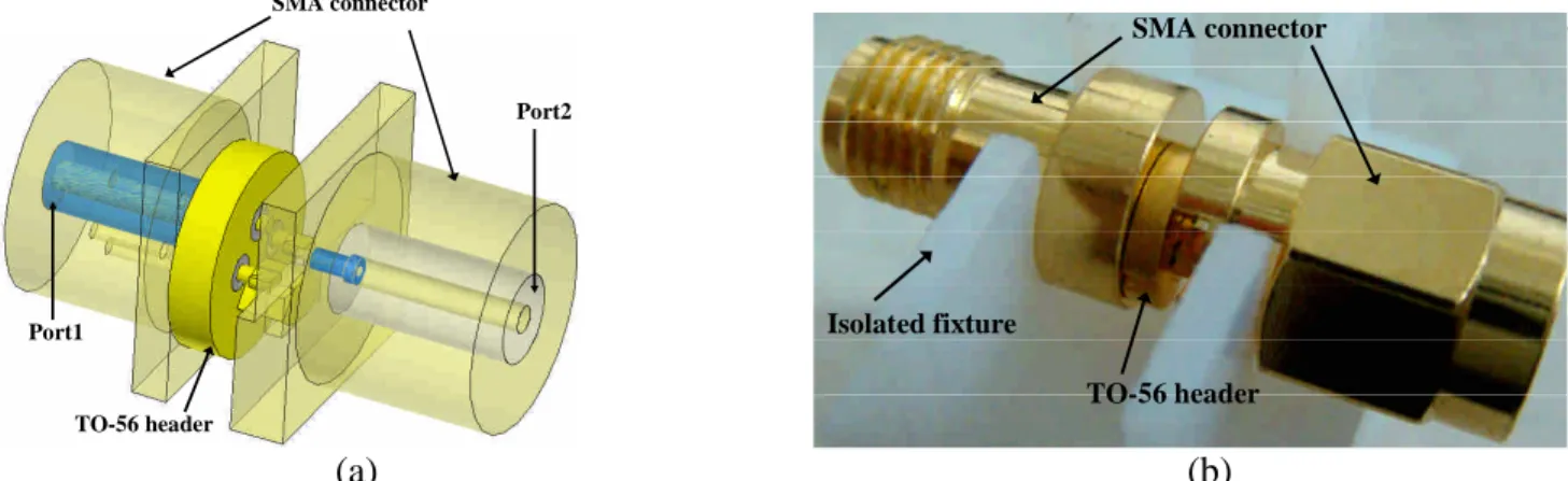
To verify the applicability of the HFSS simulation, a special experiment has been designed. A pair of unique SMA connectors with a characteristic impedance of 50 Ω is designed and fabricated. The SMA connectors can probe a feed lead of the TO-56 header directly and connect to a vector network analyzer (VNA) to measure the high frequency characteristics without an extra evaluation board [10]. We constructed a 3D electromagnetic model including a TO-56 header and SMA connectors, to calculate the high frequency characteristics through HFSS simulation. A schematic drawing of the TO-56 header and SMA connectors is shown in Fig. 1(a). The feed lead at the right hand side of TO-56 header is directly probed. The ground contact is made by touching the base and stem of TO-56 header. The base and stem of TO-56 header contact with the ground of the SMA connectors. The diameter of the TO-56 header is 5.6 mm; the diameters of the feed lead and feedthrough hole are 0.45 and 1 mm, respectively [10]. The surfaces of the header and the feed lead are plated with a 1 μm thick of gold film and the current waves flow through the surface at high
frequency. In this study, we only consider gold, as it is the most conductive metal [23]. The parameters of gold are selected as: a relative permittivity (εr) of 1; a relative permeability (μr) of 0.99996; and electric
conductivity (σ) of 4.1x10⁷S/m. All the dimensions and related materials come from specifications provided by the vendor. The realistic photograph is shown in Fig.1(b). An isolated fixture is inserted to hold the SMA connectors and the TO-56 header firmly, to obtain the best electrical contact.
SMA connector TO-56 header Port1 Port2 SMA connector TO-56 header Isolated fixture (a) (b)
Fig. 1. The configuration of a TO-56 header and the SMA connectors, (a) the schematic drawing and (b) the photograph.
An Agilent 8722ES VNA is calibrated to two cable test ports using a full two port calibration procedure. The port 1 and port 2 of the fixture are connected the cable test ports of VNA to measure S11 and S21 in the frequency range up to 20 GHz. The simulated and measured results of S11 coincide well, and are shown in Fig. 2(a). The S11 of the TO-56 header associated with the SMA connectors is less than -10 dB at 7 GHz. No evident resonance point is measured, indicating that the measurement setup does not induce any improper circuit elements or electrical connections. The reflection loss increases to over -10 dB at higher frequency operation due to the impedance mismatch of the TO-56 header. The simulated and measured results of S21 are shown in Fig. 2(b). The above 0dB offset of S21 is induced by a limited calibration capability. The 3-dB transmission bandwidth reaches 17 GHz. In this case, the TO-56 header is connected by a perfect transmission line with a characteristic impedance of 50 Ω. The parasitic effect, induced by bonding wires, is excluded. When associated with a laser diode and bonding wires, the 3-dB transmission bandwidth can only deteriorate. Obviously, the TO-56 header can not be applied in the coming 20GFC and 100GbE networks. Furthermore, the simulated result shows good agreement with the experimental result in the frequency range up to 20 GHz. The accuracy of the constructed 3D electromagnetic model using HFSS simulation software is proven.
0 2 4 6 8 10 12 14 16 18 20 -30 -25 -20 -15 -10 -5 0 R ef le ct io n lo ss [S 1 1 ] (d B ) Frequency (GHz) Simulation (HFSS) Measured 0 2 4 6 8 10 12 14 16 18 20 -8 -7 -6 -5 -4 -3 -2 -1 0 1 Simulation (HFSS) Measued In se rt io n lo ss [S 2 1 ] (d B ) Frequency (GHz) (a) (b)
Fig. 2. The simulated and measured of (a) the S11 and (b) the S21 curves for a TO-56 header with the SMA connectors.
III. DESIGN ANDPROPOSAL OF THENEWTO-CANHEADER
A. Impedance analysis of the feed lead of TO-Can header
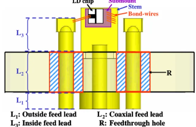
feed lead transmitted high frequency signal can be divided into three parts: outside (L1); coaxial (L2); and inside (L3). The feedthrough hole (R) is filled with a sealed glass to insulate the coaxial feed lead and TO-Can header. The relative dielectric constant (εr) of the sealed glass in the feedthrough holes can range from 4.1 to
5.5. For a single ended, directly modulated laser application, the signal feeds from the outside feed lead to the inside feed lead, and returns to the ground through the stem and the ground pin of the TO-56 header.
L3 L1 L2 Bond-wires Stem LD chip Submount
L1: Outside feed lead L2: Coaxial feed lead
L3: Inside feed lead R: Feedthrough hole
R L3 L1 L2 Bond-wires Stem LD chip Submount
L1: Outside feed lead L2: Coaxial feed lead
L3: Inside feed lead R: Feedthrough hole
R
Fig. 3. The schematic drawing of the conventional coaxial laser package with a TO-56 header.
1) Outside feed lead
A longer feed lead induces a larger parasitic inductance; giving the feed lead a large inductance limits the transmission bandwidth. To ensure the maximum transmission bandwidth, the length of outside feed lead should be designed as short as possible. From the specification of the TO-56 header, and the length of outside feed lead is assumed to be 0.5 mm, the parasitic inductance is 0.1142 nH.
2) Coaxial feed lead
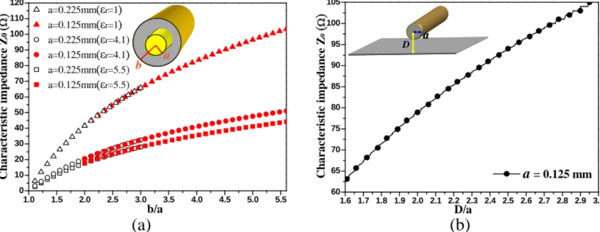
The coaxial feed lead and the feedthrough hole form a coaxial line [24], [27]. For a conventional TO-56 header, the diameter of feed lead (a) is 0.225 mm, the diameter of feedthrough hole (b) is 0.5 mm, and εris 5.5. The theoretical Z0is20 Ω,which doesnotmatch thestandard 50 Ω requirement.Therefore,wemustdevisea way to increase the characteristic impedance of this part to match the impedances of the outside feed lead and the laser driving circuit. Z0can be increased by increasing the radius of the feedthrough hole, decreasing the radius of the feed line, or decreasing the relative dielectric constant of the sealed glass. To preserve good hermetic performance of a TO-Can header, the sealed glass is limited to a few options. The lowest relative dielectric constant of commercially available sealed glass is 4.1. For practical manufacturing, the minimum inner radius of the feed lead is limited to 0.125 mm; due to the tight space requirements of the TO-Can header, the radius of the feedthrough hole is limited to 0.7 mm. In other words, the maximum b/a ratios are 3.1 and 5.6 for feed lead radii of 0.225 and 0.125 mm, respectively. Combining all the practical issues and constraints determines the relation between Z0 and the related parameters shown in Fig. 4(a). The maximum Z0of a feed lead with aradiusof0.225 mm is33 Ω;therelativedielectric constantofthesealed glassis4.1,and theb/a
ratio is 3.1, shown as circles and squares in the figure. If the radius of the feed lead is reduced to 0.125 mm, then the maximum Z0isincreased to 50 Ω;the relativedielectricconstantofthesealed glassis4.1 and theb/a ratio is 5.6, indicated by solid dots in the figure. When the relative dielectric constant decreases to 1, Z0can be adjusted through an impedance range of 20 to 100 Ωas shown in the figure as triangles and solid triangles. This kind of air gap design should co-locate with the sealed glass in a practical application. Inserting a highly adjustable impedance section in the feed lead allows optimization of the impedance of the TO-Can header.
3) Inside feed lead
The inside feed lead of the TO-56 header is not designed with a transmission line model. The signal passes through the inside feed lead over the stem without an adequate flat ground plane in the TO-56 header. To enable a higher transmission bandwidth, the inside feed lead must be designed according to a transmission line model; the proposed design introduces a wire over ground concept to increase the transmission bandwidth. The transmission line of a wire over ground plane can be derived from a two wire model [24], [27]. D is the distance of the inside feed lead (wire) and the stem (ground plane), and a is the radius of the inside feed lead. Z0is a hyperbolic cosine function of D/a, and the relation between Z0and D/a is shown in Fig. 4(b).
a b a b 1.0 1.5 2.0 2.5 3.0 3.5 4.0 4.5 5.0 5.5 0 10 20 30 40 50 60 70 80 90 100 110 120 C h a r a ct er is ti c im p ed a n c e Z 0 ( ) b/a a=0.225mm(εr=1) a=0.125mm(εr=1) a=0.225mm(εr=4.1) a=0.125mm(εr=4.1) a=0.225mm(εr=5.5) a=0.125mm(εr=5.5) 1.6 1.7 1.8 1.9 2.0 2.1 2.2 2.3 2.4 2.5 2.6 2.7 2.8 2.9 3.0 60 65 70 75 80 85 90 95 100 105 a= 0.125 mm C h a ra ct er is ti c im p ed a n ce Z 0 ( ) D/a D a D a (a) (b)
Fig. 4. The relation of Z0and related parameters of (a) the coaxial feed lead and (b) the inside feed lead.
B. Proposed new design for a TO-Can header
From our discussions, the new TO-Can header adopts the transmission line concept and meets practical manufacturing concerns. Figure 5 shows the structure of the TO-Can header in a 3D configuration and cross sectional view. Pins 1 and 3 are feed leads for the input signal path; pin 2 is for a monitor diode output, and pins 4 and 5 are grounding feed leads for the signal return path. The diameter and thickness of the TO-Can header are 5.6 and 0.9 mm, respectively. This TO-Can header has a similar configuration and dimensions to the TO-56 header. The manufacturing processes and equipment are compatible.
The radius of the feed lead is chosen as 0.125 mm. For the coaxial feed lead, a two section feedthrough hole of different diameters is designed to minimize the impedance discontinuity and balance the overall impedance. The first section (feedthrough hole 1) has a diameter of 0.96 mm and is filled with sealed glass (εs= 4.1); this
section is0.6 mm long.Thecharacteristicimpedanceofthefirstsection is40 Ω.A 50 Ω coaxialfeed lead needs a larger feed through hole and a TO-Can header with a normal size cannot accommodate that. To overcome the smaller impedance of the first section, a second section (feedthrough hole 2) is added to balance the characteristic impedance. The second section has a diameter of 0.58 mm, a length of 0.3 mm, and an air gap to insulate the feed lead from the header. The impedance of the second section is around 50 Ω. This also provides more freedom to adjust the distance between the inside feed lead and the stem due; a small hollow hole must be considered in the production molding process. Because the load impedance might differ in various applications, this two section coaxial feed lead design is an optimized result.
To construct a transmission line configuration, this new TO-Can header has a wide stem to maintain the wire over ground transmission of the inside feed lead. The distance between the inside feed lead and the stem is the key parameter for adjusting the characteristic impedance. The radius of the feed lead is 0.125 mm. The distance between the center of the feed lead and the stem is 0.29 mm. The impedance of the inside feed lead (wire-over-ground) is 76 Ωwhich is a compromised result between realization and performance. Inside of the TO-Can header, a LD chip with a submount is bonded on the center of the stem. To shorten the length of the bonding wire between the inside feed lead and the LD chip, the inside feed lead is bent with a right angle and then lengthened by one small section of 0.5 mm.
Stem Base Feed lead Feedthrough hole 1 Feedthrough hole 2 1 3 2 4 5 D Feedthrough hole 1(sealed glass)
Feedthrough hole 2(air)
(a) (b)
IV. DEMONSTRATION OFFREQUENCYCHARACTERISTICS OFTHENEWTO-CANHEADER ANDPACKAGE
A. Frequency characteristics of the new TO-Can header
The electrical characteristics of the new TO-Can header are simulated and analyzed with HFSS. Both the new TO-Can header and the conventional TO-56 header aresimulated with aterminalimpedanceof50 Ω atboth input and output ports of the feed lead. The S11 simulated results and comparison are shown in Fig. 6(a). The reflection loss of the new design is held below -10 dB at under 26 GHz. The S21 simulated results and comparison are shown in Fig. 6(b). The 3-dB transmission bandwidth of the TO-56 header reaches 17 GHz while the 3-dB transmission bandwidth of the new TO-Can header is more than 40 GHz. The phases and group delay of S21 are shown in Fig. 6(c) and 6(d), respectively. The linearity of the new design is better than that of the conventional TO-56 header in the operational range of interest.
0 5 10 15 20 25 30 35 40 -50 -45 -40 -35 -30 -25 -20 -15 -10 -5 0
New TO-can header TO-56 header R ef le ct io n lo ss [S 1 1 ] (d B ) Frequency (GHz) 0 5 10 15 20 25 30 35 40 -8 -7 -6 -5 -4 -3 -2 -1 0
New TO-can header TO-56 header In se r si o n lo ss [S 2 1 ] (d B ) Frequency (GHz) 0 5 10 15 20 25 30 35 40 -250 -200 -150 -100 -50 0 50 100 150 200 250
New TO-can header TO-56 header P h a se [S 2 1 ] (d eg ) Frequency (GHz) 0 5 10 15 20 25 30 35 40 0 2 4 6 8 10 12 14 16 18 20
New TO-can header TO-56 header Frequency (GHz) G ro u p d el a y [S 2 1 ] (p se c) (a) (b) (c) (d)
Fig. 6. The simulation results of the new TO-Can and the conventional TO-56 header with an impedance terminal of 50 Ω.(a) S11, (b) S21, (c) the phase curves, and (d) the group delay of the S21.
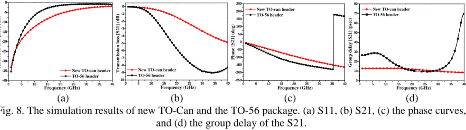
B. Frequency characteristics of the new TO-Can header with bonding wires
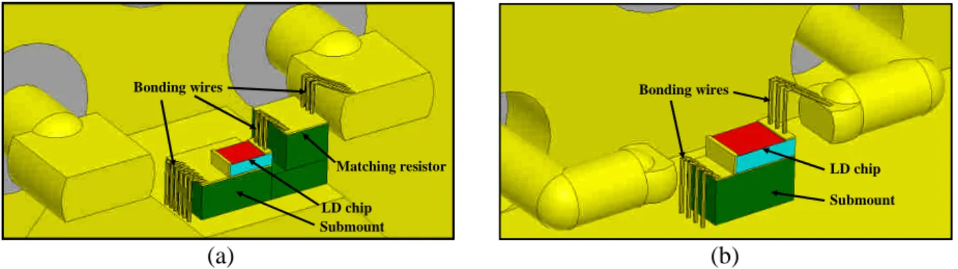
Figure 7(a) shows a typical layout inside the coaxial TO-56 laser package for single ended design, which consists of a matching resistor, LD chip, and submount on the stem [10]. The submount is made of aluminum nitride (AlN). A set of gold wires connects the feed lead, the matching resistor, and the LD chip. The bottom of the LD chip is soldered on the submount. Since the submount is insulated, gold wires are bonded to connect the surface electrode of the submount and the stem of the TO-56 header. The signal feeds into the LD chip through the feed lead and returns to ground through the stem of the TO-56 header. The layout of the new package is similar to the TO-56 package, and is shown in Fig. 7(b). Because the distance between the feed lead and LD chip is short, wires can be bonded wire directly without inducing serious parasitic inductance. 3D electromagnetic models for the layout of new TO-Can and TO-56 packages have been constructed with the HFSS software, using their layouts and inputs, to simulate the high frequency characteristics. To identify the influence of bonding wires on the structure, an ideal case is assumed. The LD chip is assumed as a load of 50 Ω,and thematching resistorisassumed to beaperfectconductor.The diameter and the length of the bonding wire are set at 0.8 mil and 0.3 to 0.5 mm, respectively. The setting of bonding wires is similar to a realistic condition. Submount LD chip Matching resistor Bonding wires Submount LD chip Matching resistor Bonding wires Submount LD chip Bonding wires Submount LD chip Bonding wires (a) (b)
Fig. 7. The layout of TO-Can package of (a) TO-56 header and (b) new TO-Can header.
The S11 simulated results are shown in Fig. 8(a). For the new package, S11 is held below -10 dB for up to 14 GHz and the TO-56 package is 7 GHz. In the S21 simulated results, shown in Fig. 8(b), the 3-dB transmission bandwidth of the TO-56 package is 14 GHz which is a 3 GHz deterioration compared with the intrinsic TO-56 header. The 3-dB transmission bandwidth of the new TO-Can package is over 28 GHz. The phase curves and group delay of S21 for the new TO-Can package and the conventional TO-56 package are shown in Fig. 8(c)
and 8(d), respectively. The linear region of the new TO-Can package is clearly superior to that of the conventional TO-56 package in the operating range of interest.
In addition, by adopting the ADS software to fit the HFSS simulated S11, S21, and phase curves and extracting the electrical characteristics of each lumped element, equivalent circuits are established for both the intrinsic TO-Can header and new TO-Can package. Comparing the two equivalent circuits gives the inductance contributed by bonding wires. The calculated parasitic inductance of the bonding wires connecting the feed lead and LD chip is about 0.3 nH. This is similar to the value in a previously paper [10], [28].
0 5 10 15 20 25 30 35 40 -40 -35 -30 -25 -20 -15 -10 -5 0
New TO-can header TO-56 header Frequency (GHz) R ef le ct io n lo ss [S 1 1 ] (d B ) 0 5 10 15 20 25 30 35 40 -10 -9 -8 -7 -6 -5 -4 -3 -2 -1 0
New TO-can header TO-56 header T r a n sm is si o n lo ss [S 2 1 ] (d B ) Frequency (GHz) 0 5 10 15 20 25 30 35 40 -250 -200 -150 -100 -50 0 50 100 150 200 250
New TO-can header TO-56 header P h a se [S 2 1 ] (d e g ) Frequency (GHz) 0 5 10 15 20 25 30 35 40 0 10 20 30 40 50 60 70 80
New TO-can header TO-56 header G ro u p d el a y [S 2 1 ] (p se c) Frequency (GHz) (a) (b) (c) (d)
Fig. 8. The simulation results of new TO-Can and the TO-56 package. (a) S11, (b) S21, (c) the phase curves, and (d) the group delay of the S21.
V. ANALYSIS OF THETO-CANLASERMODULE WITH A24.5 GHZDFB-LD EQUIVALENTCIRCUIT
A complete coaxial laser module analysis should take the characteristics of the DFB-LD into consideration; however, it is difficult to model the DFB-LD with HFSS software. Therefore, ADS software is adopted to simulate the high frequency characteristics through an equivalent circuit model. By referring to the equivalent circuit of DFB-LD from a previous study [10] and reducing the diffusion capacitance, the space charge capacitance, and the parasitic capacitance, a modified equivalent circuit of DFB-LD is established. The diffusion capacitance, the space charge capacitance, and the parasitic capacitance of the modified equivalent circuit of DFB-LD are 25pF, 2pF, and 0.15pF, respectively. The 3-dB transmission bandwidth of the modified model is up to 24.5 GHz. The S21 of the original and modified DFB-LD models are shown in Fig. 9(a). By using a time domain simulator, 25 Gbit/s eye diagrams are simulated and shown in insets of Fig. 9(a). The two equivalent circuits for the DFB-LD are combined with the extracted equivalent circuits of the TO-56 package and the new TO-Can package to simulate the high frequency characteristics of a coaxial laser module with ADS software. The simulated S21 results of the coaxial laser module are shown in Fig. 9(b). The 3-dB transmission bandwidth of the module that adopts the new TO-Can package reaches 15.5 and 20.5 GHz with the original and the modified DFB-LD models, respectively. The 25 Gbit/s eye diagrams of the module are simulated and shown in insets of Fig. 9(b). Packaging the module with a better DFB-LD can further improve the 3-dB transmission bandwidth. The 3-dB transmission bandwidth of the module packaged with the TO-56 header is around 11 GHz for either the original or modified DFB-LD models. The comparison between the new TO-Can module and TO-56 module shows a significant improvement in the 3-dB transmission bandwidth. 0 5 10 15 20 25 30 35 40 -25 -20 -15 -10 -5 0 5 Original LD model Modified LD model Frequency (GHz) F re q u en cy R es p o n se [S 2 1 ] (d B ) 0 5 10 15 20 25 30 35 40 -25 -20 -15 -10 -5 0 5 Original LD model Modified LD model Frequency (GHz) F re q u en cy R es p o n se [S 2 1 ] (d B ) 0 5 10 15 20 25 30 35 40 -40 -35 -30 -25 -20 -15 -10 -5 0 5
New TO-can + Modified LD model New TO-can + Original LD model TO-56 + Modified LD model TO-56 + Original LD model
Frequency (GHz) F re q u en cy R es p o n se [S 2 1 ] (d B ) 0 5 10 15 20 25 30 35 40 -40 -35 -30 -25 -20 -15 -10 -5 0 5
New TO-can + Modified LD model New TO-can + Original LD model TO-56 + Modified LD model TO-56 + Original LD model
Frequency (GHz) F re q u en cy R es p o n se [S 2 1 ] (d B )
equivalent circuit model, (b) Simulated frequency responses and 25 Gbit/s eye diagrams of coaxial laser module.
VI. CONCLUSION
A new TO-Can header for 25 Gbit/s transmission and low cost coaxial laser modules has been proposed and demonstrated. The new TO-Can header adopts a two section feedthrough hole and a wire over ground inside feed lead and is designed with practical manufacturing considerations in mind. The applicability of the simulation tool was verified with a novel experiment. The high frequency characteristics of the new TO-Can header show significant improvements compared with the conventional TO-56 header. The reflection loss is less than –10 dB below 26 GHz, and the 3-dB transmission bandwidth exceeds 40 GHz with an ideal 50 Ω
terminal. Taking practical bonding wires into consideration, the 3-dB transmission bandwidth deteriorates to 28 GHz. After extracting the equivalent circuit of the new TO-Can package and combining it with a 24.5 GHz DFB-LD, the coaxial laser module achieves a 3-dB modulation bandwidth of 20.5 GHz, which can be operated at 25 Gbit/s transmissions. In summary, a significant improvement of 3-dB transmission bandwidth of a new TO-Can module has been proposed and demonstrated to provide a low cost solution for high bit rate coaxial laser module. It can be applied in the emerging 20GFC and four channel WDM 100GbE networks, and will serve the next generation of optical access networks.
REFERENCES
[1] Fibre Channel Industry Association (FCIA) [Online]. Available: http://www.fibrechannel.org/. [2] HSSG Tutorial [Online]. Available: http://www.ieee802.org/3/hssg/public/nov07/index.htm.
[3] C. Cole, D. Allouche, F. Flens, B. Huebner, and T. Nguyen,“100GbE-opticalLAN technologies,” IEEE
Commun. Mag., vol. 45, no. 12, pp. 12–19, Dec. 2007.
[4] S. Matsuo, T. Kakitsuka, T. Segawa, R. Sato, Y. Shibata, R. Takahashi, H. Oohashi, and H. Yasaka et al., “4 x 25 Gb/sFrequency-Modulated DBR Laser Array for 100-GbE 40-km Reach Application,”IEEE
Photon. Technol. Lett., vol. 20, no. 17, pp. 1494–1496, Sep. 2008.
[5] A. Ebberg, F.Auracher, and B. Borchert, “10 Gbit/s transmission using directly modulated uncooled MQW ridgewaveguide DFB lasersin TO package,”Electron.Lett.,vol.36,no.17,pp.1476–1477, Aug. 2000.
[6] K. Sakai, H. Aruga, S.-I. Takagi, M. Kawano, M. Negishi, Y. Kondoh, and S.-I. Kaneko, “1.3-μm uncooled DFB laser-diode module with a coupled differential feed for 10-Gb/sEthernetapplications,”J. Lightwave Technol., vol. 22, no. 2, pp. 574–581, Feb. 2004.
[7] Lewis B. Aronson, Giorgio Giaretta, Stefano Schiaffino, and Beck Mason, “Transmitter optical subassembly forXFP applications,”in Proc.ofECTC’2005,vol.1,2005,pp.1058–1062.
[8] D. Kim, J. Shim, Y.-C.Keh,and M.Park,“Design and Fabrication ofaTransmitterOpticalSubassembly (TOSA) in 10-Gb/s Small-Form-Factor Pluggable (XFP) Transceiver,” IEEE J. Select. Top. Quant. Electron., vol. 12, no. 4, pp. 776–782, July/Aug. 2006.
[9] J.Lee,S.Nam,S.H.Lee,and J.Jeong,“A completesmall-signal equivalent circuit model of cooled butterfly-type2.5 GbpsDFB lasermodulesand itsapplication to improve high frequency characteristics,” IEEE Trans. Adv. Packag., vol. 25, no. 4, pp. 543–548, Nov. 2002.
[10] T.-T. Shih, M.-C. Lin, and W.-H.Cheng,“High-Performance Low-Cost 10-Gb/s Coaxial DFB Laser Module Packaging by Conventional TO-Can Materials and Processes,” IEEE J. Select. Top. Quant. Electron., vol. 12, no. 5, pp. 1009–1015, Sep/Oct. 2006.
[11] Pei-Hao Tseng, Tien-Tsorng Shih, Hao-Wei Chen, Yaw-Dong Wu, and Wood-Hi Cheng, “Electrical Packaging Characteristics of a 25-Gbit/s Low-CostCoaxialLaserModule,”in Proc.ofOECC2010,July 2010, pp. 56-57.
[12] P. A. Morton, T. Tanbun-Ek, R. A. Logan, N. Chand, K.W. Wecht, A.M. Sergent, and P.F. Sciortino, “Packaged 1.55 μm DFB laserwith 25 GHz modulation bandwidth,”Electron.Lett.,vol.30,no.24,pp. 2044–2046, 1994.
[13] F. Steinhagen, H. Hillmer, R. Losch, W. Schlapp, H. Walter, R. Gobel, E. Kuphal, H.L. Hartnagel, and H. Burkhard,“AIGalnAs/lnP 1.5μm MOW DFB laserdiodesexceeding 20GHz bandwidth,”Electron.Lett., vol. 31, no. 4, pp. 274–275, Feb. 1995.
[14] S. Lindgren, H. Ahlfeldt, L. Backlin, L. Forssen, C. Vieider, H. Elderstig, M. Svensson, L. Granlund, L. Andersson, B. Kerzar, B. Broberg, O. Kjebon, R. Schatz, E. Forzelius, and S. Nilsson, “24-GHz modulation bandwidth and passive alignment of flip-chip mounted DFB laser diodes,” IEEE Photon. Technol., Lett., vol. 9, no. 3, pp. 306–308, Mar. 1997.
[15] Yasuhiro Matsui,HitoshiMurai,Shin Arahira,Satoko Kutsuzawa,and Yoh Ogawa,“30-GHz bandwidth 1.55-μm strain-compensated InGaAlAs-InGaAsP MQW laser,”IEEE Photon.Technol.,Lett.,vol.9,no.1, pp. 25–27, Jan. 1997.
[16] K. Otsubo, M. Matsuda, K. Takada, S. Okumura, M. Ekawa, H. Tanaka, S. Ide, K. Mori and T. Yamamoto, “Uncooled 25 Gbit/s direct modulation of semi-insulating buried-heterostructure 1.3 μm AlGaInAs quantum-wellDFB lasers,”Electron.Lett.,vol.44,no.10,pp.631–632, May, 2008.
[17] K. Nakahara, T. Tsuchiya, T. Kitatani, K. Shinoda, T. Taniguchi, T. Kikawa, M. Aoki, and M. Mukaikubo, “40-Gb/s Direct Modulation With High Extinction Ratio Operation of 1.3-μm InGaAlAsMultiquantum WellRidgeWaveguideDistributed Feedback Lasers,”IEEE Photon.Technol.,Lett.,vol.19,no.19,pp. 1436–1438, Oct. 2007.
[18] R. Paoletti, Member, IEEE, M. Agresti, D. Bertone, C. Bruschi, S. Codato, C. Coriasso, R. Defranceschi, P. Dellacasa, M. Diloreto, R. Y. Fang, P. Gotta, G. Meneghini, C. Rigo, E. Riva, G.Roggero, A. Stano, M. Meliga,“Uncooled 20 Gb/sdirectmodulation ofhigh yield,highly reliable1300 nm InGaAlAsridge DFB lasers,”in Proc.ofOFC’2009,Mar.2009,pp.1–3, OThT1.
[19] Ashish K.Verma,MichaelSteib,Yuk Lung Ha,TsurugiSudo,“25Gbps1.3μm DFB laserfor10–25km transmission in 100GBE systems,”in Proc.ofOFC’2009,Mar.2009,pp.1–3, OThT2.
[20] T. Tadokoro, T. Yamanaka,F.Kano,H.Oohashi,Y.Kondo,and K.Kishi,“Operation ofa25-Gbps direct modulation ridge waveguide MQW-DFB Laserup to 85 °C,”in Proc.ofOFC’2009,Mar.2009,pp.1–3, OThT3.
[21] K. Otsubo, M. Matsuda, S. Okumura, A. Uetake, M. Ekawa, and T. Yamamoto, “Low-driving-current high-speed direct modulation up to 40 Gb/s using 1.3-μm semi-insulating buried-heterostructure AlGaInAs-MQW distributed reflector(DR)lasers,”in Proc.ofOFC’2009,Mar.2009,pp.1–3, OThT6. [22] K. Otsubo, M. Matsuda, K. Takada, S. Okumura, M. Ekawa, H. Tanaka, S. Ide, K. Mori, and T.
Yamamoto, “1.3-μm AlGaInAs Multiple-Quantum-Well Semi-insulating Buried-Heterostructure Distributed-Feedback Lasers for High-Speed DirectModulation,”IEEE J.Select.Top.Quant.Electron., vol. 15, no. 3, pp. 687–692, May/July 2009.
[23] D. K. Cheng, Field and wave electromagnetics 2nd, Addison Wesley Longman, 1989.
[24] H. Nakano, S. Sasaki, M. Maeda, and K. Aiki, “Dual-In-Line Laser Diode Module for Fiber-Optic Transmission Up to 4 Gbit/s,”IEEE J.LightwaveTechnol., vol. LT-5, no. 10, pp. 1403-1411, Oct. 1987. [25] Frederick W. Grover, Inductance Calculations, Dover Phoenix Editions, 2004.
[26] T. Ban, Y. Lee, S. Makino, H. Hayashi, H. Toyoda, M. Shishikura, T.Sugawara, S. Tanaka, S. Tsuji, and M. Aoki, M. Sasada, H. Takamatsu,H.Yamamoto,and M.Okayasu,“25-Gbps Receiver for 100-Gbps Ethernet employing Cost-effectiveSmallCoaxialPackage,”in Proc.ofECOC’2008,pp.We1C6.
[27] D. M. Pozar, Microwave Engineering 3rd, John Wiley & Sons, 2004.
[28] C. Chen, N. H. Zhu, S. Jian Zhang, and Y. Liu, “Characterization of Parasitics in TO-Packaged High-Speed LaserModules,”IEEE Trans.Adv.Packag.,vol.30,no.1,pp.97-103, Feb. 2007.
國科會補助專題研究計畫項下出席國際學術會議心得報告
日期: 100 年 10 月 30 日
一、參加會議經過
前往參加歐洲光網路與光通信研討會(European Conference on Net Works and Optical and Optical Communication 簡稱 NOC),今年與光纖網路及基礎架構研討會(Conference on Optical Cabling and Infrastructure 簡稱 OC&I)合辦,今年舉辦於英國新堡(Newcastle upon)的諾桑比亞大學(Northnmbria University),至今以是第 16 屆事逢 2011 年故稱為 NOC2011,主辦學校諾桑比亞大學前身創建於 1870 年,1969 年與其他院校合併再 1992 年升格大學,該校歷史悠久,研討會主辦單位有 NOC Continuity Fund and Harmer Associates 及 Northnmbria University 主 辦 , IEEE 通 信 協 會 英 國 分 會 (IEEE UK-RI Communications Chapter)及 IEEE UK&RISection…..等贊助協辦,NOC 為歐洲地區頗具權威的研討會, 本次研討會主席為 Professor Zabih Ghassemlooy,研討會主要以光網路與光通信為主,內容包含頻帶嵌 入技術(Broadband Access Technologies) ,光傳輸網路(transport and photonic networks),節能電信網路 (Energy Saving in telecommunications Networks),光纖到家與傳輸環境(Optical networks at Home and in Transportation Environments) , 區 域 網 路 (Metropolitan Networks) , ( 零 組 件 技 術 開 發 )Advances in Component Technology,Future directions for QoS Circuit and Packet Switched Networks 等主題。
本研究室主要研究內容為低成本光電構裝,量測,光電應用等研究,且長期研究通訊雷射發光元件構 裝與量測及同軸構裝基座 3D 模擬,建構研究相關製程與高頻量測設備,故指派參與研討會,目的為了 解各研究領域現況與發展,充實研究室研究方向相關知識積極與國際接軌。 研討會註冊從 7 月 20 日早上 9:00 開始開始並有一場簡單之歡迎會。正式的研討會則在 8 月 29 日週一 早上 9:00 開始,由大會主席致歡迎詞,三天的議程安排緊湊,每日早上 9:00 開始,先安排幾位 Keynote speaker 作專題演講後,每日會議至下午 6:00 結束,研討會於 7 月 22 日 14:30 結束,研討會中邀請各
計畫編號
NSC 99-2221-E-151-045-
計畫名稱
同軸式雷射二極體模組的三維電磁模型與射頻特性分析
出國人員
姓名
余志偉
服務機構
及職稱
國立高雄應用科技大學電子工
程系博士班研究生
會議時間
100 年 7 月 20 日至
100 年 7 月 22 日
會議地點
Northnmbria University Newcastle upon Tyne, UK
會議名稱
(中文)第十六屆歐洲網路與光通訊會議
(英文)
16thEuropean Conference on Net Works and Optical Communications發表論文
題目
(中文)無
(英文)
領域的前輩與先進作專題演講,受邀的演講嘉賓有任教於香港理工大學 Professor Lu Chao、愛丁堡大 學 Professor Harald Haas 、Dr. Roberto Llorente、Professor Richard V. Penty、Dr.-lig.Dominic A. Schupke、 Professor Harm J.S.Dorren 等六位學者,分別與各研討會前專題演講,三天研討會主要內容為 Broadband access technologies 、 Components and physical issues of optical networks 、 Energy saving in telecommunication networks、QoS and management in Optical networks、Optical Communications-General、 Transport and photonic networks…..等六大主題。
第二天早上所發表的主題 60GHZ Intermediate Frequency over Fiber Using a Passive Multipoint To Multipoint Architecture,內容為 60GHZ 的訊號利用 Radio-Over-Fiber(ROF)做點對點傳輸架構,使用低 成本光電元件,再兩個商業用的 Wireless HD 的傳輸設備實現 3Gbit/s 傳輸速度,如下圖(1)所示為單一 光電轉換電路,電路包含光收發與微波無線訊號收發等功能,圖(2)為此模主的自發自收量測架構。近 年來網路傳輸頻寬提升,資料量大速度快,且移動通訊設備需要的無線上網頻寬也越來越大,使用無 線通訊上網的機會也越來越多元,所以由實體的光網路傳輸量大的優點,作為遠距離的高速傳輸,連 結既有的微波通訊架構,提升行動無線網路頻寬。
圖(1)Intermediate Frequency over Fiber Transducer (TRoF)
圖(2)Back-to-back and RoF setup at IF (5 GHz)
第 三 天 的 受 邀 演 講 嘉 賓 所 演 說 的 主 題 是 :Triple-Play and 60-Ghz Radio-Over-Fiber Techniques for Next-Generation Optical Access Networks,都是光纖傳輸架構上的變化,利用多個不同的無線傳輸設備 之間利用光纖傳輸光電訊號,利用光纖傳輸加速無線媒體間的傳輸。
編號 BATIII-2 題目為 Cost effective RoF with VCSELS and Multimode Fiber 中提到利用垂直共振腔結構 的 VCSELS 雷射及多模光纖(MMF)結構,經模擬及實作後驗證其低成本的 RoF 結構是否可以實現,架 構如圖(3)
圖(3)Up-and down converted RoF system
在Investigation of Optical Millimeter-Wave and Heterodyne Techniques in Radio-over-Fiber Systems 文 中,(ROF)以建議作為替代毫米波(MMV)擴展在微波通訊(RF)頻率範圍的無線電頻率,但最大的挑戰是 降低光纖衰減與色散問題對信號源與(ISI)產生影響,對於信號有兩個調製方案,(BPSK)與(QPSK)兩 種,建議是用連續雷射光(CW)在30GHZ傳輸在BPSK和QPSK信號載波中。 使用60GHZ與30GHZ的載波相比較下,結果為30GHZ的BPSK和QPSK的電信號可改善傳輸距離達20公 里,BPSK與QPSK等調變信號方式在BER為10^-5g時信號雜訊比(SNR)為分別為BPSK的11db與18db以 及QPSK的16db與26db,圖(4)為ROF示意圖,表示Wireless RF MMW 波型訊號使用微波方式傳輸給有 線的光纖傳輸架構,經由MZM調變接收微波信號後轉換成光訊號傳輸,光訊號透過MMW-RoF的光纖 纜線傳輸到電信機房,圖(5)為系統量測架構以自發自收方式量測誤碼率。
圖(4)Comparing MMW in RF and RoF. LD: Laser diode, MZM: Mach-Zehnder Modulator, Electrical link: Optical link:
圖(5)A block diagram of 60 GHz MMW system. LD: laser diode; SD-MZM: single drive Mach-Zehnder modulator; DD-MZM: dual drive Mach-Mach-Zehnder modulator; PD: Photo detector.
二、與會心得與建議 此次感謝國科會計畫經費,讓我有幸前往英國諾桑比亞大學參與 NOC2011 研討會,研討會中處處 都感受的到主辦單位的用心,與英國人的紳士風度,研套會中能了解世界各國不同實驗室對光電 通訊領域的貢獻與各實驗方向,有機會與不同實驗室的研究先進交流,研討會中邀請的專題研討 嘉賓,也在每一場次的開頭,點出了未來光電通訊領域的重點發展方向值得深入了解,及光電通 訊未來的應用與研究,其中也了解到各研究人員對研究領域與研究價購量測的嚴謹,會後參觀諾 桑比亞大學的上課及實習空間設備,大學城中新舊建築都在在顯示大學的活力,激發出學生的創 新靈感,本次參訪收穫不僅僅事知識還有多西方文化更進一步的了解,獲益良多。 三、攜回資料名稱及內容 研討會論文集光碟片一片及相關文宣品 會場外與研討會指標合影及會議舉行地點(工科大樓)照片
第二天的演講嘉賓香港理工大學 Professor Lu Chao
會場大廳
國科會補助計畫衍生研發成果推廣資料表
日期:2011/10/31國科會補助計畫
計畫名稱: 同軸式雷射二極體模組的三維電磁模型與射頻特性分析 計畫主持人: 施天從 計畫編號: 99-2221-E-151-045- 學門領域: 光纖通訊與波導光學研發成果名稱
(中文) 雷射二極體模組的三維電磁模型建置與射頻特性分析技術(英文) The 3D electromagnetic model and RF characterization technique of a laser diode module
成果歸屬機構
國立高雄應用科技大學發明人
(創作人)
施天從技術說明
(中文) 未來高速率的光纖網路的傳輸系統,均需要單一通道傳輸速率為25-Gb/s或以上 的雷射光源。現在可以符合該傳輸速率需求的雷射光源的封裝結構以價格昂貴的 蝶式封裝為主,因此在大量普及的應用上有所困難,所以開發傳輸速率達25-Gb/s的低成本的同軸式TO-CAN雷射封裝技術對未來高速率的100GbE或20GFC 等光 纖網路相當重要。本技術運用HFSS軟體,以電磁波理論配合邊界條件進行有限元 素法運算,探討雷射二極體同軸式TO-CAN封裝基座各部分的特性阻抗值與高頻特 性,並建構出模組的完整的三維立體電磁模型。為確保模擬計算的準確性,特別 設計特殊的SMA接頭以直接探測傳統TO-56基座,排除轉換高頻電路板的影響,以 向量網路分析儀測量特性阻抗值及微波電氣特性,也利用時域反射測量法測量出 各部份的特性阻抗值,再與模擬計算的結果比較驗證,確認理論模擬的正確性。 接著利用同樣模擬方法,並考慮實際製作可行性及現有同軸式雷射封裝製程相容 性,設計出阻抗匹配度佳的新型TO-CAN基座,並萃取出等效電路模型。最後推導 出可操作於25-GHz的DFB雷射二極體的等效電路,配合打線的等效寄生電感與 HFSS萃取出的新型TO-CAN等效電路模型,建立雷射模組的完整等效電路,並以 ADS 軟體計算同軸式TO-CAN雷射二極體封裝模組的S參數與25-Gb/s傳輸眼圖等特 性。(英文) To develop a low-cost coaxial package is very essential to realize the wide deployment of the 100GbE and 20GFC/16GFC networks. We have constructed a three dimensional electromagnetic model of the coaxial laser module, by using the HFSS software, a boundary condition will input to the electromagnetic wave equation and solve by a finite element method. To ensure the availability of this approach, a high frequency
measurement result of a TO-56 header with a customized SMA connector has been done. With the similar simulation technique, by considering the feasibility and compatibility with the current fabrication process, a well impedance-match TO-CAN header is proposed and an equivalent circuit is extracted. After combining with equivalent circuits of a 25-GHz DFB laser and bond wires, a complete equivalent circuit of the new coaxial laser module is generated. The ADS software is used to simulate the high frequency characteristics and eye diagrams through the equivalent circuit.
產業別
電機及電子機械器材業;光學及精密器械製造業技術/產品應用範圍
高頻元件封裝, 高頻電路設計技術移轉可行性及
預期效益
建立高頻分析技術與元件電磁模型,對未來傳輸速率25-Gb/s或以上的光纖網路的低成本 同軸式TO-CAN雷射封裝具有相當貢獻. 可有效降低雷射封裝生產成本,提高台灣在同軸式 TO-CAN雷射模組的封裝產業的價值. 註:本項研發成果若尚未申請專利,請勿揭露可申請專利之主要內容。99 年度專題研究計畫研究成果彙整表
計畫主持人:施天從 計畫編號: 99-2221-E-151-045-計畫名稱:同軸式雷射二極體模組的三維電磁模型與射頻特性分析 量化 成果項目 實際已達成 數(被接受 或已發表) 預期總達成 數(含實際已 達成數) 本計畫實 際貢獻百 分比 單位 備 註 ( 質 化 說 明:如 數 個 計 畫 共 同 成 果、成 果 列 為 該 期 刊 之 封 面 故 事 ... 等) 期刊論文 0 0 100% 研究報告/技術報告 0 0 100% 研討會論文 1 1 100% 篇 論文著作 專書 0 0 100% 申請中件數 1 1 100% 專利 已獲得件數 0 0 100% 件 件數 0 0 100% 件 技術移轉 權利金 0 0 100% 千元 碩士生 2 2 100% 博士生 2 1 100% 博士後研究員 0 0 100% 國內 參與計畫人力 (本國籍) 專任助理 0 0 100% 人次 期刊論文 2 2 100% 研究報告/技術報告 0 0 100% 研討會論文 1 1 100% 篇 論文著作 專書 0 0 100% 章/本 申請中件數 0 0 100% 專利 已獲得件數 0 0 100% 件 件數 0 0 100% 件 技術移轉 權利金 0 0 100% 千元 碩士生 0 0 100% 博士生 0 0 100% 博士後研究員 0 0 100% 國外 參與計畫人力 (外國籍) 專任助理 0 0 100% 人次其他成果
(
無法以量化表達之成 果如辦理學術活動、獲 得獎項、重要國際合 作、研究成果國際影響 力及其他協助產業技 術發展之具體效益事 項等,請以文字敘述填 列。) 無 成果項目 量化 名稱或內容性質簡述 測驗工具(含質性與量性) 0 課程/模組 0 電腦及網路系統或工具 0 教材 0 舉辦之活動/競賽 0 研討會/工作坊 0 電子報、網站 0 科 教 處 計 畫 加 填 項 目 計畫成果推廣之參與(閱聽)人數 0國科會補助專題研究計畫成果報告自評表
請就研究內容與原計畫相符程度、達成預期目標情況、研究成果之學術或應用價
值(簡要敘述成果所代表之意義、價值、影響或進一步發展之可能性)
、是否適
合在學術期刊發表或申請專利、主要發現或其他有關價值等,作一綜合評估。
1. 請就研究內容與原計畫相符程度、達成預期目標情況作一綜合評估
■達成目標
□未達成目標(請說明,以 100 字為限)
□實驗失敗
□因故實驗中斷
□其他原因
說明:
1. 預期建立 HFSS 軟體在 TO-CAN 同軸式雷射模組的模擬技術。 -->已建立相關模擬技術,並與實際量測結果比對,驗證模擬的正確性。 2. 預期建立 25-GHz 雷射二極體的等效電路。 -->已經完成。 3. 預期建立 TO-CAN 基座的三維立體電磁模型。 -->已經完成。 4. 預期設計完成傳輸頻寬>30-GHz 的新型低成本 TO-CAN 基座。 -->已經完成傳輸頻寬>40-GHz 的新型低成本 TO-CAN 基座的設計。 5. 預期確認金線封裝對高頻特性的影響。 -->金線封裝產生的寄生電容使基座傳輸頻寬減低到 28-GHz,但對 25-Gb/s 的數位傳輸仍 十分足夠。 6. 預期設計完成傳輸頻寬>20-GHz 的新型低成本同軸式雷射模組。 -->已經完成傳輸頻寬 20.5-GHz 的新型低成本同軸式雷射模組的設計,具有清晰的 25-Gb/s 的傳輸眼圖。2. 研究成果在學術期刊發表或申請專利等情形:
論文:■已發表 □未發表之文稿 □撰寫中 □無
專利:□已獲得 ■申請中 □無
技轉:□已技轉 □洽談中 ■無
其他:(以 100 字為限)
1. 已將研究成果分別發表刊登於今年四月份的 IEEE TRANSACTIONS ON COMPONENTS, PACKAGING AND MANUFACTURING TECHNOLOGY 及今年九月份的 JOURNAL OF LIGHTWAVE TECHNOLOGY 等兩份期刊 2. 另有一篇發表於今年七月份的 OECC2011 國際型研討會 3. 已提出一件中華民國新發明專利申請
3. 請依學術成就、技術創新、社會影響等方面,評估研究成果之學術或應用價
值(簡要敘述成果所代表之意義、價值、影響或進一步發展之可能性)(以
500 字為限)
日前「雲端運算」吸引許多人的注意,藉由雲端的科技與服務,人們的生活變得更便利、 更多樣化。然而在雲端的背後,需要許多高科技的支撐,例如高效率與負擔得起的光纖網 路,而雷射光源的性能與成本是決定光纖網路性價比的重要關鍵。傳統上為追求充分發揮 雷射二極體的傳輸速率,雷射二極體的封裝結構以價格昂貴的蝶式封裝為主。蝶式封裝的 自動化程度較低且產量較少,以致生產成本難以降低,因此在大量普及的應用上有所困 難,所以開發高傳輸速率的低成本的同軸式 TO-CAN 雷射模組封裝對新世代光纖網路(如 100GbE 與 20GFC 等)的普及化非常重要。本計畫藉由理論模型的建立與模擬,徹底瞭解同 軸式 TO-CAN 雷射模組的傳輸頻寬限制。同時進行 TO-CAN 基座的重新設計,改善整體模組 的傳輸頻寬,開發出適用於 100GbE 或 20GFC 網路的低成本同軸式 TO-CAN 雷射模組封裝技 術。加強國內光通訊產業在高於 10-Gb/s 傳輸速率的 TO-CAN 雷射封裝、光次模組或光收 發模組之技術實力,避免國內在光通訊元件封裝與研製技術之斷層。同時培養具高頻特性 分析量測、高頻傳輸電路設計、光電模組封裝能力之人才,除可投入光通訊產業的高頻光 電元件封裝與光收發模組製作外,並可投入微波產業、無線通訊產業、或高頻積體電路設 計與封測等領域之研究,厚植國家在高頻領域之研究與技術實力。