Effect of InGaAs capping layer on the properties of InAs
Õ
InGaAs quantum
dots and lasers
F. Y. Chang, C. C. Wu, and H. H. Lina)
Department of Electrical Engineering and Graduate Institute of Electronics Engineering, National Taiwan University, Taipei, Taiwan, Republic of China
共Received 20 January 2003; accepted 18 April 2003兲
We report the effects of In0.33Ga0.67As capping layers on the structural and optical properties of InAs self-organized quantum dots grown by gas-source molecular-beam epitaxy. With different deposition methods for the InGaAs capping layer, the quantum-dot density can be adjusted from 2.3⫻1010 to 1.7⫻1011 cm⫺2. As-cleaved 3.98-mm-long diode laser using triple stacks of InAs quantum dots with the capping layer grown by GaAs/InAs sequential binary growth demonstrates an emission wavelength of 1305 nm and a threshold current density of 360 A/cm2. A ground-state saturation gain of 16.6 cm⫺1is achieved due to the high dot density. © 2003 American Institute
of Physics. 关DOI: 10.1063/1.1585125兴
For almost a decade, self-assembled In共Ga兲As quantum dots 共QDs兲 formed by Stranski–Krastanow growth mode have attracted much attention because of their great potential for optoelectronic applications. The QD laser, one of its im-portant applications, is expected to have excellent perfor-mances due to the delta-function-like density of states in the dots. In the past few years, a lot of significant improvements on the performance of QD lasers have been reported, includ-ing low threshold current density,1 room temperature continuous-wave 共cw兲 operation,2 and high characteristic temperature (T0).3Room temperature ground-state lasing at 1.3m has been achieved in lasers with In共Ga兲As QD me-dium grown by molecular-beam epitaxy 共MBE兲 on GaAs substrates using submonolayer共ML兲 deposition4and InGaAs capping layers.5 Although the InGaAs QDs grown by sub-ML deposition method can extend the emission wave-length to 1.3 m, the relatively low dot density 共about 1 – 2⫻1010/cm2) limits the maximal gain of the ground state. Another approach for long wavelength QD lasers, which has been reported intensively, is associated with either covering or embedding InAs QDs with InGaAs layers.5,6It has been shown that the InGaAs layers can provide several advan-tages, such as extending the emission wavelength to 1.3m, narrowing the photoluminescence 共PL兲 linewidths,7 and in-creasing the dot density.8 –10In general, the reported InGaAs buffer or capping layers are with an In mole fraction ranging from 0.09 to 0.15.5–10 In this work, In0.33Ga0.67As with a much higher In content is adopted for the capping layer over-grown on InAs QDs. Furthermore, three types of InAs/ InGaAs QDs, InAs covered by Ga/InAs supply 共type-A QDs兲, InAs covered by GaAs/InAs sequential binary growth 共type-B QDs兲, and InAs and InGaAs with usual MBE growth 共type-C QDs兲, are studied to optimize the optical properties of the QDs. The dot density ranging from 2.3⫻1010 to 1.7 ⫻1011cm⫺2 can be achieved without a great PL intensity degradation through these deposition methods. With InAs
QDs covered by GaAs/InAs sequential binary growth, we have successfully achieved 1.3 m lasing at room tempera-ture with good device quality.
In this work, the QDs and lasers were grown on Si-doped共100兲 GaAs substrates by gas-source MBE. The laser structure consists of a 500-nm-thick n-type GaAs buffer layer, a 1.7-m-thick n-type In0.49Ga0.51P lower cladding layer, a 200-nm-thick GaAs waveguide layer in which the QD active medium is embedded, a 1.6-m-thick p-type In0.49Ga0.51P upper cladding layer, and a 200-nm-thick heavily Be-doped GaAs contact layer. In the center of the waveguide are QD layers. In this study, three kinds of QDs, type-A QDs, type-B QDs, and type-C QDs, were grown. For growing each QD layer, 2.0 ML InAs was first deposited and followed by a 9.0 ML In0.33Ga0.67As capping layer. In type-A QDs, the InGaAs layer was grown in the sequence of the following steps: 0.5 ML Ga deposition, 5 s As2 illumination, and 0.25 ML InAs deposition. Between the steps, there is a 2.5 s interruption without As2 protection. The cycle was re-peated 12 times. In type-B QDs, the cycle includes 0.5 ML GaAs followed by 10 s interruption and 0.25 ML InAs fol-lowed by 2.5 s interruption. During the interruption, the sample was protected by As2 beam, and the cycle was also repeated 12 times. In type-C QDs, all of In, Ga, and As2 beams were used at the same time during the deposition of the InGaAs layer. Between the QD layers are 25-nm-thick GaAs spacers. The growth temperatures of InAs QDs and InGaAs capping layers were both 485 °C. After the epitaxial growth, the samples were processed into 50-m-wide broad area lasers with different cavity lengths. The fabricated lasers were tested under pulsed mode with a pulse width of 4 s and a repetition rate of 500 Hz. PL measurement was also used to study the as-grown QD samples.
Figures 1共a兲–1共d兲 show the SEM images of 2.0 ML InAs, type-A, type-B, and type-C QDs, respectively. The dot density of InAs, type-A, type-B, and type-C QDs are 6.9 ⫻1010, 2.3⫻1010, 7.6⫻1010, and 1.7⫻1011cm⫺2, and the corresponding base diameters are 20, 34, 29, and 27 nm, respectively. Through different deposition methods for InGaAs capping layer, the dot density changes from 2.3 a兲Electronic mail: [email protected]
APPLIED PHYSICS LETTERS VOLUME 82, NUMBER 25 23 JUNE 2003
4477
0003-6951/2003/82(25)/4477/3/$20.00 © 2003 American Institute of Physics
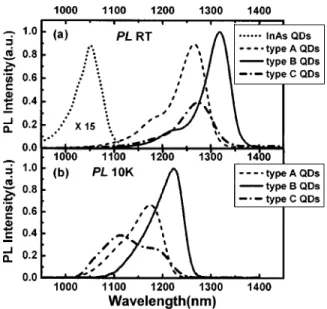
⫻1010to 1.7⫻1011cm⫺2. Figure 2共a兲 shows the room tem-perature PL spectra of these samples. The PL peak wave-length of InAs, type-A, type-B, and type-C QDs are 1051, 1267, 1318, and 1279 nm, respectively. The corresponding full width at half maximum共FWHM兲 linewidths are 66, 54, 44, and 60 meV. The structural parameters and measured photoluminescence of these four QD samples are summa-rized in Table I. The deposition method of the InGaAs cap-ping layer influences both the dot density and the emission wavelength of InAs/InGaAs QDs. This can be explained by the redistribution of In and Ga atoms during the deposition of the InGaAs capping layer on InAs QDs.11A strain field caused by InAs QDs induces the preferential migration of In atoms to InAs QDs and Ga atoms from the dots. Further-more, during the overgrowth of the high-In-content InGaAs, new islands are generated at the nucleation center of the InAs wetting layer. In and Ga atoms have longer surface migration lengths in type-B QDs as compared with those in type-C QDs. Thus more In atoms can migrate to InAs QDs, and hence type-B QDs have bigger dot size and lower dot den-sity. On the other hand, the MBE method provides shorter migration lengths for the adatoms and thus has higher
prob-ability of nucleating new islands. Though both the QD size and density increase after capping the high-content In-GaAs layer in type-B and type-C QDs, the former method gives bigger dot size and significant redshift on the emission wavelength. In type-A QDs, the desorption of In atoms may take place during the interruption stage because of lacking As2 protection. InAs QDs with smaller size could disappear due to the desorption of its In content, and result in even a lower dot density than InAs QDs without InGaAs capping layers. In the deposition of the covering InGaAs layer of type-A QDs, In and As were co-deposited. In fact, interrup-tion of As supply during the In deposiinterrup-tion was also tested, and the dot density is even lower. However, the strongest migration ability provided by migration enhanced epitaxy method may greatly enhance the size of the surviving QDs, which is the biggest among the three methods as can be seen in the figures. The vertical exchange of In and Ga atoms in migration enhanced epitaxy has been ever reported.12 Ac-cording to this theory, the In atoms of the InAs QD and its covering layer may be replaced by Ga atoms, and the reduc-tion of In content in both the dot and covering layer leads to a blueshift in PL transition due to the increment of the band gap energy. Although type-A QDs has the biggest dot size, the reduction in In content dominates the PL characteristics and results in a shorter peak wavelength as compared with type-B and type-C QDs. Figure 2共b兲 displays the 10 K PL spectra of type-A, type-B, and type-C QDs. The spectrum of type-C QDs shows two peaks, while type-A and type-B QDs show only one peak. This indicates that there are two groups of QDs coexisting in type-C QDs. This result supports our point that besides the InAs QDs under the InGaAs capping layer, new InGaAs QDs also nucleated on the InAs wetting layer or InGaAs layer in type-C QDs. Although the dot den-sity of type-B QDs is slightly higher than that of InAs QDs, the single peak in their 10 K PL spectra reveals that most of type-B QDs are InAs/InGaAs QDs. The results in Ref. 11 show that there is a drastic decrease in PL intensity at 1.3m wavelength region when the In composition of InGaAs cap-ping layer grown by MBE method is over 30%. However, in our study, we found that the wavelength of type-B QDs can be extended to 1.3m without optical degradation when In composition of 33% is used.
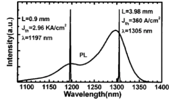
The room temperature lasing and PL spectra of the three-stack type-B QD lasers are shown in Fig. 3. The PL was measured after the GaAs contact layer and InGaP upper clad-ding layer were removed. Two PL maxima corresponclad-ding to the ground state and first excited state are clearly observed. For as-cleaved lasers with cavity lengths of 3.98 and 0.9 mm, the lasing wavelengths are 1305 and 1197 nm, and the
cor-FIG. 1. SEM images of共a兲 InAs QDs, 共b兲 type-A QDs, 共c兲 type-B QDs, and
共d兲 type-C QDs.
FIG. 2.共a兲 Room temperature PL spectra of InAs QDs, type-A, type-B, and type-C QDs.共b兲 PL spectra at 10 K of type-A, type-B, and type-C QDs. The SEM images of these samples are presented in Fig. 1.
TABLE I. Summary of structural parameters and measured photolumines-cence of InAs QDs, InAs covered by Ga/InAs supply共type-A QDs兲, InAs covered by GaAs/InAs sequential binary growth 共type-B QDs兲, and InAs and InGaAs with usual MBE growth共type-C QDs兲.
QDs Dot density (cm⫺2) Dot diameter 共nm兲 PL peak wavelength共nm兲 FWHM 共meV兲 InAs QDs 6.9⫻1010 20 1051 66 type-A QDs 2.3⫻1010 34 1267 54 type-B QDs 7.6⫻1010 29 1318 44 type-C QDs 1.7⫻1011 27 1279 60
4478 Appl. Phys. Lett., Vol. 82, No. 25, 23 June 2003 Chang, Wu, and Lin
responding threshold current densities are 360 A/cm2 and 2.96 kA/cm2. The threshold current density and the lasing wavelength versus reciprocal cavity length plot of type-B QD laser are shown in Fig. 4. The lasing wavelength de-creases from 1305 to 1193 nm, and the threshold current density increases from 360 A/cm2 to 4.84 kA/cm2, as the cavity length is decreased from 3.98 to 0.64 mm. When the cavity length is 0.96 mm, two lasing lines corresponding to the ground state and first excited state transition are observed at the current density of 1.35 Jth. This reveals the competi-tion between the ground-state and excited-state transicompeti-tions at the pumping level close to the gain saturation of the ground state. As the cavity length is shorter than 0.96 mm, the lasing line shifts from the ground state to the first excited state, and the threshold current density jumps to 2.96 kA/cm2 abruptly. This can be attributed to the gain saturation of the ground state. As the cavity length is decreased, the mirror loss in-creases and finally makes the total loss larger than the satu-ration gain of the ground state. As a result, the device is forced to lase at the first excited state, which has higher order of degeneracy and thus a higher saturation gain and transpar-ency current density. Using linear fit on the plot of inversed external quantum efficiency versus cavity length, the
de-duced internal loss (␣i) and internal quantum efficiency (i)
of the ground state in this laser are 4.82 cm⫺1 and 28.3%, respectively. Using the condition that the gain is equal to the total losses 共cavity and mirror兲 on the laser with 0.96-mm-long cavity, we can find that the saturation gain of the ground state is 16.6 cm⫺1.
In summary, we have studied the effects of high-In-content InGaAs capping layer on the structural and optical properties of the QDs. By using different capping methods, the quantum-dot density can be controllably changed from 2.3⫻1010to 1.7⫻1011 cm⫺2without a pronounced decrease in PL intensity. QDs with the capping layer grown by GaAs/ InAs sequential binary growth method 共type-B QDs兲 have a dot density as high as 7.6⫻1010cm⫺2 and a photolumines-cence peak at 1318 nm. We also investigated the character-istics of lasers with type-B QD medium. For an as-cleaved laser with a cavity length of 3.98 mm, the lasing wavelength is 1305 nm and threshold current density is 360 A/cm2. By changing the cavity length, the step-like jumps of the lasing wavelength and threshold current density due to the gain saturation of the ground state are observed. The ground-state saturation gain of the type-B QD laser is 16.6 cm⫺1.
This work was supported by the National Science Coun-cil of the Republic of China under Contract No. NSC 91-2120-E-002-004.
1
P. G. Eliseev, H. Li, A. Stintz, G. T. Liu, T. C. Newell, K. J. Malloy, and L. F. Lester, Appl. Phys. Lett. 77, 262共2000兲.
2G. Park, O. B. Shchekin, S. Csutak, D. L. Huffaker, Z. Zou, and D. G. Deppe, Appl. Phys. Lett. 75, 3267共1999兲.
3
M. V. Maximov, I. V. Kochnev, Y. M. Shernyakov, S. V. Zaitsev, N. Y. Gordeev, A. F. Tsatsul’nikov, A. V. Sakharov, I. L. Krestnikov, P. S. Kop’ev, Z. I. Alferov, N. N. Ledentsov, D. Bimberg, A. O. Kosogov, P. Werner, and U. Gosele, Jpn. J. Appl. Phys., Part 1 36, 4221共1997兲. 4G. Park, D. L. Huffaker, Z. Zou, and D. G. Deppe, IEEE Photonics
Tech-nol. Lett. 11, 301共1999兲.
5V. M. Ustinov, A. E. Zhukov, N. A. Maleev, A. R. Kovsh, S. S. Mikhrin, B. V. Volovik, Yu. G. Musikhin, Yu. M. Shernyakov, M. V. Maximov, A. F. Tsatsul’nikov, N. N. Ledentsov, Zh. I. Alferov, J. A. Lott, and D. Bimberg, J. Cryst. Growth 227–228, 1155共2001兲.
6
A. Stintz, G. T. Liu, H. Li, L. F. Lester, and J. M. Malloy, IEEE Photonics Technol. Lett. 12, 591共2000兲.
7K. Nishi, H. Saito, S. Sugou, and J. S. Lee, Appl. Phys. Lett. 74, 1111
共1999兲.
8
G. Park, O. B. Shchekin, D. L. Huffaker, and D. G. Deppe, IEEE Photo-nics Technol. Lett. 13, 230共2000兲.
9A. Stintz, G. T. Liu, A. L. Gray, R. Spillers, S. M. Delgado, and K. J. Malloy, J. Vac. Sci. Technol. B 18, 1496共2000兲.
10N. T. Yeh, T. E. Nee, J. I. Chyi, C. T. Chia, T. M. Hsu, and C. C. Huang, J. Cryst. Growth 227–228, 1044共2001兲.
11M. V. Maximov, A. F. Tsatsul’nikov, B. V. Volovik, D. S. Sizov, Yu. M. Shernyakov, I. N. Kaiander, A. E. Zhukov, A. R. Kovsh, S. S. Mikhrin, V. M. Ustinov, and Zh. I. Alferov, Phys. Rev. B 62, 16671共2000兲. 12
H. Yamaguchi and Y. Horikoshi, J. Appl. Phys. 68, 1610共1990兲.
.
FIG. 3. PL and lasing spectra for InAs/InGaAs QD lasers with type-B QDs.
FIG. 4. Threshold current density and lasing wavelength vs reciprocal cav-ity length plot for type-B QD lasers.
4479
Appl. Phys. Lett., Vol. 82, No. 25, 23 June 2003 Chang, Wu, and Lin