γ κ ˃ ደ
理學院應用科技學程
碩 士 論 文
全數位控制寬頻振盪器之研究
The study of Wideband, Cell-based Digital
Controlled Oscillator and its Implementations
研究生 : 賴榮欽
指導教授 : 許騰尹 教授
全數位控制寬頻振盪器之研究
The study of Wideband, Cell-based Digital
Controlled Oscillator and its Implementations
研 究 生:賴榮欽
Student : Jung-Chin Lai
指導教授:許騰尹
Advisor : Terng-Yin Hsu
國 立 交 通 大 學
理學院應用科技學程
碩 士 論 文
A Thesis
Submitted to Degree Program of Applied Science and Technology
College of Science
National Chiao Tung University
in partial Fulfillment of the Requirements
for the Degree of
Master
in
Degree Program of Applied Science and Technology
June 2007
Hsinchu, Taiwan, Republic of China
中華民國九十六年六月
全數位控制寬頻振盪器之研究
學生:賴榮欽 指導教授:許騰尹國立交通大學理學院應用科技專班
摘要
這個論文研究全數位鎖相回路振盪器之研究.。如何增加頻寬,,增高解析度 和降低抖動的影嚮是我們全篇論文的重點。我們的設計是一個寬頻的輸出,我們 可以輸出的頻率從 0.66~460 MHz,每一步可以改變 2.16 奈秒。這個設計是一個 數位訊號轉換為時間的設計,我們用數位訊號改變輸出的頻寬。我們在這裡也用 到 AOI 和 OAI 作為微調的元件,這個元件可以提供 0.01 皮秒(pico-seconds)的 解析度。為了降低抖動,我們使用電流鏡來達成我們的目的。如同眾所周知的, 電感、電阻和電容的效應將使瞬間的電流破壞電壓源的穩定度,也將使得輸出的 訊號不停的抖動。電流鏡可以使我們的設計穩定電壓源,也使得輸出的訊號更 好。我們這篇論文的重點就會在寬頻、高解析度及降低抖動上面。從一些模擬的 實驗上就可以看出我們設計的效果。我們更將把這個設計做到晶片上面,從實際 的晶片來驗證我們設計的效果。The study of Wideband, Cell-based Digital Controlled
Oscillator and its Implementations
Student: Jung-Chin, Lai Advisor: Dr. Terng-Yin Hsu
Degree Program of Applied Science and Technology
National Chiao Tung University
ABSTRACT
The thesis is based on All-digital-Phase-Locked- Loops (ADPLL).. We will discuss wide band, cell-based digital controlled oscillator (DCO) in this thesis. In our design, there is a wide bandwidth DCO. The frequency is from 0.66~ 460MHz step by 2.16ns. It is designed by Digital-to-Time (DTC) scheme. We also use AOI and OAI as Fine-tune cells. The best resolution of this design is 0.01 pico-seconds. We use UMC 90nm standard cell AOI to get this performance. In another way, we put current mirror in DCO for reduction of bounce noise. That will effectively reduce jitter caused by ground bounce. The wide bandwidth DCO use DTC to do the internal count for different bandwidth. That is a double loops scheme. AOI cell is the standard cell for fine tune solution. When we change the control bits of AOI, it change the capacitance of additional capacitor. The resolution of 0.01 pico-seconds is a good performance for DCO design. The output jitter is another issue. When the design is working, the transient current will make a serious ground bounce. It is the major source of jitter. How to reduce the ground bounce and jitter is the important topic for DCO design. Here we use current mirror to reduce the ground bounce and make the clean signal.
誌 謝
在碩士專班這幾年的學習中,感謝家人的體諒與配合,讓我可以在學業及工 作全力衝刺,而無後顧之憂。除了家人之外,最感謝的人是我的指導教授許騰尹 博士,許老師因才施教,對學生無私的指導與愛護,令人感佩。感謝老師的事太 多,非一二言所能盡,只能說跟許老師研究是學子之福。也感謝實驗室學長及同 學的幫忙,有一個好的研究環境與平臺,使得實驗可以順利進行。感謝專班主任 莊祚敏博士為學生創造學習機會,讓我有機會在回到學校學習。個人力量太小, 受人之惠太多,謝謝曾幫過我的所有人。Contents
Chapter 1 Introduction ...1
1.1 Thesis Background... 1 1.2 Thesis Motivation ... 2 1.3 Thesis Contribution... 2 1.4 Thesis Organization ... 3Chapter 2 Basic concept of DCO Implementations (DCO) ...4
2.1 All-Digital-Phase-Locked-Loop (ADPLL)... 4
2.2 The basic concept of Digital-Controlled Oscillator (DCO) ... 5
2.2.1 Coarse-tune unit ... 6
2.2.2 Fine-tune unit ... 7
Chapter 3 Proposed Digital-Controlled-Oscillator (DCO) and
simulation result ...9
3.1 Overview of the proposed Digital-Controlled Oscillator... 9
3.2 The proposed DCO architecture ... 13
3.3 Cell-based Digital Controlled Oscillator ... 15
3.3.1 Digital to time converter (DCO) ... 15
3.3.2 Coarse-tune cell ... 18
3.3.3 Fine-tune cell ... 19
3.3.4 Performance comparison with other work ... 24
3.4 Current mirror for jitter reduction... 24
Chapter 4 Discussion and Future Work...27
4.1 Discussion ... 27
List of Figures
Fig. 2.1 ADPLL block diagram... 4
Fig 2.2 basic concept of DCO architecture ... 5
Fig 2.3 Inverter chain as coarse-tune cell... 6
Fig 2.4 Inverter and nand chain as coarse-tune cell ... 6
Fig 2.5 Current-starved ring oscillator as fine-tune cell... 7
Fig 2.6 Fine-tune unit with additional capacitor ... 7
Fig 2.7 inverter gate as additional capacitor ... 8
Fig 2.8 Nor gate as additional capacitor... 8
Fig 2.9 Fine-tune unit with phase mixer ... 8
Fig 3.1 DCO digital controller ... 9
Fig 3.2(a) DCO block ... 10
Fig 3.2(b) clock period in different frequency... 10
Fig 3.3(a) clock period in different frequency... 11
Fig 3.3(b) inverter intrinsic delay ... 12
Fig 3.3(c) clock period in different frequency with additional NMOS capacitor ... 12
Fig3.4 NMOS gate capacitor in three regin UMC 90um NMOS W/L=0.33um /0.08um ... 13
Fig 3.5 DCO controlled by digital signal ... 14
Fig 3.6 proposed DCO architecture... 15
Fig3.7 Digital-to-time converter DTC for wide bandwidth ---C1[8:0] band width tuning up ... 16
Fig 3.8(a) DTC clock period increase by 3.026ns ... 16
Fig 3.8(b) minimum clock period 2.16ns and maximum clock period 1548.5ns. ... 17
Fig3.8(c) minimum clock period 2.16ns is consist of DTC, Coarse-tune cell and Fine-tune cell intrinsic delay time. Clock period is 2.16ns + 2*C1[8:0] (internal clock period)... 17
Fig 3.8(d) Coarse–tune cell... 18
Fig 3.9 ine-tune cell as capacitance adjustment by control the switches F1 F2 F3 and F4 Fine-tune cell as capacitors and capacitance is adjusted by switches... 20 Fig 3.10(a) F1 Fine-tune cell simulation result. Each step of Fine-tune delay time is
4ps ... 21 Fig.3.10(b) F2 Fine-tune cell simulation result. Each step of Fine-tune delay time is
0.15ps. Here we get waveform every 4 steps, that is 0.6ps ... 21 Fig 3.11 OAI as Fine-tune cell ... 22 Fig 3.12 F3 Fine-tune cell simulation result. Each step of Fine-tune delay time is
0.05ps ... 22 Fig 3.13 AOI as Fine-tune cell ... 23 Fig 3.14 F4 Fine-tune cell simulation result. Each step of Fine-tune delay time is
0.01ps ... 23 Fig 3.15 DCO with current mirror ... 25 Fig 3.16 The simulation result of DCO. The ground bounce is from 0.44V
reduced to 0.187V and internal_clock of DTC is improved after the current mirror is applied... 25 Fig 3.17 The period of DTC internal_clock. For the experiment without current
mirror, RMS=0.1448ns and peak-to-peak is 0.418ns. For the experiment using current mirror, RMS=0.0094ns and peak_to_peak is 0.03ps. ... 26
List of Tables
table 3.1 ... 14
table 3.2 ... 19
table 3.3 The resolution of AOI/OAI as Fine-tune-cell for different switching ... 24
CHAPTER 1
INTRODUCTION
1.1 Thesis
Background
In modern SoC design, the clock quality is very important, including frequency, phase, duty cycle and jitter. Phase Locked Loops (PLL) and Delay-Locked Loops (DLL) are good solutions for clock quality and widely utilized for clock circuit. Precise duty cycle and low jitter are required for high-speed and low-power circuit design. We can integrate PLL or DLL circuit into systems for many applications -LCD driver, tuner of the digital TV, synchronous DRAM, wireless system, video player, etc.
Phase Locked Loops ( PLL) and Delay-Locked Loops (DLL) circuits are often used as clock generator, frequency synthesizers, clock de-skewing and clock data recovery for microprocessors. PLL is used to multiply the clock frequency and then align the edges of the distributed output clock to the received clock. It is basically a closed loop frequency control system, which is based on the phase sensitive detection of phase difference between the input and output signals of the controlled oscillator. The PLL accomplishes this task by adjusting the frequency of a voltage-controlled oscillator (VCO) or digital-controlled oscillator (DCO) which drives the output clock so that the distributed clock, once divided in half and fed back to the PLL, matches frequency and lines up with the received clock. This simple application requires certain features in the PLL, like the ability to accept a feedback clock and the ability to multiply the input frequency.
The good design of PLL-based clock generator considers high frequency/phase resolution, fast lock-in time, low jitter performance, low power consumptionh, low area cost. It is a trade-off and it is not easy to meet all consideration we need. Design time is also a significant issue. How to quickly finish the design task and tape out is very important. For the purpose to meet many applications, wide bandwidth is another request. But bandwidth need more area cost and power consumption.
In System-on-a-Chip (SoC) design, the cell can be reusable and process is a good way to reduce design time. Design time is very important for time-to-market. Most PLL design use mixed signal and integrated with digital design. That will spend long time to do full customized design. How to develop a All-digital-Phase-Locked-Loops (ADPLL) become a more and more important task. ADPLL can be easily implemented in different process generation with few ultra tasks.
1.2 Thesis
Motivation
The thesis is based on All-digital-Phase-Locked-Loops (ADPLL). There are several advantages for ADPLL design over their analog counterparts [1]. The advantages include lower power consumption [2], easy to change with scaling in different process and no DC offset issue as analog design [3].
There are an ever-increasing number of portable applications requiring low power design concept. For example, notebook, cellular phone, PDA , digital camera, full-motion video and audio. etc. There are three major sources of power dissipation in CMOS circuit in the equation below,
Ptotal = pt(CL .V.Vdd.fclk) + Isc.Vdd + Ileakage.Vdd (1.1)
The first term is the switching component of power, pt is the probability that a power-consuming transition occurs. The second term is direct-path short current. The third term is leakage current arise from substrate injection and subthreshold effects. In the “well-designed” circuit, the dominant term is switching component. We can minimize pt, CL, Vdd to meet our low power target.
For time-to-market propose, it can reduce both design time and design complexity by using Verilog hardware-description language. And it is easy to implemented by auto placing and routing (APR) tools. For different process migration, it is not necessary to change behavior of digital with scaling, the only effort is to synthesize with new library and put it to layout by APR. If we use analog design, we need to re-design the circuit and implement to layout by manual. It will spend much time to do a good analog circuit.
The supply voltage is usually decreased when the technology is migrated to more advanced CMOS processes. So that the voltage headroom and signal swing of transistor is also decreased. This will suffer the performance of analog design.
All digital cell-based approach is preferred to SoC design due to these reasons. To develop a high resolution, wide bandwidth and low jitter ADPLL is the motivation of this thesis.
1.3 Thesis
Contribution
In this thesis, we will introduce the scheme to gain high resolution and wide bandwidth for ADPLL design. We also use some analog scheme to reduce jitter and gain better performance.
● Use Digital-to-Time converter (DTC) to gain wide bandwidth
DTC is the design for wide bandwidth DCO. Our design provide the wide bandwidth from 0.66~460MHz. The wide-bandwidth can be used in more modules.
● AOI/OAI as fine tune cell to gain the high resolution.
We use AOI/OAI gate as additional capacitor. The resolution of AOI-based cell is 0.01ps. And that is 0.05ps for OAI-based cell. AOI and OAI are both standard cell and easy to implement in design.
● Add current mirror to DCO ground source for reducing ground bouncing
noise and reducing jitter
For high resolution ADPLL, the clear power source is necessary for Digital- Controlled-Oscillator (DCO). Current mirror is an effective method to reduce power/ground noise. But the current mirror is an analog design and it is not easy to integrate into digital design.
1.4 Thesis
Organization
In chapter1, we introduce the application of Phase-Locked-Loop (PLL), the significance of PLL .We also introduce the advantage of All-Digital-Phase-Locked-Loop (ADPLL) and why we prefer digital-based cell than analog-based cell. Finally, we introduce the contribution and the organization in this thesis.
In chapter2, we will give an overview of Digital-Controlled-Oscillator (DCO). DCO is the core of ADPLL. It is consist of Coarse-tune cell and Fine-tune Cell. Here we will introduce the overview of Coarse-tune cell and Fine-tune cell.
In chapter3, we will introduce the proposed DCO. We use Digital-to-Time converter (DTC) for wide bandwidth control. The bandwidth we provide in our design is from 0.66~460MHz. It is really wide bandwidth scheme. We have one Coarse-tune cell and four Fine-tune cells for frequency adjustment. Coarse-tune cell is consist of inverter and NAND delay chain and controlled by multiplex. We have for Fine-tune cells. The first cell is consist of two parallel NAND gate. The second cell is only one NAND gate. The third cell is OAI standard cell. The fourth cell is AOI standard cell. We use Fine-tune cell as additional capacitor in the delay line. We adjust the additional capacitance by control bits.
In chapter4, conclusion will be derived here from this research. Finally, we describe some design issue for future work here.
CHAPTER 2
BASIC CONCEPT OF DCO
IMPLEMENTATIONS
In this chapter, we will introduce the basic concept of Digital-Controlled oscillator. First, we introduce the basic concept of ADPLL. Then, we will introduce DCO. That is the major topic we discuss in this thesis
2.1 All-Digital-Phase-Locked-Loop
(ADPLL)
All-Digital-Phase-Locked-Loop (ADPLL) is designed with digital design technology. It is scalable with different process generations. The diagram block is show as Fig.2.2 [4][5][6]. The frequency/phase detector detect the frequency/phase difference between reference clock(REF_CK) and divided output clock(CK_divM). The frequency-gain register and phase-gain register provide operands to the adder and subtracter. And the phase-gain register also provides data to the anchor circuit. The anchor register stores the baseline frequency. Finally, DCO controller provides the control bits to DCO and generates expected output clock (DCO_ CK). In addition, frequency divider here is to divide the output frequency into the reference frequency.
2.2 The Basic Concept of Digital-Controlled
Oscillator (DCO)
Digital-Controlled Oscillator is the heart of ADPLL, the resolution of fine-search is the key factor of jitter performance. We will introduce the high resolution DCO in the next chapter. Here we just introduce the basic concept of DCO.
The Basic concept of DCO is show as Fig.2.2.[7][8][9]. The DCO include Coarse-tune unit(CTU) and Fine-tune unit(FTU). The total loop delay (τ_DCO) is
show as eq. (2.1),whereτ_FTU is the total gate delay of fine-tune stage,τ_CTU is the
total gate delay of CTU and τ _intrinsic is the intrinsic delay of data path and
multiplexer . When N Coarse-tune stages are switched on, the τ_CTU is described as
(2.2), whereτ_C is the timing delay of one coarse-tune stage. The maximum period
of DCO is 2‧τ_DCO and the minimum period of DCO is 2‧(τ_FTU+τ_intrinsic)
when all of Coarse-tune cells are turn off. The frequency range of operation is fmin to
fmax. fmin is the reciprocal of minimum period described as eq. (2.3) and fmax is the
reciprocal of maximum period described as eq.(2.4). We can get the frequency between fmin and fmax due to different controlled bits. The set of controlled bits is
decided by ADPLL controller.
τ_DCO = 2‧(τ_CTU +τ_FTU +τ_intrinsic) (2.1)
τ_CTU =N‧τ_C (2.2)
fmax = 1/ [2‧(τ_FTU+τ_intrinsic) ] (2.3)
2.2.1 Coarse-tune unit
The most used Coarse-tune unit is based on inverter delay chain [10][11][12][13] [14] [17]as Fig.2.3. The unit coarse delay timeτ_C is consist of one inverter rise time
and one inverter fall time as eq.(2.5). The rise time is the charge time through PMOS as eq.(2.6). RP is the resistance of PMOS channel and Cg is the capacitance of inverter gate. The fall time is the discharge time through NMOS as eq.(2.7). RN is the resistance of NMOS channel. We can adjust the W/L of inverter to decide the unit coarse delay timeτ_C.
τ_C = τ_rise +τ_fall (2.5)
τ_rise = RP ‧ Cg (2.6)
τ_fall = RN ‧ Cg (2.7)
Furthermore, we use nand as Coarse-tune cell for power saving design as Fig.2.4. In this scheme, the non-used delay chain is turn off to avoid transient power consumption.
2.2.2 Fine-tune unit
The resolution of Fine-tune unit is regarded to the performance of DCO clock. How to improve the fine tune resolution is the important way to reduce the jitter. It is difficult to reduce the jitter if the fine tune resolution is not as good as low jitter requirement.
The well-known Fine-tune unit is described as Fig.2.5.[6][15][16][17]. The Fine-tune unit has two transistors turn-on to be the loading of inverter. There are several transistor pairs controlled by fine tune control bits. Through the control of these bits, we adjust the loading of inverter and get the different delay time.
For example, we have 4 bits to control the fine tune delay. Assume the loading of control bits set (f1:f4)=(0000) is RL. The loading of control bits set (f1:f4)= (1111) will
be 5 RL. We have 5 steps delay time when (f1:f4)=(0000)/(0001)/(0011)
/(0111)/(1111).
The other method of Fine-tune unit is to add the additional capacitor in the delay chain as Fig.2.6.[1].
Each capacitor provide the additional capacitance △C .We can change the amount of connected capacitors and adjust the delay time through the control bits. We can have inverter gate or one pair of transistors (PMOS & NMOS) to be the additional capacitor as Fig.2.7. Nor gate and Nand gate are also the good solutions for better fine tune resolution. We will introduce OAI and AOI as additional capacitor in next chapter. The △C of them is much smaller than others so we can have the best resolution as delay time step.
The third method of fine-tune unit is phase-mixer as Fig.2.9.[18][19]. Through mixing early and late signals as different phase, we can get the different fine tune steps. The design constraint of the phase-blender circuit is that all paths through the circuit must provide precisely the same loading and delay time to make sure the phase difference of ψA andψB is the same as ΨA andΨB. The phase-mixer can have
CHAPTER 3
PROPOSED
DIGITAL-CONTROLLED-OSCILLAT
OR (DCO) AND SIMULATION
RESULT
In analog PLL, Voltage-Controlled-Oscillator (VCO) is used to generate the phase-locked clock. As the same function of VCO, DCO is implemented to All-Digital-Phase-Locked-Loop (ADPLL) for clock generation as Fig.3.1. DCO accept the digital signals from controller and transfer the digital signals to time delay. The delay time will decide the phase and frequency of oscillator. That is, ADPLL controls the DCO by changes the control words. Arithmetically incrementing or decrementing the DCO control words will modulate the DCO frequency and phase.
Here we also provide the wide bandwidth DCO. Digital- to-Time Converter (DTC) is applied to decide wide bandwidth frequency. Through digital signals control, wide bandwidth application is available. In this chapter, we introduce the overview structure of Digital-Controlled Oscillator (DCO), coarse- search cell, fine-search cell and the new scheme to get better fine search resolution. In next section, we will introduce Digital-to-Time Converter (DTC) and wide bandwidth oscillator scheme. In addition, how to reduce jitter from DCO scheme is the other important topic that we will discuss.
The DCO block of ADPLL consists of Digital-to-Time converter (DTC), Coarse-search cell and Fine-search cell as Fig.3.2 (a).
DTC is designed for wide bandwidth application. Coarse-search cell is designed for coarse search that search step is large. Fine-search cell is designed for fine search that search step is small. When the clock signal rise, the delay path through DTC, Coarse-search cell and cell make the delay time as period of duty cycle “high”(TH). In the other hand, the clock signal falls, the delay path makes the delay time as period of duty cycle “low”(TL). The consistent of duty cycle “high” and duty cycle “low” make the whole clock cycle. The period of clock(T) is sum of the period of duty cycle “high” and duty cycle “low”. As show in Fig.3.2(b), T = TL + TH.. The frequency f is 1 divide T, that is, 1/T. For example, if TL=0.5 ns and TH=0.5ns, T = TL + TH = 1ns, the frequency is 1/1ns = 1GHz.
The basic concept of oscillator is show as Fig.3.3(a). There is intrinsic delay exists in m1, m2 and m3. The intrinsic delay caused by resistance in MOS channel and capacitance in loading capacitor. Fig.3.3(b) shows intrinsic delay of inverter.
When signal rise, current come from VDD and charge loading capacitor. The time delay τ_rise =” Rp ‧ Cg”. On the other way, current discharge from loading capacitor to ground when signal falls, the time delay τ_fall =” Rn ‧ Cg”.
τ_rise = Rp ‧ Cg (3.1)
τ_fall = Rn ‧ Cg (3.2)
The oscillator consists of 3 ( or odd) inverters . We replace one inverter with nand cell for the implementation of “Clock_EN”. The signal enable oscillator to work. At the moment when “Clock_OUT” signal rises, the time is t_r. After intrinsic delay time d1 of m1, “N1” signal falls to the inverse phase. After more m2 intrinsic delay time d2 , “N2” signal will rises to “H”. More time delay d3 is contributed from m3 . Finally, “Clock_OUT” falls at the time t_f = “t_r + d1 + d2 +d3”. “Clock_OUT” spend the time “d1 + d2 + d3” to travel on signal “H”. This is the period of clock duty “H”. It will travel on signal “L” at the same way and that will be the period of clock duty “L”. The balance of duty “H” and duty “L” is very important. It will significally influence the performance of DCO.
In this oscillator scheme, the period of duty “H” is contributed from two parts. One is fall delay of m1 and m3. The other one is rise delay of m2. On the other hand, the period of duty “L” is also contributed from two parts. One is rise delay of m1 and m3. The other one is fall delay of m2. How to get the same delay time at rising edge and falling edge is the serious topic in oscillator design.
We can add the additional gate capacitor in the delay chain. For example, we add a NMOS capacitor at net :”N1” as show in Fig 3.3(c). It spends more rise and fall time to charge the additional capacitor. The delay time d1 will be more than the original scheme. We can make several schematic by add different additional capacitor to get the different delay time. This will make the different frequency clocks. If the additional capacitance is large, it is the Coarse-search cell. If the additional capacitance is small, it is the Fine-search cell. Coarse-search cell is easy to implement, but the Fine-search cell is dependent on how much small the capacitance is. The most small step delay time is the best resolution in this design.
NMOS capacitance for different gate voltage is show in Fig.3.4. There are three regions in this plot.
(1) Accumulation occurs when Vg < Vfb, the negative charge on the gate attracts holes from the substrate to the oxide-semiconductor interface.
(2) Depletion occurs when Vfb < Vg < Vth, the positive charge on the gate pushes the mobile holes into the substrate. Therefore, the semiconductor is depleted of mobile carriers at the interface and a negative charge, due to the ionized acceptor ions, is left in the space charge region.
(3) Inversion occurs when Vg > Vth, there exists a negatively charged inversion layer at he oxide-semiconductor interface. The inversion layer is caused by minority carriers, which are attracted to the interface by the positive gate voltage.
From the plot we find that the capacitance is different at VN1=0v and VN1=1v. At VN1=0v, the NMOS capacitance is in depletion region. But at VN1=1v, the NMOS capacitance is in inversion region. That is, the rise delay is different from the fall delay. In the circuit design, we usually add another PMOS to get the better performance for time delay. In the DCO design proposed here, the delay cell for search steps are Inverter, NAND and OAI. The gate capacitors of these cells both have NMOS and PMOS. NOR and AOI are also the good delay cells for search steps.
3.2 The proposed DCO architecture
reduce jitter is another important topic. We will discuss the scheme integrated with analog design for reducing later.
As the diagram show in Fig.3.5, DCO receives the control bits from DCO controller and generate the output clock. The frequency of this clock will be divided and compare with the reference clock. The result of comparison will make a new setting of control bits and generate a new DCO clock until both the phase and frequency is locked in.
The proposed DCO architecture is show as Fig.3.6. There are three major blocks in this scheme. The first block is Digital-to-Time converter for wide bandwidth control. The second block is Coarse-tune cell consists of inverter and NAND. The six control bits are decoded to 64 stages. The stage starts at C0 [5:0] = [000000] (en[30:0] = [00000…000]) and ends at C0 [5:0] = [111111] ( en[30:0] = [11111…111]). The delay time of each stage is 30 pico-seconds. The third block is Fine-tune cell. This cell includes four sub-cell and controlled by 13 bits. The first sub-cell is controlled by 3 bits and decoded to 8 stages. The stage starts at F1 [6:0] = [0000000] and ends at F1 [6:0]=[11111111]. The delay time of each stage is 4 pico-seconds. The second sub-cell is controlled by 5 bits and decode to 32 stages. The stage starts at F2 [ 30:0] = [00000…000] and ends at F2 [30:0] = [11111…111]. The delay time of each stage is 0.15 pico-seconds. The third sub-cell is controlled by 2 bits and decoded to 4 stages. The stages are F3 [2:0] = [000], [001],[011] and [111]. The delay time of each stage is 0.05 pico-seconds. The last sub-cell is controlled by 3 bits and decoded to 8 stages. The stage starts at F4[6:0]=[0000000] and ends at F4[6:0]=[1111111].
table.3.1 Coarse-search Fine-search First sub-cell Second sub-cell Third sub-cell Fourth sub-cell Cell name Inverter and
NAND NAND NAND OAI AOI
Control bits 6 3 5 2 3
stages 64 8 32 4 8
3.3 Cell-based Digital Controlled Oscillator
3.3.1 Digital to time converter (DTC)
DTC consist of internal CLK generator, counter and multiplex show as Fig.3.7. CLK generator is used to generate internal clock for timing counter. The “in” signal is come from “DCOCLK” as show in Fig.3.6. This signal is opposite to signal “out_reg” when it travels through all DCO delay cells. In this time, signal “EN” will go “H” and enable CLK generator. Counter begin to work . When the counter ends its work at the time that counter_reg [8:0] = C1 [8:0], signal “out_reg” will inverse to be the same as “in” through multiplex and continue to its next trip. The description above is the process about half cycle of clock. C1[8:0] decide the count number and clock period. When C1[8:0] add one, the clock period will add multiple of internal clock period 1.513ns. The minimum clock period is 2.16ns when C1[8:0]=0. The maximum clock period is 15148.5ns when C1[8:0]=511. That is, the frequency range is from 0.66MHz to 460MHz step by 3.026ns. The simulation result of variable clock period controlled by C1[8:0] is show as Fig.3.8(a) and that of minimum/maximum clock period is show in Fig.3.8(b).
The minimum clock period 2.16ns is consist of DTC, Coarse-tune and Fine-tune cell intrinsic delay when C1[8:0]=0. As C1[8:0] increase, the DCO clock period will
resolution. Wide bandwidth and high resolution is our design target. The advantage of DTC wide bandwidth is to overcome the variation of PVT.
3.3.2 Coarse-tune cell
The Coarse-tune cell is show as Fig.3.7. The delay chain consists of inverter and NAND. The delay time is selected by multiplex and controlled by C0[5:0]. There is a power saving scheme here. That is, we disable unused delay chain by en [30:0]. This scheme saves transient current. It will save current consumption and reduce the noise due to transient current. So it is a power saving and low jitter design.
From Fig.3.7 we can see that when mux[5:0]=[000000], the selected one is wire_l1_[0], the delay time is intrinsic delay due to 6 multiplexers and one inverter. When mux[5:0]=[000001], the selected one is inv_[1], the total delay time is one inverter and one Nand gate delay plus intrinsic delay. When mux[5:0]=[000010], the selected one is wire_l1_[2], the delay time is two Nand gate delay. The time delay from wire_l1_[0] to inv_[1] is 30ps and that from inv_[1] to wire_l1_[2] is also 30ps. That is, each stage delay time is 30ps. We have total 64 stages controlled by 6 bits. The first stage is intrinsic delay 450ps. The second stage delay is 480ps and the last stage delay is 450ps plus 1.89ns. The simulation result of coarse tune is as Fig.3.8. The minimum delay time of coarse is 450ps when mux[5:0]=[000000] and the maximum delay time is 450ps plus 1.89ns when mux[5:0]=[111111].
3.3.3 Fine-tune cell
We use four fine-tune cells, the advantage of this scheme is that it need fewer cell units. Because the coarse-tune cell resolution is 30ps, we need 3000 Fine-tune cell units that the resolution is 0.01ps for good work. In our scheme, we just need 48 Fine-tune cell units to meet our target as show in table3.2. This scheme will save more chip area. We need 12 control bits from DCO controller if we use 3000 F4 cell units. We need 13 control bits for our scheme because we have more tolerance in each stage for process, voltage and temperature variation. This penalty is a good deal for saving more Fine-tune unit cells.
table.3.2
Fine-search
First sub-cell Second sub-cell Third sub-cell Fourth sub-cell cell units number 7 31 3 7
start control set F1[0000000] F2[000…000] F3[000] F4[0000000] second control set F1[0000001] F2[000…001] F3[001] F4[0000001]
We have 2-NAND (F1), NAND (F2), OAI (F3) and AOI (F4) as Fine-tune cell. We decide the capacitance by controlling the switches. The switches are controlled by control bits of F1 [6:0], F2 [30:0], F3 [2:0] and F4 [6:0]. As described above, the change of capacitance means the change of delay time. By switching control bits, we can adjust the delay time to meet the target of frequency and phase. This is fine tune to meet DCO clock. As show in Fig.3.9., we can see F1, F2, F3 and F4 Fine-tune cell as addition capacitors. By controlling the switches, we adjust the capacitance to decide the delay time. NAND gate as F1 and F2 Fine-tune cell by adjustment of ΔC and ΔR. OAI as F3 Fine-tune cell and AOI as F4 Fine-tune cell by adjustment ofΔC, ΔR and ΔI.
F1 Fine-tune cell is consist of two parallel NAND gate, the channel width and length (W/L) of first NAND gate is equivalent to PMOS : W/L = 3.36u/0.08u and NMOS : W/L = 2.4u/0.08u. The channel width and length (W/L) of second NAND gate is equivalent to PMOS : W/L = 1.26u/0.08u and NMOS : W/L = 0.9u/0.08u.As Fig 3.10(a), each step of Fine-tune delay is 4 pico-seconds. From F1[6:0]=[0000000] to F1[6:0]=[0000001], the delay time will add 4 pico-seconds. From F1[6:0]=[00000 00] to F1[6:0]=[11111111], the delay time will add 28 pico-seconds. For the next increasing step, Coarse-tune will add one step of delay time that is 30 pico-seconds and F[6:0] reset to F1[0000000]. Here we have some tolerance for process, voltage and temperature variation. Our design for F1 Fine-tune cell can support Coarse-tune delay time by step 32 pico-seconds. We consider PVT issuse to have tolerance about 80%~90% for Coarse-tune cell and Fine-tune cell.
F2 Fine-tune cell is a NAND gate which channel width and length is PMOS : W/L = 0.36u/0.08u and NMOS : W/L = 0.24u/0.08u. The simulation result is show as Fig.3.10(b). Each step of F2 Fine-tune cell is 0.15 pico-seconds. Here we get waveform every 4 steps, that is 0.6 pico-seconds. From F2[30:0]=[000…000] to F2[30:0]=[111…111], total 32 stages. The delay time add 4.65 pico-seconds. This is more than F1 Fine-tune cell time delay 4 pico-seconds by step. This is also the consideration of PVT tolerance.
The simulation result of F3 Fine-tune cell is show in Fig.3.12(a). Each step of F3 Fine-tune cell is 0.05 pico-seconds. There are total 4 stages from F3[2:0]=[000] to F3[2:0]=[111]. The time delay from F3[000] to F3[001] is 0.015 pico-seconds and the time delay from F3[000] to F3[111] is 0.015 pico-seconds. For the next increasing step, F2 Fine-tune cell will add 0.15ps by one step. Here we also consider PVT variation and have more tolerance.
We use AOI as F4 Fine-tune cell that show in Fig.3.13. There are 4 pairs of PMOS/NMOS in this cell. Net “A1” is connected to delay line, net “B” is forced to “L” and net “C” is forced to “H”. When we switch the signal of net “A2” from ‘L” to ‘H”, the delay time will add 0.01ps. This is the best resolution we find in the cell of AOI and OAI.
The simulation result of F4 Fine-tune cell is show as Fig.3.14. Each step of delay cell is 0.01 pico-seconds. From the simulation waveform and measurement result, we can see the delay time is steadily increase 0.01 pico-seconds by step. This is reliable performance of Fine-tune cell. This also mean the jitter of this design can be reduced to be under 0.01 pico-seconds. From F4[6:0]=[0000000] to [0000001], the delay time add 0.01 pico-seconds. From F4[6:0]=[0000000] to [1111111], the delay time add 0.07 ps, this is more than F3 Fine-tune cell resolution 0.05ps. Here is also the consideration of PVT tolerance.
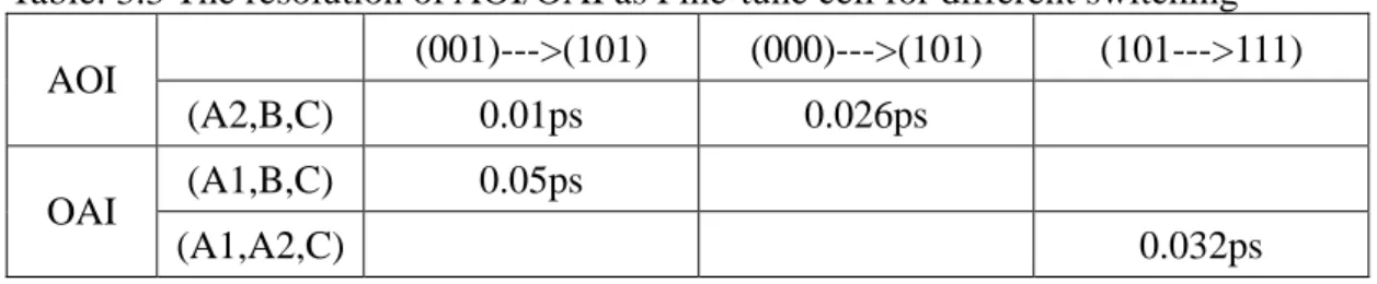
It is a interesting work to use AOI and OAI as Fine-tune cell. From the simulation result, we can find the reliable performance as table.3.3 It is reliable to use
Table. 3.3 The resolution of AOI/OAI as Fine-tune cell for different switching (001)--->(101) (000)--->(101) (101--->111) AOI (A2,B,C) 0.01ps 0.026ps (A1,B,C) 0.05ps OAI (A1,A2,C) 0.032ps
3.3.4 Performance comparison with other work
From the performance comparison as table.3.4 [1][8][20][5], we can find the performance of our design in bandwidth and LSB resolution is much better than other work. In the comparison of these work, we find the best bandwidth except our work is 45~450MHz. It is not so good as our design 0.66~460MHz (i.e.2.16ns ~ 15148.5 ns).
The best resolution of other design is 5 pico-seconds for Fine-tune cell. Our design is 0.01 pico-seconds. That is much better than others work. The Fine-tune resolution is related to jitter performance. The much better resolution will make good jitter performance. The other advantage of our design is low power, the power consumption is 1.15mW at 460MHz.
3.4 Current mirror for jitter reduction
There is a model to simulate the jitter induced by ground bounce due to transient current. We assume there is a 400MHz transient current induced by other 2000 inverters of ADPLL and make the bounce noise 0.44V. In our experiment, we have a current mirror sinking 10 mA in our DCO scheme and reduce bounce noise to 0.187V.
The experiment is show as Fig.3.15. We consider the RLC effect from package. The transient current will make power and ground bounce. That is the major source of jitter.
table 3.4 Performance comparison with other work
This work TCSII '05 ISQED '02 ISSCC'03 JSSC'03 0.09um @ 1V 0.35um @ 3.3V 0.5um @ 1.65V 0.6um @ 5V 0.35um @ 3.3V
DCO word length 28 bits 15bits 8 bits 10bits 12bits
LSB resolution 0.01 ps 1.55 ps 40 ps 10 ps 5 ps
DCO output range 0.66~460MHz 18~214MHz 150MHz 10~12.5MHz 45~450MHz Power Consumption1.15mW @ 460 MHz 18mW @ 200 MHz 1mW @ 150 MHz 164mW @ 100 MHz 100mW @ 450 MHz
We can find the simulation result in Fig.3.16. The power and ground bounce influence the period of clock. That will be the major source of jitter. If we apply current mirror for DCO., the bounce will be reduced. We find the internal clock of DTC will be improved when current mirror is applied. The internal clock of DTC is the clock of timer counter. The jitter will influence the DCO output clock.
The jitter of internal clock is show as Fig.3.17. The RMS of internal clock is 0.1448ns and peak-to peak is 0.418ns if current mirror is not applied. Our target period is 1.513ns. The peak-to peak shows the jitter is serious in this experiment. If we apply current mirror, the RMS will be 0.0094ns and peak-to-peak will reduce to 0.035ns. This experiment shows the performance of current mirror. By adjusting the bias current, we can get the best performance of jitter.
CHAPTER 4
DISCUSSION AND FUTURE WORK
4.1 Discussion
We have introduced basic DCO concept and the proposed DCO scheme in this thesis. DCO is the core of ADPLL. The performance of DCO is concerned by ADPLL design. We have to design a wide bandwidth, high resolution and low jitter DCO for high efficiency ADPLL.
In our design, there is a wide bandwidth DCO. The frequency is from 0.66~ 460MHz step by 2.16ns. It is designed by Digital-to-Time (DTC) scheme. We can choose the frequency by the control of digital signal. The period of clock is decided by the counter loops which is controlled by C1[8:0]. When C1[8:0]=0, the period of clock is 2.16ns (460MHz), which is just the intrinsic delay of Coarse-tune cell and Fine-tune cell. When C1[8:0]= 511, the counter run 511 loops and the period of clock is 15148.5ns (0.66MHz). which is the minimum frequency of this design. When the frequency is decided, how to get the better resolution is the important topic.
In our design, we use NAND gate, OAI and AOI as Fine-tune cells. There are four Fine-tune cells. F1[6:0] is consist of two NAND gate in parallel, the resolution is 4 pico-seconds by steps. F2[30:0] is consist of one NAND gate, the resolution is 0.15 pico-seconds by steps. F3[2:0] is consist of OAI, the resolution is 0.05 pico-seconds by step. F4[6:0] is consist of AOI, the resolution is 0.01 pico- seconds.
It is particular to use AOI and OAI as Fine-tune cells. We can get different resolution by the setting of AOI/OAI input pins. For example, AOI resolution is 0.01 pico-seconds by setting (A2,B,C) from (001) to (101). It also has resolution of 0.026 pico-seconds by setting (A2,B,C) from (000) to (101). This character will make more design flexibility.
The best resolution of this design is 0.01 pico-seconds. We use UMC 90nm standard cell AOI to get this performance. For the design of 1GHz frequency, the period error of 0.01 pico-seconds is just 1/100000. It is small for most design. For our design of 460MHz, 0.01 pico-seconds is of course a high resolution.
(1) We have wide bandwidth in this design. The bandwidth is 0.66~460MHz. The higher frequency is our next work. The maximum frequency 460MHz(2.16ns) is decided by intrinsic delay time. If we can reduce the intrinsic delay in our Coarse- tune/Fine-tune cell, the faster speed will come true.
(2) We have high resolution DCO in our design. The resolution is 0.01 pico-seconds. But the jitter induced by power bouncing noise is much more than 0.01 pico-seconds. How to reduce the jitter induced by power bounce is more important than higher resolution. This is analog scheme added to DCO for reducing the jitter and get better DCO performance. The future work is to find the solution for better jitter performance by adjusting bias current of current mirror or other methods.
(3) To complete the layout is our next work. We will have the layout by APR and save much time. We also want to implement current mirror by manual. That is analog design for current mirror implementation. We just need two NMOS to completed our work.
REFERENCE
[1] Pao-Lung Chen, Ching-Che Chung, Chen-Yi Lee” A portable digitally controlled oscillator using novel varactors” IEEE Trans. Circuits an Syst. II, Express Briefs, Volume 52, Issue, May 2005 Page(s):233-237
[2] A.P. Chandrakasan, S. Sheng, and Robert W. Brodersen, “Low-Power CMOS Digital Design, “IEEE Journal of Solid-State Circuits, Vol.27,No.4,pp.473-484, April, 1992.
[3] Anne-Johan Annema, Brarn Nauta, R van Langevelde, and H. Tuinhout,”Analog Circuits in Ultra-Deep-Submicron CMOS,”IEEE Journal of Solid-State Circuits, Vol. 40, No.1,pp.132-143, Jan.2005.
[4] J.Dunning,G.Garcia,J.Lundberg, and Ed Nuckolls,” An All-digital Phase-Locked Loop with 50-cycle Lock Time Suitable for High Performance Microprocessors”
IEEE Journal of Solid-State Circuits, Vol. 30,No 4,pp.412-422,Apr.1995.
[5] Ching-Che Chung, Chen-Yi Lee, “An all-digital phase-locked loop for high-speed clock generation” IEEE Journal of Solid-State Circuits, Vol38,pp.347-351, Feb.2003
[6] Terng-Yin Hsu, Bai-Jue Shieh, and Chen-Yi Lee,” An All-Digital Phase-Locked Loop (ADPLL)-Based Clock Recovery Circuit” IEEE Journal of Solid-State
Circuits, vol34,pp1063-1073, Aug. 1999
[7] Chia-Tsun Wu, Wei Wang, I-Chyn Wey, and An-Yeu Wu,” A Scalable DCO Design for Portable ADPLL Designs” Circuit and Systems, 2005, ISCAS 2005, IEEE International Symposium on 23-26 May 2005 Page(s):5449-5452 Vol.6 [8] Roth E, Thalmann M, Felber N, Fichtner W,” A delay-line based DCO for
multimedia applications using digital standard cells only” Solid-State Circuits Conference, 2003. Digest of Technical Papers. ISSCC.2003 IEEE International 2003 Page(s):432-505 Vol.1
[9] Abdollahi SR, Kiaei S, Bakkaloglu B, Fakhraie SM, Arivari R, Abdollahi SE,” An all-digital programmable digitally-controlled-oscillator(DCO) for digital wireledd applications” Circuits and Systems,2002. ISCAS 2002. IEEE International Symposium on Volume 4, 26-29 May 2002. Page(s):1V-101 –1V-104 Vol4.
[10] Olsson T, Nilsson P, “Portable digital clock generator for digital signal processing applications” Electronics Letters, Volume 39, Issue 19, 18 Sept.2003
[12] Terng-Yin Hsu, Chung-Cheng Wang, Chen-Yi Lee” Design and analysis of a portable high-speed clock generator” Circuits and Systems II: Analog and Digital Signal Processing, IEEE Transactions on. Volume 48,Issue4, April 2001 Page(s): 367-375.
[13] Olsson T, Nilsson P,” A digitally controlled PLL for SoC applications” Solid-State Circuits, IEEE Journal of Volume 39, Issue 5 May 2004 Page(s): 751-760.
[14] Guang-Kaai Dehng, June-Ming Hsu, Ching-Yuan Yang, Shen-Iuan Liu, “Clock-deskew buffer using a SAR-controlled delay-locked loop” Solid-State Circuits, IEEE Journal of Volume 35, Issue 8, Aug. 2000 Page(s):1128-1136. [15] Jen-Shiun Chiang, Kuang-Yuan Chen, ”A 3.3V all digital phase-locked loop with
small DCO hardware and fast phase lock” Circuits and Systems, 1998. ISCAS `98. Proceedings of the 1998 IEEE International Symposium on Volume 3, 31 May-3 June 1998 Page(s):554-557 Vol3.
[16] Jen-Shiun Chiang, Kuang-Yuan Chen, “The design of an all-digital phase-locked loop with small DCO hardware and fast phase lock” Circuit and System II: Analog and Digital Signal Processing, IEEE Transactions on Volume 46, Issue7, July 1999 Page(s):945-950.
[17] Yong Shim, Youngkwon Jo, Soohwan Kim, Kwangiun Cho” A register controlled delay locked loop using a TDC and a new fine delay line scheme” Cricuits and Systems, 2006 ISCAS 2006. Proceedings, 2006 IEEE International Symposium on 21-24 May 2006
[18] Garlepp B.W, Donnely K.S, Jun Kim,”A portable digital DLL for high-speed CMOS interface circuits” Solid-State Circuits, IEEE Journal of Volume 34, Issue 5, May 1999 Page(s):632-644.
[19] Garlepp, B.W, Donnely K.S, Jun Kim,”A portable digital DLL architecture for CMOS interface circuits” VLSI Circuits, 1998. Digest of Technical Papers. 1998 Symposium on 11-13 June 1998 Page(s)214-215.
[20] Raha,P; Randall, S; Jennings, R; Helmick, B; Amerasekera, A; Haroun, B;” A robust digital delay line architecture in a 0.13/spl mu/m CMOS technology node for reduced design and process sensitivities” Quality Electronic Design,2002. Proceedings. International Symposium on 18-21 March 2002 Page(s):148-153.