在混合性IC設計中實現最小化基底噪音與符合類比電路對稱性Floorplan
52
0
0
全文
(2) 在混合性IC設計中實現最小化基底噪音與符合類比電路對 稱性Floorplan. On Minimizing Substrate Noise and Meeting Symmetry Constraint in Mixed-Signal SoC Floorplan Design 研 究 生:林忠信. Student:Chung-Hsin Lin. 指導教授:林昇甫. 教授. Advisor:Professor Sheng-Fuu Lin. 陳宏明. 教授. Advisor:Professor Hung-Ming Chen. 國 立 交 通 大 學. 電機學院. 電機與控制學程. 碩 士 論 文 A Thesis Submitted to College of Electrical and Computer Engineering National Chiao Tung University in partial Fulfillment of the Requirements for the Degree of Master of Science in Electrical and Control Engineering July 2008 Hsinchu, Taiwan, Republic of China. 中華民國九十七年七月.
(3) 在混合性 IC 設計中實現最小化基底噪音與 符合類比電路對稱性 Floorplan 學生:林忠信. 國立交通大學. 指導教授:林昇甫 教授 陳宏明 教授. 電機學院. 摘. 電機與控制學程碩士班. 要. 近幾年來,在高階混合性信號(mixed-signal)電路中為了能克服基 底雜訊(substrate noise)與製程變異問題,通常於類比電路部份需 要以對稱的方式放置,而於高雜訊數位電路需要遠離類比電路以 防雜訊干擾。在佈局(floorplan)的時候,對於類比電路中的對稱區 塊,我們提出一個簡單且有效的方法,把屬於同一群類比區塊放 置在一起且能滿足對稱限制下達到最緊密的區塊佈局,並使用基 底噪音模型(substrate noise model)處理高雜訊數位區塊對於類比 電路的干擾。我們使用順序對(sequence-pair)以及最長子順序對 (longest common subsequence)演算法來實現。為了得到有效的解 答,我們分別對類比區塊與數位區塊進行二階段式(two-phase)佈 局方法,在第一階段模擬冶煉(simulated annealing)中交互執行配 置類比區塊的對稱群與非對稱群,在第二階段中處理數位區塊雜 訊最小化對類比區塊之干擾的佈區。最後,我們和近年來的論文 所提出的實驗數據比較,從數據我們證實可以得到有效的結果。.
(4) On Minimizing Substrate Noise and Meeting Symmetry Constraint in Mixed-Signal SoC Floorplan Design Student: Chung-Hsin Lin. Advisor: Dr. Sheng-Fuu Lin Dr. Hung-Ming Chen. Degree Program of Electrical and Computer Engineering National Chiao Tung University ABSTRACT In recent years, in order to handle substrate noise and process variation in high-end mixed-signal circuit, analog circuits are often required placement symmetrically to the axis, and high noise digital circuits need to far aware form noise interference to analog blocks. In floorplan process, for the symmetry components of the analog circuits, we propose a simple and efficient method to obtain the closest blocks placement of the analog cells of the some symmetry groups satisfying the symmetry constraints, and handle the digital blocks of high noise interference to analog blocks by using substrate noise model. We apply sequence-pair and LCS (Longest Common Subsequence) algorithm to implement the floorplan. In order to obtain solutions effectively, the analog blocks and digital blocks are implemented by two-phase method separately. In first phase, to execute the simulated annealing with the positions of the symmetry groups and non-symmetry blocks, and in second phase to achieve a floorplan with minimize digital blocks noise interference to analog blocks. Then we compare our experiment results to the papers with symmetry constraints and mixed-signal SOC (System-On Chip) floorplan with minimize substrate noise recently, and demonstrate the effectiveness of our approach by experiment result..
(5) 誌. 謝. 能夠完成這篇論文,最需感謝我的指導教授陳宏明老師和林昇甫 老師。在課業上,老師以專業的知識耐心的指導;在生活上,更是帶 領著整個實驗室和睦融洽,讓我在學習的過程中感到無比的快樂和投 入。也要感謝仁傑、佳毅學長和芳瑜學姐在論文上的幫忙以及有機會 能認識實驗室的同學們,這是一個很值得回憶的一段日子。 同時也感謝顏金泰老師和李育民老師在口試時的指導,提出了 一些意見讓我對這門研究有更深入的了解,並啟發一些靈感。 另外,更需感謝台北科技大學蔡加春老師、李文達老師與公司 主管蔡辰輝經理的幫忙,能願意幫我寫推薦函並支持我繼續進修,才 能讓我順利考上交大在職專班。 更重要的,我也要感謝我的父母和家人的栽培與鼓勵,讓我能 不斷的順利求學,才能完成心目中理想的學位。最後,還是再一次對 各位老師、公司主管、同事與同學表示最真誠的感謝。.
(6) On Minimizing Substrate Noise and Meeting Symmetry Constraint in Mixed-Signal SoC Floorplan Design Prepared by Chung-Hsin Lin Directed by Prof. Sheng-Fuu Lin and Hung-Ming Chen. Department of Electronics Engineering National Chiao Tung University Hsinchu, Taiwan 300, R.O.C. 2008-07.
(7) Contents. 1 Introduction. 1. 1.1. Our contribution . . . . . . . . . . . . . . . . . . . . . . . . . . . . .. 2. 1.2. Organization of this thesis . . . . . . . . . . . . . . . . . . . . . . . .. 3. 2 Preliminaries 2.1. 4. Symmetry block constraints . . . . . . . . . . . . . . . . . . . . . . .. 4. 2.1.1. Layout design with symmetry constraints . . . . . . . . . . . .. 5. 2.1.2. Sequence-pair placement method . . . . . . . . . . . . . . . .. 6. 2.1.3. Placement of symmetry constraints with sequence-pair method. 8. 2.2. SOC design for substrate noise issues and solutions . . . . . . . . . .. 8. 2.3. Decoupling capacitance allocation for power-supply noise suppression. 13. 2.4. Problem formulation . . . . . . . . . . . . . . . . . . . . . . . . . . . 15. 3 Mixed-Signal chip floorplanning with symmetry constraint and substrate noise consideration. 16. 3.1. Symmetric-Feasible sequence-pairs for analog placement . . . . . . . . 17. 3.2. Substrate noise coupling model for mixed-signal chip . . . . . . . . . 19 3.2.1. Substrate coupling model simulation result . . . . . . . . . . . 19. iii.
(8) 3.3 Decoupling capacitance allocation by using the insertion and areasizing method . . . . . . . . . . . . . . . . . . . . . . . . . . . . . . . 22 3.4. Annealing process in block placement . . . . . . . . . . . . . . . . . . 24 3.4.1. Dealing with blocks sets of the moves . . . . . . . . . . . . . . 24. 3.4.2. Annealing process in mixed-signal blocks . . . . . . . . . . . . 27. 4 Experimental results. 30. 5 Conclusion and future work. 35. iv.
(9) List of Figures 2.1. Two self symmetry block(As,Bs) and two pairs of symmetry blocks(C,D).. 2.2. The pair consisting of A block and B block are arranged symmetrically on a common axis [32]. . . . . . . . . . . . . . . . . . . . . . . . . . .. 2.3. 5. 6. Three resistor pairs which are arranged in an interdigitated fashion with one dimensional common-centroid symmetry. . . . . . . . . . . .. 6. 2.4. A packing on an oblique grid for a sequence-pair (α, β). . . . . . . . .. 7. 2.5. Sequence-pair of constraint graph: GH(a) and GV(b). . . . . . . . . .. 7. 2.6. Placement with symmetry groups((C,D),(BG)) and self-symmetry blocks (A,F) corresponding to the symmetric-feasible sequence-pair(BAFCDG,BCDFAG).. 2.7. Device simulation results for peak-to-peak noise as a function of distance between digital noise source and current source [22]. . . . . . . 11. 2.8. Effect of various guard ring structures by device simulation [22]. . . . 12. 2.9. (a)Dielectric trench oxide around p+ guard rings. Normally, trenches are lined with a dielectric and filled with polysilicon [23]. (b) SOI CMOS devices dielectrically isolated from one another [24],[25]. (c) triple-well structure where in analog and digital CMOS circuits are each formed inside deep p-well regions that are separated by n-type substrate regions [24]. . . . . . . . . . . . . . . . . . . . . . . . . . . . 13. 2.10 Model of power-supply network [26]. . . . . . . . . . . . . . . . . . . 14 v.
(10) 3.1 The packing of sequence-pairs using the LCS algorithm [27]. . . . . . 17 3.2. The Summary of the three parts for symmetric-feasible sequence-pairs. 18. 3.3. An example for the result of a symmetric group. . . . . . . . . . . . . 19. 3.4. Simulation model for chip of substrate [15]. . . . . . . . . . . . . . . . 20. 3.5. (a) Substrate model for frequency-dependent y-parameters [14]. (b) Substrate model of pure resistance [28]. . . . . . . . . . . . . . . . . . 20. 3.6. Substrate mode simulations for y11, y12, y22 impedance . . . . . . . . 21. 3.7. Using substrate model to simulate noise coupling effect between clock generator and LNA circuit (a) Three blocks including aggressor (clock generator), victim (signal amplifier), and a common substrate model. (b) Clock generator. (c) LNA circuit. . . . . . . . . . . . . . . . . . . 22. 3.8. Test circuit of power and ground bounce [30]. . . . . . . . . . . . . . 23. 3.9. To simulate power-supply drop and ground bounce effect (a) Voltage drop test circuit of power-supply. (b) Waveform before decap allocation. (c) Waveform after decap allocation. (d) Waveform after dispersion to near the noise circuit. . . . . . . . . . . . . . . . . . . . 25. 3.10 (a)Area sizing of noise block. (b)Insertion approach for the decap device. . . . . . . . . . . . . . . . . . . . . . . . . . . . . . . . . . . . 26 3.11 Swapping two symmetry-pairs blocks of the same symmetry group. . 27 3.12 dx, dy and bx, by are the radius of the block and the distance of the center coordinates between two blocks. . . . . . . . . . . . . . . . . . 28. vi.
(11) 3.13 Mixed-Signal chip floorplanning design flow. Using two-phase method to process the analog blocks and digital blocks separately. This flow divides the annealing process into three parts. The first part is to pack analog blocks, the second part is to pack digital blocks with noise blocks which use substrate noise model. Finally, we insert appropriate decaps in the floorplan. . . . . . . . . . . . . . . . . . . . . . . . . . . 29 4.1. An example of experimental result of 220 analog blocks include 5 symmetric groups . . . . . . . . . . . . . . . . . . . . . . . . . . . . . 32. 4.2. An Example of experimental results of mixed-signal placement with 540 digital and 120 analog blocks. . . . . . . . . . . . . . . . . . . . . 34. vii.
(12) List of Tables 3.1. Substrate noise between aggressor and victim block of distance . . . . 21. 4.1. We use benchmarks in [9] to test analog blocks floorplan. Experimental comparisons between the results of our approach and [9][10]. . . . 31. 4.2. We use benchmarks in [9] to test analog blocks floorplan. Experimental comparisons between the results of our approach and [9] on Linux System. . . . . . . . . . . . . . . . . . . . . . . . . . . . . . . . . . . 31. 4.3. Using 540 digital blocks include 10 noise blocks to test our floorplan alogrithm in different analog blocks. Experimental comparisons between the Method One(Compulsory pre-placed noise blocks approach) and Method Two(Elastic pre-placed noise blocks approach) which use 540 digital blocks, 10 noise blocks. . . . . . . . . . . . . . . 33. 4.4. Using 540 digital blocks and 120 analog blocks to test our floorplan algorithm in different noise blocks. Experimental comparisons between the Method One and Method Two (540 digital blocks, 120 analog blocks). . . . . . . . . . . . . . . . . . . . . . . . . . . . . . . . . . . 33. viii.
(13) Chapter 1 Introduction For the last few years, mixed-signal IC design or System-On Chip (SOC) integration has continued to be challenged by CMOS scaling down of the foundry process. Single chip mixed-signal designs combining digital and analog blocks which build on a common substrate provide reduced levels of power dissipation and small package counts, as well as smaller package interconnect parasitical effects. Therefore many consumer electronic products have been continually developed, such as wireless communications, digital audio products, etc. However, design of this kind of system is becoming an increasingly difficult task due to the coupling problems of substrate noise that result from the combined requirements for high-speed digital and high-precision analog components. Fast switching activity of digital circuits inevitably generates undesired current noise. The noise is injected into and propagates through the substrate to degrade the performance of sensitive analog circuits. It can also affect the operation of sensitive analog circuits through the body-effect, since the transistor threshold voltage is a strong function of substrate bias. On the other hand, with advanced CMOS process generation, there exist smaller devices feature size, faster clock switching speeds, and higher transistor integration density. Large power current spikes due to a large number of switching events in the circuit block within a short period of time can cause serious drop and Ldi/dt noise 1.
(14) over the power-supply network[1]. Moreover, the driving capability of transistor is degraded and noise margin is reduced due to the reduced effective supply voltages. For analog circuit design, because of parasitic issues and process variation of CMOS devices, this may lead to higher offset voltages and degraded power-supply rejection ratio (PSRR) [2]. It is necessary that a device blocks are placed symmetrically with respect to one common axis (horizontal or vertical), and symmetric block placement can also reduce the circuit sensitivity to thermal gradients issue. If this is not done, it may fail to balance thermal couplings in a differential circuit which can introduce unwanted oscillations [8] and degrade noise immunization of sensitive circuits. According to the above description, mixed-signal circuit design is a difficult task. We have to consider substrate noise coupling, IR Drop of power supply, and the issue of symmetric analog blocks. In our floorplan of mixed-signal blocks, we consider noise-aware placement, symmetric placement of analog block and decoupling capacitor insertion.. 1.1. Our contribution. Many methods of block placement are proposed, such as B* tree [4], O tree [5], sequence pair [6] and TCGS [7]. Due to the need to consider of analog block placement, we prefer the sequence pair method because of the application of symmetricfeasible [8]. It achieves better operation times than other block placements that have symmetric constraints. We implement the algorithm of sequence-pair by Longest Common Subsequence (LCS). It delivers better performance in dealing with largescale circuit design. In addition, noise-aware placement should also be considered during simulating annealing process. Finally, when floorplan is obtained, the suitable decoupling capacitors (Decap) will be inserted. Subsequently we have results 2.
(15) for conforming symmetry constraints during placement by comparing two work [9] [10] with the same benchmarks. Since there is no similar works in mixed-signal SoC designs, we have developed two approaches and compare the results. The results have shown that we can obtain better results even when the number of circuit blocks is larger, compared with some previous works [9] [10].. 1.2. Organization of this thesis. In Chapter 2, we will introduce the symmetry constraints in the cell placement with sequence-pair [8][12], and describe how to handle with it, especially developing trends of analog design. Then we describe how the symmetric cells and nonsymmetric cells are separated in the floorplan and other symmetry methods in used the physical design. We also introduce MS-SOC design issue including substrate noise, IR-Drop and how to overcome this signed integrity problem. In Chapter 3, we discuss our method of allocating positions of symmetry blocks and non-symmetry blocks into floorplan for analog and digital blocks and how to use substrate noise model to handle noise-aware placement issue. Our experiment results are presented in Chapter 4. Finally, we give the conclusion of this thesis and future work in Chapter 5.. 3.
(16) Chapter 2 Preliminaries In this chapter, we introduce the symmetry constraints of analog block placement with sequence-pairs, and the substrate noise coupling issue between aggressor and victim blocks and the IR Drop problem of power supply. Then we describe methods to solve the substrate and power noise problem.. 2.1. Symmetry block constraints. The symmetric groups are constituted by several blocks, and they all share a common symmetry axis. This can be a horizontal or vertical axis in one chip/plane. The symmetry group may include several pairs of symmetrical blocks and self-symmetry blocks in which the center point must be placed on the common symmetry axis. Each symmetry block must be placed symmetrically with regard to both the size and shape of the two blocks. Figure 2.1 shows the symmetry condition. Below we will show the layout design with symmetry constraints and sequence-pair representation to deal with the constraints.. 4.
(17) Figure 2.1: Two self symmetry block(As,Bs) and two pairs of symmetry blocks(C,D).. 2.1.1. Layout design with symmetry constraints. In the design of analog circuits, such as consumer telecommunication ICs and wireless communication devices, it is often necessary to have some sensitive devices placed symmetrically with respect to common axes. The main reason is to take account of the balance of layout-induced parasitic devices so as to avoid both high offset voltage and degradation of the power supply rejection ratio[9]. Additionally, symmetry placement can alleviate parasitic disturbance, crosstalk, and power supply noise, etc. As shown in Figure 2.2 [32], the pair consisting of block A and block B are arranged symmetrically on a common axis. With regard to the passive device, the resistor-chain layout, as shown in Figure 2.3, includes three resistor pairs which are arranged in an interdigitated fashion with one dimensional common-centroid symmetry. They will have identical resistances regardless of process and temperature gradients, due to the match between the resistor pairs.. 5.
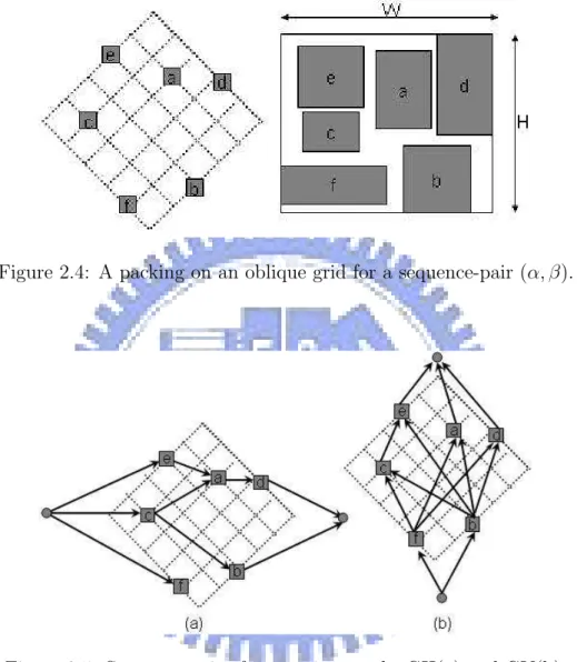
(18) Figure 2.2: The pair consisting of A block and B block are arranged symmetrically on a common axis [32].. Figure 2.3: Three resistor pairs which are arranged in an interdigitated fashion with one dimensional common-centroid symmetry.. 2.1.2. Sequence-pair placement method. Sequence-pair representation which is used in placement was proposed by Murata and Fujiyoshi[6]. This is a pair comprising module-name sequence such as (ecadfb,fcbead),where a,b,c,d,e,f represents the modules for packing. These two sequences represents the relationship between two blocks as follows: (...a...b...),(...a...b...):means ”a” is on the left of ”b” (...b...a...),(...a...b...):means ”b” is below of ”a” From the sequence-pair, we can convert it into the oblique grid graph. Figure 2.4 shows the grid and the corresponding packing. From this grid graph, we can de6.
(19) termine the approximate location of each module and construct a horizontal graph and a vertical graph, as shown in Figure 2.5.. Figure 2.4: A packing on an oblique grid for a sequence-pair (α, β).. Figure 2.5: Sequence-pair of constraint graph: GH(a) and GV(b).. Consequently, given sequence pair is (α, β); the horizontal relationship among blocks follows a horizontal constraint graph GH(V,E), which can be constructed as follows: 1) V:source s, sink t, and m vertices labeled with module names 2) E:(s,x) and (x,t) for each module x, and (x,x’) if and only if x is left of constraint 3) Vertex weight equals the width of block m, but zero for source(s) and sink(t). The vertical constraint graph GV(V,E) can be similarly constructed. Both GH(V,E) 7.
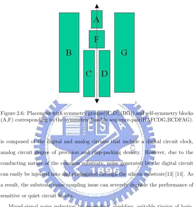
(20) and GV(V,E) are vertex-weighted directed acyclic graphs, so they can be applied to determine the x and y coordinates of each block by using the longest path algorithm.. 2.1.3. Placement of symmetry constraints with sequencepair method. The problem of symmetry constraints was studied by [8][12]. Let (α, β) be the sequence-pair of a placement configuration containing a few symmetry groups ( each group is composed of pair of symmetric blocks, and self-symmetric blocks which are relative to a common vertical axis). The position of block A in α and β sequences −1 is denoted by αA and βA−1 and define by y = sym(x) the block y symmetric to x.. if for any distinct blocks x,y in any of the symmetry groups satisfy:. αx−1 < αy−1 ⇔ β −1 sym(y) < β −1 sym(x). (2.1). This is called the symmetric-feasible in this sequence-pair (α, β). Any two selfsymmetric blocks in the some symmetry group appear in reversed order in the two sequences of the encoding. For example, Figure 2.6 shows a placement corresponding to the sequence-pair (BAFCDG,BCDFAG). It assumes a symmetry group composed of two symmetric pairs (C,D) (B,G) and two self-symmetric blocks A and F, according to EQ(2.1), the sequence-pair is symmetric-feasible. It can effectively define symmetric groups which are relative to a common vertical axis. For the common horizontal axis, this is similar to the vertical axis.. 2.2. SOC design for substrate noise issues and solutions. Continued scaling of the CMOS process, smaller size, and more features have motivated the combining of analog circuits with digital system. The mixed-signal chip 8.
(21) Figure 2.6: Placement with symmetry groups((C,D),(BG)) and self-symmetry blocks (A,F) corresponding to the symmetric-feasible sequence-pair(BAFCDG,BCDFAG).. is composed of the digital and analog circuits that include a digital circuit clock, analog circuit degree of precision and chip-packing density. However, due to the conducting nature of the common substrate, noise generated by the digital circuit can easily be injected into and propagated through the silicon substrate[13] [14]. As a result, the substrate noise coupling issue can severely degrade the performance of sensitive or quiet circuit blocks. Mixed-signal noise reduction by grounding, shielding, suitable timing of logic, signal routing, and power distribution has been discussed. These techniques may be broadly classified as discussed in [15]: 1) Reducing Noise Source Strength: To prevent unnecessary switching currents, logic drivers that are not in use should be shutdown. And high switching logic circuits, such as static CMOS, that require large transient current which lead to the generation of more switching noise, should be avoided. There have been many studies on this issue, such as current mode logic (CML) circuit, emitter coupled logic(ECL), folded source-coupled logic(FSCL)[16] 9.
(22) [17], and enhancement source-coupled logic (ESCL)[18]. 2) Reduction of Simultaneous Switching Noise: Output drivers that switch simultaneously generate noise and disturb the operation of gates that are connected to the same power-supply network. In order to alleviate the phenomenon, two different methods are proposed: current-controlled(CC), and controlled slew rate(CSR) output drivers[19]. The second approach uses distributed and weighted switching driver segments to control the slew rate of the output driver for a given load capacitance, and uses an additional damping resistor in the output driver circuit to reduce the power-supply network noise. Another technique, TCMOS [20] is also proposed, in which power is provided to the digital circuits through a controlled current injector stage which has the ability to isolate the main power supply bus from the noise power networks of the digital circuits. Therefore, a tank capacitor to store sufficient energy is necessary for the TCMOS technique. 3) Decoupling bypassing technique for RLC power-supply networks: In order to have a stable voltage of power-supply, the off-chip and on-chip decoupling capacitances need to be inserted into the power-supply networks. These capacitors act as filter circuits for low and high frequency components of the noise, in order to reduce fluctuations due to switching noise current spikes or voltage drop. 4) Reducing substrate noise interference to quiet circuits: To reduce the coupling from the aggressor logic circuits to the victim analog circuits on a high resistivity substrate, it is necessary to separate the chip powersupply networks of the noisy (aggressor) and quiet (victim) circuits if possible [21]. The substrate doping density and the distance between aggressor and victim blocks determine the impedance path between noise and quiet circuit blocks. The signal coupling from the two blocks is a function of this impedance, which should be used to minimize noise coupling. This can be achieved by decreasing the doping density. 10.
(23) Figure 2.7: Device simulation results for peak-to-peak noise as a function of distance between digital noise source and current source [22].. or increasing the distance, but it is also necessary to prevent the latch-up issue. Figure 2.7 shows device simulation results for the dependence of peak-to-peak noise on the distance between a current source transistor and an equivalent drain diffusion [22]. Noise voltage decreases almost linearly with separation in a lightly doped substrate. But in a heavily doped substrate, because of small path impedance, the injected noise current flows almost directly down through the noise contact into the substrate and then up through to the analog circuit devices. For this kind of substrate type, which requires increasing the distance between the noise and quite block, the noise signal is not an effective method for reducing substrate noise coupling. Therefore a mixed-signal design, using a lightly doped substrate, is a better approach than using a heavily doped substrate. 5) Guard Ring isolation solution for noise reduction: Guard Ring is one of the most used isolation schemes, and appear to be best suited for preventing crosstalk at high operational frequencies [23] . The guard ring 11.
(24) Figure 2.8: Effect of various guard ring structures by device simulation [22].. is connected to a fixed supply voltage around the circuit (analog or digital block circuits) by absorbing the potential substrate fluctuations. In other words, it is regarded as a low impedance path to a quiet potential, therefore flattening the noise voltage by reducing the noise before it reaches the protected blocks. Figure 2.8 shows the device simulation result for the variations of guard ring structure [22]. The simulation results show that a p+ guard ring structure can reduce the switching noise by almost an order of magnitude, because a p+ guard ring structure acts as a current sink that keeps the substrate quiet in the immediate vicinity of the current source. But in heavily doped structure, a n-well guard diffusion without p+ channel stop implant has almost no effect because most of the substrate current flows into the heavily doped bulk and not into the p+ channel stop diffusion near to the die surface. Another approach is shown in Figure 2.9(a). Dielectric trench oxide around the p+ guard ring [23] is used. Generally, trenches are lined with a dielectric and filled. 12.
(25) Figure 2.9: (a)Dielectric trench oxide around p+ guard rings. Normally, trenches are lined with a dielectric and filled with polysilicon [23]. (b) SOI CMOS devices dielectrically isolated from one another [24],[25]. (c) triple-well structure where in analog and digital CMOS circuits are each formed inside deep p-well regions that are separated by n-type substrate regions [24].. with polysilicon. A second approach, the SOI process, is also suggested to reduce noise crosstalk. Figure 2.9 (b) shows CMOS devices isolated by using buried oxide matter that seqarates them from each other. We can also use triple-well structure to suppress noise coupling [24]. In this process, each of the analog and digital devices are separately formed inside deep p-well regions in a common n-substrate, as shown in Figure 2.9(c).. 2.3. Decoupling capacitance allocation for powersupply noise suppression. The trend of increasing power and clock frequency while reducing power supply voltage causes IR drop and Ldi/dt noise over the power supply network. This will introduce logic failure, reduce noise margins and reduce the reliability of high. 13.
(26) performance chips. To solve the problem, decoupling capacitors are often added in order to keep power supply within specification. Figure 2.10 shows the RLC power-supply network [26]. Each of the mesh grids is seen as a block function which includes the current source, the power line is equivalent to the lumped RLC element. According to [26], the noise calculation of each module can use Kirchhoff’s voltage law to represent as follows: (k). Vnoise =. X. (ij RP jk + LP jk. P j∈T (k). dij ) dt. (2.2). (k). where Vnoise denotes the power supply noise at module(block) K, P j denotes the path from VDD to node j, Pjk denotes the path from node j to node k, T (k) denotes the resistance of Pjk , LP jk denotes the inductance of Pjk and ij is the current flowing along path P j.. Figure 2.10: Model of power-supply network [26].. 14.
(27) 2.4. Problem formulation. Given n rectangular analog blocks including k symmetry groups and m rectangular digital blocks including j noise blocks. Each symmetry group of analog blocks is composed of pairs of symmetry blocks and/or self-symmetry blocks. All of the blocks have its height hi and width wj, and digital blocks have its average current for considering the blocks noise and decap budget estimation. To use two-phase method for our SOC floorplan. The objective of first-phase is to find a floorplan with minimal analog blocks area. The objective of second-phase is to find a floorplan with minimal digital blocks noise interference to analog blocks, and the minimal power drop voltage with a suitable decap budget. The resultant chip area can be minimal under the condition that all blocks are not allowed to be overlapped.. 15.
(28) Chapter 3 Mixed-Signal chip floorplanning with symmetry constraint and substrate noise consideration We use two-phase method to implement the mixed-signal floorplanning which proceed in three steps. The first step concerns the analog blocks. Considering the blocks with symmetry constraints, we use symmetric-feasible sequence-pairs to obtain the floorplanning result. We will improve the approach in [12] to constructed symmetric blocks with sequence-pair. The second step considering digital blocks with noise-aware analog blocks. The weights of noise-aware contain process parameters, blink magnitude of current factor which decide distance relation of digital and analog blocks. The third step, we insert suitable Decap budget according to EQ(2.2). We use an annealing algorithm to carry out all of the blocks’ floorplan process. The objective is to construct a floorplan with minimal digital block noise interference to analog block and minimal voltage drop by adding suitable decap budget.. 16.
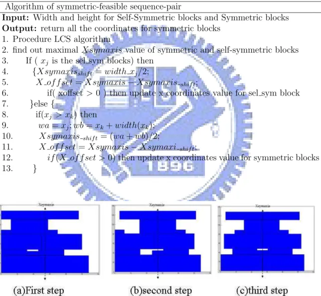
(29) 3.1. Symmetric-Feasible sequence-pairs for analog placement. In sequence-pairs packing we will improve the method with the fast evaluation of sequence-pairs proposed by [12]. We use EQ(2.1) and the LCS [27] method to achieve symmetric-Feasible packing for analog blocks. The computation of symmetric-feasible properties can be performed in three parts. The LCS algorithm is the first part, the input sequence-pair is (α, β) and defined by the blocks as 1,2,...n and the weight w(b) is equal to the width of block b. P[b] is defined by block position array, b=1,2...n is used to record the x coordinate of block b. The array match[i], i=1,2...n is constructed for X[i]=Y[j]. i.e., match[i]=j if and only if X[i]=Y[j]. The length array L[1...n] is used to record the length of candidates of the LCS. The algorithm is in Figure 3.1. The second part is to find out the maximal x coordinate value of symmetric. Figure 3.1: The packing of sequence-pairs using the LCS algorithm [27].. and self-symmetric blocks. For instance: Xsymaxis = max(xj + (xk + width xk )/2) ,where xj < xk and j, k is any index pair of symmetric or self-symmetric block, and following this step, we use the LCS algorithm again to update the x coordinate. In 17.
(30) the third part, we need to move some symmetric blocks to the Xsymaxis axis. The algorithm is shown below. Figure 3.2 summarizes the three parts for symmetricfeasible sequence-pairs. We also allow for rotation of the symmetry group. The algorithm is similar to the above description; we only swap the sequence-pair (α, β) and reverse the index of α sequence. Figure 3.3 is an example for the result of a symmetric group. Algorithm of symmetric-feasible sequence-pair Input: Width and height for Self-Symmetric blocks and Symmetric blocks Output: return all the coordinates for symmetric blocks 1. Procedure LCS algorithm 2. find out maximal Xsymaxis value of symmetric and self-symmetric blocks 3. If ( xj is the sel sym blocks) then 4. {Xsymaxisshif t = width xj /2; 5. X of f set = Xsymaxis − Xsymaxis shif t ; 6. if( xoffset > 0 ) then update x coordinates value for sel sym block 7. }else { 8. if(xj > xk ) then 9. wa = xj ; wb = xk + width(xk ); 10. Xsymaxis shif t = (wa + wb)/2; 11. X of f set = Xsymaxis − Xsymaxi shif t ; 12. if (X of f set > 0) then update x coordinates value for symmetric blocks 13. }. Figure 3.2: The Summary of the three parts for symmetric-feasible sequence-pairs.. 18.
(31) Figure 3.3: An example for the result of a symmetric group.. 3.2. Substrate noise coupling model for mixed-signal chip. Based on vertical process-dependent factors, the substrate carries many R-C parasitic elements because of well-capacitances and high-low(p/n) junctions. Figure 3.4 shows the simulation model for a chip of substrate [15]. However, for a two-port device, we can combine R-C networks together to two ports of the y-parameters model [14]. This is shown in Figure 3.5(a). In terms of circuit elements, the twoport y parameters can be written as: µ ¶ y11 (ω) y12 (ω) y(w) = y21 (ω) Y22 (ω). (3.1). where y(ω) = g(ω) + jωC(ω) and y12 (ω) = y21 (ω). This model is seen as frequencydependent. However, according to [14], we simulate the relationship with frequency and impedance of the two-port model. From Figure 3.6 we can know that it is seen the impedance constant nearly in 10G Hz. Therefore it can be regarded as pure resistance model as Figure 3.5(b).. 3.2.1. Substrate coupling model simulation result. We use the model in Figure 3.5(a) to simulate noise coupling effect between clock generator and LNA (Low Noise Amplifier) circuit. Figure 3.7 illustrates our simulation method, to include aggressor (clock generator), victim (signal amplifier) 19.
(32) Figure 3.4: Simulation model for chip of substrate [15].. Figure 3.5: (a) Substrate model for frequency-dependent y-parameters [14]. (b) Substrate model of pure resistance [28].. and a common substrate model. Since the noise magnitude of aggressor and victim blocks is a function of impedance [29] [13], as shown Table (3.1), we input a plus wave of 0.1V into the analog block and defing LNA gain as 6. Table (3.1) shows the noise peak voltage is decreasing when the distance between aggressor and victim blocks is increasing. Based on the EQ(3.2) that is proposed by [29], where dij is the distance between two points; si and sj are the areas of contact i and contact j; pi and pj are the perimeters of contact i and j; α1, α2, α3 and β depend on fundry process; we can know that Rij has a relationship with the foundry process and distance between two. 20.
(33) Table 3.1: Substrate noise between aggressor and victim block of distance Opa Vout(peck voltage). Sub Noise (peck voltage). Resistance value(Y12). 1.0808 0.77446 0.60742 0.59584 0.58712 0.58409 0.57674 0.57615 0.57514 0.57369. 0.51091 0.20543 0.054866 0.02893 0.01937 0.014812 0.0099055 0.0074657 0.0060376 0.004982. 77 1k 5k 10k 15k 20k 30k 40k 50k 60k. Figure 3.6: Substrate mode simulations for y11, y12, y22 impedance. blocks. Rij = β • [ln(dij + 1)]α1 • (sj + sj )α2 • (pi + pj )α3 ]. (3.2). To simplify the computation, we define a weight called ’α’, which depends on clock frequency, current density and the foundry process. The EQ(3.2) is formulated as follows:. Rij =. α · ln(. p (x1 − x2 )2 + (y1 − y2 )2 ) √ √ W+ L. (3.3). Where x1 , x2 , y1 , y2 are the coordinates of the victim block and aggressor block; W , L are the contact dimension, and α is the curve fitting coefficient. In [29], the substrate noise isolation between aggressor and victim block is defined as: Isolation Rate = 20 log(victim/aggressor)(db). 21. (3.4).
(34) Figure 3.7: Using substrate model to simulate noise coupling effect between clock generator and LNA circuit (a) Three blocks including aggressor (clock generator), victim (signal amplifier), and a common substrate model. (b) Clock generator. (c) LNA circuit.. We will follow the noise model of Section 3.2 and EQ(3.3) to determine the magnitude of victim block noise in relation to aggressor block noise. Finally, the constraint of noise-aware analog blocks for digital block (x,y) coordinates can be resolved by EQ(3.4).. 3.3. Decoupling capacitance allocation by using the insertion and area-sizing method. According to [30], the power-supply drop and ground bounce is related to risetime, falling-time of the clock, drive loads, and power-supply. The is shown in Figure 3.8 and EQ(3.5) and (3.6) as follows:. 22.
(35) Figure 3.8: Test circuit of power and ground bounce [30]. s Vg(max) = Vk +. K2 + Lg K3 (1 − Lg K1. 1+. 2Lg K1 Vk ) K2 + L g K3. (3.5). 1+. 2Lp K1 Vk ) K2 + Lp K3. (3.6). s Vp(max). K2 + Lp K3 (1 − = Vk + Lp K1. In EQ(3.5)(3.6), we can know that rise-time and fall-time are the main factors which influence power-supply drop. Therefore, for reason of explanation, we have assumed some parameters for convenience of computation and simulation. Figure 3.9 (a) shows our simulation circuit. We use a 0.18um mixed-signal process model, with vdd = 3.3V , rise/falling time=0.01us, and package inductance=5nH. The waveform is shown in Figure 3.9 (b), and drop voltage on the power line is 2.78V. We use C = Q/V = 122nF to compute the capacitance budget. The waveform of adding decap device is shown in Figure 3.9 (c), and the drop voltage on the power line is 3.28v. In our placement, we will use EQ(2.2) in Section 2.3 to define constraint limit of the power-supply drop voltage, and then will insert some appropriate decap 23.
(36) budget to restrict the amount of voltage dropping. Moreover, for area constraint of the blocks placement, we implement two approaches: area sizing of decap blocks and insertion. In order to minimize the final floorplan area during the decap allocation, dimension of blocks should be sized to control whole area of chip. If this cannot satisfy the constraint of the final chip area, an insertion approach will be used by decap allocation (The chip area is greater than 2% when decap use area sizing approach). This is shown in Figure 3.10 (a) and (b); the decap device should be placed as close as possible to the noise blocks to minimize the magnitude of power-supply voltage drop. Figure 3.9 (d) shows the waveform after dispersion the Decap to near the noise circuit, the drop voltage on the power line is 3.22V, decap=60nF.. 3.4. Annealing process in block placement. We employ the following set of moves by using LCS algorithm [27]. We perturb the sequence-pair to obtain a new sequence-pair during simulating annealing. The perturbation continues to search for a good configuration until a predefined termination condition is satisfied.. 3.4.1. Dealing with blocks sets of the moves. 1) Swapping two symmetry-pairs blocks of the same symmetry group: Two symmetry-pairs blocks are picked randomly and swapped in a horizontal or vertical direction. Figure 3.11 illustrates an example: horizontal swap: S1 , S2 = (...A1 , B1 ..., B2 , A2 ) ⇔ S1 , S2 = (...B1 , A1 ..., A2 , B2 ) vertical swap: S1 = (...A1 , A2 ..., B1 , B2 ...), S2 = (...B1 , B2 ..., A1 , A2 ...) ⇔ S1 = (...B1 , B2 ..., A1 , A2 ...), S2 = 24.
(37) Figure 3.9: To simulate power-supply drop and ground bounce effect (a) Voltage drop test circuit of power-supply. (b) Waveform before decap allocation. (c) Waveform after decap allocation. (d) Waveform after dispersion to near the noise circuit.. 25.
(38) Figure 3.10: (a)Area sizing of noise block. (b)Insertion approach for the decap device.. (...A1 , A2 ..., B1 , B2 ...) 2) Swapping two symmetry groups: Two symmetry groups are picked randomly and swapped. Each symmetry group is treated as one block, these block coordinates of each symmetry group will be shifted based on symmetry group coordinates. 3) Rotating a symmetry group: A symmetry group is picked randomly and its orientation is changed from horizontal or vertical, in Section 3.1, Figure 3.3 shows this example. 4) Swapping two cells: Two blocks for asymmetric or symmetry groups are picked randomly and swapped. The elements of sequence-pairs S1 , S2 can be exchanged, but the relative orderings between blocks of the same group are not changed. 5) Exchange the width and height of a block (rotate a block): A block is picked randomly and its width and height are changed. If a block which belongs to a symmetry pair is rotated, it must also correspond the third condition. 6) Preplace a block: Some noise blocks must be pre-placed prior to the annealing process; these blocks may overlap other blocks. Therefore, it needs to check the conflict during dealing. 26.
(39) Figure 3.11: Swapping two symmetry-pairs blocks of the same symmetry group.. blocks with sets of moves. We define dx, dy and bx, by are the radius of the block and the distance of the center coordinates between two blocks. Figure 3.12 illustrates the example: if bx < (dx1 + dx2) and by < (dy1 + dy2), then two blocks are overlap together.. 3.4.2. Annealing process in mixed-signal blocks. Figure 3.13 illustrates our floorplan design flow of MS-SOC blocks. We divide the annealing process into three parts. The first part, in analog blocks, is to minimize the cost function of every symmetry group and non-symmetric blocks. These blocks are applied to the set of moves in Section 3.4.1 and are to minimizing the area size. We use symmetric-feasible sequence-pairs approach to process placement, and it is much faster than the LP-programming approach [8] [31]. In the next chapter, we will present our experimental results, proving that it is possible to obtain a more efficent solution than [8] [31] in the same benchmark. In the second part, analog blocks are seen as pre-place blocks and digital blocks are used to minimize the cost function including noise-aware analog blocks. We 27.
(40) Figure 3.12: dx, dy and bx, by are the radius of the block and the distance of the center coordinates between two blocks.. apply the method in Section 3.2, and each noise weight of noise blocks is used to reduce the analog blocks interference and to minimize the chip size in the annealing process. In the third part we apply the method in Section 3.3 for insertion of appropriate decap device in final floorplanning. The objective is to minimize the power-supply drop voltage. Incidentally, the decap device can also help to reduce the substrate noise coupling issue [15]. Since the power-supply drop and substrate noise are mostly caused by clock switching or buffer driver of high current.. 28.
(41) Figure 3.13: Mixed-Signal chip floorplanning design flow. Using two-phase method to process the analog blocks and digital blocks separately. This flow divides the annealing process into three parts. The first part is to pack analog blocks, the second part is to pack digital blocks with noise blocks which use substrate noise model. Finally, we insert appropriate decaps in the floorplan.. 29.
(42) Chapter 4 Experimental results In this section, in order to compare our results with [9] [10], we present our results in two parts: analog and mixed-signal blocks. Since there are no other similar mixed-signal works we can compare, we propose two approaches in order to present our experimental results of mixed-signal placement. In the analog placement part, we use the Symmetric-Feasible sequence-pair method to implement our algorithm. This approach is more effective for obtaining large-scale block placement satisfying the given symmetry constraints. We use benchmarks in [9] (D50 D70 D100 D120 D170 D220) to test our floorplan. For each experiment, the initial temperature is set to 7 ∗ 104 , and the cost function defined as: cost(F )=area(F )+α*wire(F ), where F is the floorplan, area(F ) is the total area of executed blocks, α is a user given weight, and wire(F ) is the total wire length of F measured by the half-perimeter estimation. Table 4.1 shows the experimental results. In Table 4.1, we compare the dead space, chip area and time cost with [9] [10]. We implemented our algorithm in the C++ programming language in Intel Pentium4 3.0G/1G Memory. It shows that our Symmetric-Feasible sequence-pair method is more effective when the total numbers of blocks are increased. Table 4.2 shows the comparison of results with [9] in Intel CPU Q6600-2.40GHz/2G Memory on Linux System, this machine is compatible with [9]. For each experiment, the initial temperature is set to 45 ∗ 104 . When the number of blocks is increased to 30.
(43) Table 4.1: We use benchmarks in [9] to test analog blocks floorplan. Experimental comparisons between the results of our approach and [9][10]. Data Set. Our approach Area. D50 D70 D100 D120 D170 D220. 17640 19782 44304 46060 65534 90100. Dead space 0.124 0.152 0.152 0.146 0.164 0.147. Time (min) 1.81 2.11 2.86 4.56 8.08 10.2. [10] Area 20153.1 20750.6 53793.2 46115.3 67605.6 91560. [9]. Dead space 0.234 0.1921 0.302 0.147 0.19 0.16. Time (min) 3.3 3.4 4.3 5.9 11.1 12.7. Area 23834 25497 58289 57817 73595 101535. Dead space 0.35 0.34 0.35 0.32 0.25 0.24. Time(s) 65 128.4 288 399 790 1230. Table 4.2: We use benchmarks in [9] to test analog blocks floorplan. Experimental comparisons between the results of our approach and [9] on Linux System. Data Set. D50 D70 D100 D120 D170 D220. Our approach Area Dead Time(s) space 18207 0.15 102 19404 0.13 122 44270 0.15 142 43575 0.09 151 60515 0.09 134 85248 0.09 130. Area 18576 22575 45540 49126 ——-. [9] Dead space 0.17 0.26 0.18 0.20 ——-. Time(s) 100.4 212.5 475.4 510.3 ——-. 220, we will have a smaller dead space in our algorithm than [9] and [10]. Figure 4.1 shows an example for the results of analog floorplan with 220 analog blocks include 5 symmetric groups.. In the mixed-signal placement part, for the noise-aware issue we have developed two methods to present our results. In the first method (Compulsory pre-placed noise blocks approach), all of the noise blocks will first be pre-placed in order to correspond with noise constraint cost; then the LCS algorithm will check overlap for pre-placed blocks and other blocks. If these blocks are overlapped, the coordinates of blocks will be moved to avoid any overlap constraint. In the second method (Elastic pre-placed noise blocks approach), all of the digital blocks will be placed directly by using the LCS algorithm; then we will check the noise blocks whether they cor-. 31.
(44) Figure 4.1: An example of experimental result of 220 analog blocks include 5 symmetric groups. respond with noise constraint cost. If there are any noise blocks that violate noise constraint cost, these blocks will be moved to another position in order to meet the noise constraint. Finally, we will update those blocks in the order of sequence-pairs. In order to miminize power and substrate noise issue, high noise blocks possibly are not abutment together in the floorplan. Table 4.3 shows the experimental results. For each experiment, the initial temperature is set to 70∗104 , 540 digital block and cost function defined as: cost(F )=area(F )+ α*wire(F ) + β*noise violations. The noise violations are set to −25db; α, β are a user given weight, area(F ) is the total area of executed blocks and wire(F ) is the total wire length of F measured by half-perimeter estimation. In the method two, we will have a smaller dead space, cost time and decap-budget than method one. Table 4.4 shows another set of experimental results. We assign 5, 10 and 20 noise blocks. In Method Two, we also obtain better results than in Method One. Figure 4.2 shows an example for the results of mixed-signal floorplan with 540 digital and. 32.
(45) 120 analog blocks.. Table 4.3: Using 540 digital blocks include 10 noise blocks to test our floorplan alogrithm in different analog blocks. Experimental comparisons between the Method One(Compulsory pre-placed noise blocks approach) and Method Two(Elastic preplaced noise blocks approach) which use 540 digital blocks, 10 noise blocks. Data Set. Method one Area. D50 D70 D100 D120 D170 D220. 681210 679294 704759 700848 718773 764975. Dead space 0.15 0.14 0.14 0.14 0.14 0.16. isolation rate(db) -27.36 -27.1 -26.9 -27.1 -26.6 -26.5. Method two Decap (uF) 1.72 1.76 1.63 1.68 1.73 1.7. Time(s) Area 561 562 561 564 564 565. 650496 652365 678436 674707 703917 730730. Dead space 0.11 0.11 0.11 0.10 0.12 0.12. isolation rate(db) -27 -27 -26.5 -26.7 -26.8 -26.9. Decap (uF) 1.69 1.67 1.69 1.65 1.70 1.7. Time(s) 549 550 551 552 551 569. Table 4.4: Using 540 digital blocks and 120 analog blocks to test our floorplan algorithm in different noise blocks. Experimental comparisons between the Method One and Method Two (540 digital blocks, 120 analog blocks). Noise block N.O. Method one. Area 5 10 20 25 30. 692640 700848 729300 799200 941752. Dead space 0.13 0.14 0.17 0.24 0.35. isolation rate(db) -27 -27.1 -26.8 -26.7 -26.7. Method two. Decap (uF) 1.74 1.7 1.65 1.7 1.75. Time(s) Area 540 563 747 1187 1444. 33. 685386 674707 684618 687675 684743. Dead space 0.12 0.10 0.12 0.12 0.11. isolation rate(db) -27.3 -26.7 -27 -26.8 -26.8. Decap (uF) 1.65 1.65 1.65 1.75 1.75. Time(s) 541 552 571 586 592.
(46) Figure 4.2: An Example of experimental results of mixed-signal placement with 540 digital and 120 analog blocks.. 34.
(47) Chapter 5 Conclusion and future work We have presented some approaches for handling the placement of MS-SOC physical design. The method for analog blocks packing is based on sequence-pairs by Longest Common Subsequence (LCS) algorithm and simulated annealing. We extend this algorithm to handle symmetry placement of analog blocks, so that it can be used to place very large-scale SOC designs circuit that may contain thousands of analog and digital blocks of various sizes. During the annealing process it also considers the noise-aware problem by using substrate nouise coupling model so that the interference of the noise blocks to the sensitive analog blocks can be minimized. Our future work will focus on the placement of analog blocks. We also need to consider passive components such as: resistor and capacitor elements. Moreover, wire routing of analog blocks for symmetry blocks is an important factor, since it also relates to the noise immunity ability. Investigation of methods for handling symmetry-wire routing of the symmetry blocks is also a very important area of research.. 35.
(48) Bibliography [1] Shiyou Zhao, Kaushik Roy, and Cheng-Kok Koh. “Estimation of inductive and resistive switching noise on power supply network in deep sub-micron CMOS circuits.” In IEEE/ACM International Conference on ComputerAided Design, pp. 65-72, Sept. 2000. [2] J. Cohn, D. Garrod, R. Rutenbar, and L. Carly. “Analog Device-Level Layout Automation.” Kluwer Academic Publication, 1994. [3] Florin Balasa, Sarat C.Maruvada, and Karthik Krishnamoorthy. “Efficient solution space exploration based on segment trees in analog placement for analog placement with symmetry constraints.” In IEEE/ACM International Conference on Computer-Aided Design, pp 497-502, Nov. 2002. [4] Yun-Chih Chang, Yao-Wen Chang, Guang-Ming Wu, and Shu-Wei Wu. “B*trees: a new representation for nonslicing floorplans.” In IEEE/ACM International Conference on Computer-Aided Design, pp. 458-463, 2000. [5] P. N. Guo, G. K. Chen, and T. Yoshimura. “An O-tree representation of nonslicing floorplan and its application.” In IEEE/ACM International Conference on Computer-Aided Design, pp. 268-273, 1999. [6] Hiroshi Murata, Kunihiro Fujiyoushi, Shigetoshi Nakatake, and Yoji Kajitani. “Rectangle-Packing-Based module placement.” In IEEE/ACM International Conference on Computer-Aided Design, pp. 472-479, Nov. 1995. 36.
(49) [7] Jai-Ming Lin and Yao-Wen Chang. “TCG: A transitive closure graph-based representation for nonslicing floorplans.” In IEEE/ACM International Conference on Computer-Aided Design, pp. 764-769, 2001. [8] Florin Balasa and Koen Lampaert. “Symmetry within the sequence-pair representation in the context of placement for analog design.” In IEEE/ACM International Conference on Computer-Aided Design, pp. 721-731, July. 2000. [9] Yiu-Cheong Tam, Evangeline F.Y. Young, and Chris Chu. “Analog placement with symmetry and other placement constraints.” In IEEE/ACM International Conference on Computer-Aided Design, pp. 349-354, Nov. 2006. [10] Hsin-Wen Fang and Hung-Ming Chen. “An algorithm for Large-Scale analog block placement with symmetry constraints.” National Chiao Tung University Thesis, 2007. [11] Sujoy Mitra, Rob A. Rutenbar, L. Richard Carley, and David J. Allstot. “Substrate-aware mixed-signal macrocell placement in WRIGHT.” In IEEE Journal Solid-State Circuits Conference, pp. 269-278, Mar. 1995. [12] Karthik Krishnamoorthy, Sarat C. Maruvada, and Florin Balasa. “Fast evaluation of symmetric-feasible sequence-pairs for analog topological placement.” In IEEE/ACM International Conference on Computer-Aided Design, pp. 71-74, Oct. 2003. [13] Brian E. Owens, Sirisha Adluri, Patrick Birrer, Robert Shreeve, Sasi Kumar Arunachalam, and Kartikeya Mayaram. “Simulation and measurement of supply and substrate noise in mixed-signal ICs.” In IEEE Journal SolidState Circuits Conference, pp. 382-391, Feb. 2005. [14] Hai Lan, Zhiping Yu, and Robert W. Dutton. “A CAD-Oriented modeling approach of frequency-dependent behavior of substrate noise coupling 37.
(50) for mixed-signal IC design.” In IEEE International Symposium on Quality Electronic Design, pp. 195-200, March. 2003. [15] Ali Afzali-Kusha, and Nishath K. Verghese. “Substrate noise coupling in SOC design:Modeling, Avoidance, and Validation.” In Proceedings IEEE/ACM International Conference on Computer-Aided Design, pp. 21092138, Dec. 2006. [16] David J. Allstot, San-Hwa Chee, Sayfe Kiaei, and Manu Shrivastawa. “Folded source-coupled logic vs. CMOS static logic for low-noise mixedsignal ICs.” In IEEE International Conference on Electronics, Circuits, and Systems, pp. 553-563, Sep. 1993. [17] Sailesh R. Maskai, Sayfe Kiaei, and David J. Allstot. “Synthesis techniques for CMOS folded source-coupled logic circuits.” In IEEE Journal Solid-State Circuits Conference, pp. 1157-1167, Aug 1992. [18] M. Maleki and S. Kiaei. “Enhancement source-coupled logic for mixed-mode VLSI circuits.” In IEEE transactions on Circuits and Systems, vol. 39, pp. 399-402, Jun 1992. [19] R. Senthinathan and J. L. Prince. “Application specific CMOS output driver circuit design techniques to reduce simultaneous switching noise.” In IEEE Journal Solid-State Circuits Conference, pp. 1383-1388, Dec. 1993. [20] J. L. Gonzalez and A. Rubio. “TCMOS: Low noise power supply technique for digital ICs.” In IEEE Journal Electronics Letters, vol. 31, pp. 1338-1339, Aug. 1995. [21] B. Nauta and G. Hoogzaad. “How to deal with substrate noise in analog CMOS circuits.” In IEEE Proceedings Europe Conference Circuits Theory Designs, pp. 121-126, 1997. 38.
(51) [22] David K. Su, Marc J. Loinaz, Shoichi Masui, and Brunce A. Wooley. “Experimental results and modeling techniques for substrate noise in mixed-signal integrated circuits.” In IEEE Journal Solid-State Circuits Conference, pp. 420-430, Apr. 1993. [23] Kuntal Joardar. “A simple approach to modeling cross-talk in integrated circuits.” In IEEE Journal Solid-State Circuits Conference, pp. 1212-1219, Oct. 1994. [24] Tsukada Toshiro and Fukuda Keiko Makie. “Approaches to reducing digitalnoise coupling in CMOS mixed-signal LSIs.” IEICE Transactions on fundamentals of Electronics, Communications Computer Sciences, vol E80-A, pp. 263-275, Feb. 1997. [25] J. P. Colinge, J. P. Eggermont, D. Flandre, P. Francis, and P. G. A. Jespers. “Potential of SOI for analog and mixed analog-digital low-power applications.” In IEEE Journal Solid-State Circuits Conference, pp. 194-195, Feb 1995. [26] Shiyou Zhao, Kaushik Roy, and Cheng-Kok Koh. “Decoupling capacitance Allocation and its application to power-supply noise-aware floorplanning.” In IEEE/ACM International Conference on Computer-Aided Design, pp. 81-92, Jan. 2002. [27] Xiaoping Tang, Ruiqi Tian, and D. F. Wong. “Fast evaluation of sequence pair in block placement by Longest Common Subsequence computation.” In IEEE/ACM International Conference on Computer-Aided Design, pp. 521526,. Yokohama,Japan, Jan. 2001. [28] Minsik Cho, Hongjoonh Shin, and David Z. Pan. “Fast substrate noiseaware floorplanning with preference directed graph for mixed-signal SOCs.” 39.
(52) In IEEE/ACM Asia and South Pacific Design Automation Conference, pp. 24-27, Jan. 2006. [29] HaiLan, Tze Wee Chen, Chi On Chui, Parastoo Nikaeen, Jae Wook Kim, and Robert W.Dutton. “Synthesized compact models and experimental verifications for substrate noise coupling in mixed-signal ICs.” In IEEE Journal Solid-State Circuits Conference, pp. 1817-1829, Aug. 2006. [30] Adnan Kabbani and Asim J. Al-Khalili. “Estimation of ground bounce effects on CMOS circuits.” In IEEE International Symposium on Circuits and Systems, pp. 533-536, vol. 22, June. 1999. [31] Shinichi Kouda, Chikaaki Kodama, and Kunihiro Fujiyoshi. “Improved method of cell placement with symmetry constraints for analog IC layout design.” In Portal International Symposium on Physical Design, pp. 192199, April. 2006. [32] Alan Hastings and Roy Alan Hastings. “The Art of Analog Layout,” Prentice Hall Publication, 2001. [33] Chao-Hung Lu, Hung-Ming Chen, and Chien-Nan Jimmy Liu. “On increasing signal integrity with minimal decap insertion in area-array SOC floorplan design.” In IEEE Asia and South Pacific Design Automation Conference, pp. 792-797, Jan. 2007.. 40.
(53)
數據

![Figure 2.2: The pair consisting of A block and B block are arranged symmetrically on a common axis [32].](https://thumb-ap.123doks.com/thumbv2/9libinfo/8382116.178241/18.892.306.587.154.385/figure-pair-consisting-block-block-arranged-symmetrically-common.webp)
+7
![Figure 2.7: Device simulation results for peak-to-peak noise as a function of distance between digital noise source and current source [22].](https://thumb-ap.123doks.com/thumbv2/9libinfo/8382116.178241/23.892.124.772.153.827/figure-device-simulation-results-function-distance-digital-current.webp)
![Figure 2.8: Effect of various guard ring structures by device simulation [22].](https://thumb-ap.123doks.com/thumbv2/9libinfo/8382116.178241/24.892.126.779.155.824/figure-effect-various-guard-ring-structures-device-simulation.webp)
![Figure 2.10: Model of power-supply network [26].](https://thumb-ap.123doks.com/thumbv2/9libinfo/8382116.178241/26.892.125.767.367.1011/figure-model-of-power-supply-network.webp)
![Figure 3.1: The packing of sequence-pairs using the LCS algorithm [27].](https://thumb-ap.123doks.com/thumbv2/9libinfo/8382116.178241/29.892.129.771.413.934/figure-packing-sequence-pairs-using-lcs-algorithm.webp)
相關文件
You are given the wavelength and total energy of a light pulse and asked to find the number of photons it
Wang, Solving pseudomonotone variational inequalities and pseudocon- vex optimization problems using the projection neural network, IEEE Transactions on Neural Networks 17
volume suppressed mass: (TeV) 2 /M P ∼ 10 −4 eV → mm range can be experimentally tested for any number of extra dimensions - Light U(1) gauge bosons: no derivative couplings. =>
Define instead the imaginary.. potential, magnetic field, lattice…) Dirac-BdG Hamiltonian:. with small, and matrix
incapable to extract any quantities from QCD, nor to tackle the most interesting physics, namely, the spontaneously chiral symmetry breaking and the color confinement..
• Formation of massive primordial stars as origin of objects in the early universe. • Supernova explosions might be visible to the most
2-1 註冊為會員後您便有了個別的”my iF”帳戶。完成註冊後請點選左方 Register entry (直接登入 my iF 則直接進入下方畫面),即可選擇目前開放可供參賽的獎項,找到iF STUDENT
For ex- ample, if every element in the image has the same colour, we expect the colour constancy sampler to pro- duce a very wide spread of samples for the surface
