利用殘餘應力組裝之讀寫頭Fresnel 透鏡
76
0
0
全文
(2) 利用殘餘應力組裝之讀寫頭 Fresnel 透鏡 Stress-induced Self-assembly of a Fresnel Lens for an Optical Pick-up Head. Student : Yi-Hsien Chen Advisor : Yi Chiu. 研 究 生 : 陳依纖 指導教授 : 邱一. 國立交通大學 電機資訊學院 電機與控制工程學系 碩士論文. A Thesis Submitted to Department of Electrical and Control Engineering College of Electrical Engineering and Computer Science National Chiao Tung University In Partial Fulfillment of the Requirement For the Degree of Master In Electrical and Control Engineering March 2005 Hsinchu, Taiwan, R.O. C. 中華民國九十四年三月.
(3) 中文摘要. 因為資訊技術(IT)的發展,對高速和高密度資料儲存的要求已經變得日益重 要,光學資料儲存系統正是其中一種可以滿足這種需求的裝置。對於微型化和質 量輕的要求推動了更輕更小的光學資料儲存系統的發展,而微光機電技術 (MOEMS)是製造更輕更小的光學資料儲存系統的方法之一。但在此微光機電領 域中,量產和自組裝是極重要的技術。如果量產和自組裝可實現,那這將使微光 機電技術能夠更容易和以更便宜的方法來生產微型化的光學讀取頭。此研究中, 設計了可以使微機電系統能夠被更容易和更便宜的方法來組裝直立元件的機構。 自組裝機構的發展使得微光學元件可以被自動組裝,但現今已開發出的數種 可用於組裝直立元件的裝置皆需額外的電熱能或製程。在本論文中的組裝直立元 件的機構,是利用製程中最後一道的金屬層本身的應力,設計出殘餘應力臂做為 自組裝的機構,來完成了自動組裝直立元件的動作。 此研究中欲組裝的元件為光學讀取頭中的聚焦元件。聚焦透鏡有兩種,一是 繞射式透鏡,另一種是折射式透鏡。每一種在光學方面都有它自己的優勢。在這 裡,所採用的是繞射式的 Fresnel 透鏡,因為 Fresnel 透鏡有孔徑大、薄和輕的優 點。輕薄的優點使得在這個系統中的這個結構能夠更容易的被殘餘應力臂抬起組 裝。 在許多研究中,討論利用各種不同材料來製作出 Fresnel 透鏡,例如:多晶 矽,AZ4620 等等。在本論文中,討論利用厚膜光阻 SU-8 製作出 Fresnel 透鏡, 因為厚膜光阻 SU-8 的材質對藍光雷射波長的吸收率極小,欲以此製作出極適用 於藍光雷射的 Fresnel 透鏡。. i.
(4) Abstract. Because of the progress of information technology (IT), the need for high speed and high density data storage has become increasingly important. The optical data storage system is one of the important devices for this need. The requirement of miniaturization and lightness pushes the development of more miniature and lighter optical data storage system. Micro Optical Electro Mechanical System (MOEMS) technology is one of methods to reach this target. If self-assembly of the MOEMS devices is realizable, it will make the technology an easier and cheaper way to produce the miniaturized pick-up head. It is important to exploit self-assembly mechanisms to assemble optical systems automatically. Until now, several methods have been developed to assemble the upright components, but extra electricity, heat or fabrication processing is needed. In this study, stress-induced beams are used to accomplish the self-assembly function to assemble a Fresnel lens. The tensile stress comes from the last metal layer in the process. The lens is the focusing component in a pick-up head. There are two kinds of lenses. One is diffractive lens, and the other is refractive. Each has its own advantage in optics. Here the diffractive lens – Fresnel lens is used because the Fresnel lens has several advantages such as much larger aperture, thin and light. The advantage of lightness makes it easier to flip up the lens structure by the stress-induced beam in this system. Different materials have been used to manufacture Fresnel lens. In this study, the thickness photoresist SU8 is adopted because the SU-8 has low absorption at blue laser wavelength.. ii.
(5) 誌謝 轉眼間研究所求學生涯來到了尾聲,一路走來,有幸邂逅了許多良師與益 友,給了許多的幫助與指導,使我能由原本的一無所知,到現在的完成本篇論文。 首先,要感謝的是我的指導教授邱一老師在研究上的指導與鼓勵,讓我能用 更嚴謹及努力不懈的態度來思考研究,並提供優良的研究環境讓我完成本篇論 文,也感謝各位口試委員所提供的寶貴意見,使本論文更加完善。 再者,在本論文的設計與實驗過程中,有幸得到了許許多多同學朋友的幫助 與寶貴建議,感謝這一路上幫助我的清大動機所、本校電子所、機械所、光電所 的各位學長與同學們,及奈米中心的技術人員先生小姐們,還有實驗室一起努力 的嘉豪及俊毅同學,學弟文中、英傑、育杉、志偉、炯廷、均宏、建勳及忠衛, 因為有你們,這段研究生活充滿了許多歡笑與美好的回憶。 對於我親愛的父母親及弟弟,感謝你們多年來對我的支持與鼓勵,讓我能無 後顧之憂的完成我的學業,謝謝你們。 最後,將此論文獻予我的父母、家人及所有曾幫助過我的人,我由衷的感激 大家對我的關懷與協助。. iii.
(6) Table of Content 中文摘要……………………………………………………………………………….i Abstract……..…………………………………………….…………...……………...ii 誌謝…………………………………………………..…..…………...........................iii Table of Content………………………………………………………..……………iv List of Figures…………………...……………………………………....…………...vi 1.Introduction………………………………………………………………………1 1-1 Motivation…………………………………..…....…………………………..1 1-2 Pick-up head……………………………………………….............................2 1-3 Self-assembly……………………………………………...............................4 1-4 Fresnel lens………………………………………………............................9 1-5 Thesis Overview………………………………………………....................14 2.Design and Analysis………………………………………………………….....15 2-1 Residual Stress Beam……………………………………………………….15 2-1.1 Analytical solution…………………………………………………..16 2-1.2 Simulation…………………………………………………………...18 2-1.3 Residual Stress Beam Design……………………………………….20 2-2 Fresnel lens………………….……………………………………………...21 2-3 Stress-induced self-assembly of a Fresnel lens……………….………….....25 3.Fabrication………………..………………………………..……………….……26 3-1 Fabrication Process………………………………………............................26 3-2 Fabrication Technology…….…………………………………………….....30 3-3 Problems and Discussions………………………………………………......33 4.Measurement…………………….……………………………….….………......39 4-1 MUMPs……………………………………………………………………..39 4-1.1 First MUMPs Run…………………………………………………...39 iv.
(7) 4-1.2 Second MUMPs Run………………………………………………..43 4-1.3 Discussions………………………………………………………….52 4-2 Fresnel lens……………………….………………………...……………....54 4-3 Stress-induced Self-assembly of a Fresnel lens……………...……………..60 5.Conclusion…………………….…………………………………………………..62 5-1 Conclusion….………………………………………………………………63 5-2 Future Work………………………………………………………………...63 6.Reference………………………………………………………………………...64. v.
(8) List of Figures Figure 1-1 Structure of a traditional optical pick-up head….………………………...2 Figure 1-2 SEM micrograph of the monolithic optical-disk pickup head…………….3 Figure 1-3 The detail of micro-optical pickup head…………………………………..3 Figure 1-4 Self-assembly by comb drive actuator and linear microvibromotor……...5 Figure 1-5 An automated assembly system connected to a scanning micromirror…...6 Figure 1-6 Self-assembled by SDA micromirror……………………………………..6 Figure 1-7 Self-assembled by photoresist…………………………………………….7 Figure 1-8 Optical switch assembled by stress-induced beam………………………..8 Figure 1-9 Fluidic self assembly……………………………………………………...8 Figure 1-10 Sequence of actuation. (a) Ultrasonic vibrations heat and charge the polysilicon parts. (b) Electrostatic repulsion forces the plate up………..9 Figure 1-11 Microlenses and their implementation………………………………….10 Figure 1-12 Schematic of an out-of-plane refractive microlens……………………..11 Figure 1-13 The blazing of a lens results in a reduced thickness……………………12 Figure 1-14 Schematic of (a) a continuous relief Fresnel zone plate, (b) a multiple-step level binary microlens…………………………………...13 Figure 1-15 The SEM of an out-of-plane binary Fresnel lens……………………….13 Figure 2-1 Two types of stress. (a) tensile Stress (b) compressive Stress…………...16 Figure 2-2 Dimensions of a cantilever beam………………………………………...17 Figure 2-3 Tip Deflection v.s. Beam Length………………………………………...19 Figure 2-4 The 3D distribution plot of the CoventorWare simulation result………..20 Figure 2-5 Residual stress beam. (a) with V shape (b) with funnel shape…………..21 Figure 2-6 The intensity profile and contour plot of the optical beam emitted from an optical fiber and collimated by the binary micro-Fresnel lens…………...22 Figure 2-7 Processing cycles of multi-level binary-optics microlens……………….23 vi.
(9) Figure 2-8 Fresnel lens. (a) 5mm focal length (b) 1cm focal length………………...24 Figure 2-9 Mask layout of stress-induced self-assembly of a Fresnel lens………….25 Figure 3-1 The layout diagram of stress-induced self-assembly Fresnel lens……….26 Figure 3-2 Cross sectional profiles are A-A’ and B-B’……………………………...27 Figure 3-3 Overetch………………………………………………………………….34 Figure 3-4 Without annealing………………………………………………………..34 Figure 3-5 With annealing…………………………………………………………...35 Figure 3-6 Wet etching patterned gold layer peels off………………………………35 Figure 3-7 Lift-off patterned gold layer sticks well…………………………………36 Figure 3-8 Plate with fissures………………………………………………………..36 Figure 3-9 The metal layer peels off………………………………………………...37 Figure 3-10 Releasing time is not enough…………………………………………...37 Figure 3-11 Releasing time is enough……………………………………………….38 Figure 4-1 First MUMPs run result………………………………………………….39 Figure 4-2 Magnified picture of a hinge…………………………………………….40 Figure 4-3 Layout and profile of the hinges………………………………………...40 Figure 4-4 Device1 measurement result…………………………………………….41 Figure 4-5 Device2 measurement result…………………………………………….42 Figure 4-6 Tip displacement of test beams in the first MUMPs run sample………..43 Figure 4-7 Vertical device1………………………………………………………….44 Figure 4-8 Side view of the vertical device1………………………………………...44 Figure 4-9 Curvature of the residual stress beam with the vertical plate…………....45 Figure 4-10 Curvature of the residual stress beam without vertical plate…………...45 Figure 4-11 Magnified picture of beam and plate…………………………………...46 Figure 4-12 An overview of the hinge group………………………………………..47 Figure 4-13 More than 90ْ device1………………………………………………….47 vii.
(10) Figure 4-14 (a) The hinge layout in this version (b) Hinge side view………………48 Figure 4-15 Vertical device2………………………………………………………...50 Figure 4-16 Side view of vertical device2…………………………………………..50 Figure 4-17 Magnified picture of one hinge in this hinge group……………………51 Figure 4-18 The end deflection of the beam in the device2…………………………51 Figure 4-19 The curves of every beam in the second MUMPs run………………….52 Figure 4-20 Distance between plate and beam………………………………………53 Figure 4-21 Hinge bar group in the not to be vertical device2………………………54 Figure 4-22 SU-8 Fresnel lens……………………………………………………….54 Figure 4-23 Magnified picture of the rings of the above lens……………………….55 Figure 4-24 5mm focal length Fresnel lens……………………………………...…..56 Figure 4-25 Part of the 5mm focal length Fresnel lens……………………………...56 Figure 4-26 The suface roughness of the central circle of the 5mm focal length Fresnel lens……………………………………………………………..57 Figure 4-27 Measurement and design data of the 5mm focal length Fresnel lens…..57 Figure 4-28 1cm focal length Fresnel lens…………….…………………………….58 Figure 4-29 Part of the 1cm focal length Fresnel lens……...………………………..59 Figure 4-30 The suface roughness of the central circle of the 1cm focal length Fresnel lens……………………………………………………………………..59 Figure 4-31 Measurement and design data of the 1cm focal length Fresnel lens…...60 Figure 4-32 (a) An overview of all devices (b) An overview of all devices…………………………………………60 Figure 4-33 Poly1 connected to poly2 in the hinge………………………………….61 Figure 4-34 Poly1 connected to poly2 between beam and plate…………………….62. viii.
(11) CHAPTER 1. Introduction 1-1 Motivation Because of the progress of information, the need of data storage is increasing to store the plentiful data such as software, music, movie and database. The explosive growth of data has produced a pressing need for large capacity data storage systems. Denser and faster data storage is needed, so the disk develops from CD to DVD. The DVD has a capacity of over seven times than CD. The pick-up head is one of the key components and has great influence on the performance in optical storage systems. Hence it is important to miniaturize and improve the performance of the pick-up head. To make the optical pick-up head by the MEMS technology is another solution to miniaturize and integrate the optical storage system. The greatest accomplishment of microelectromechanical systems (MEMS) is miniaturization, lightness and to produce mechanical motion on a small scale. Such mechanical devices are typically low power and fast, taking advantage of such micro scale phenomena as strong electrostatic forces and rapid thermal responses. MEMS-based sensors have been widely deployed and commercialized. MEMS technologies also show prospective applications in optics, transportation aerospace, robotics, chemical analysis systems, biotechnologies, medical engineering and microscopy using scanning micro probes [1]. And self-assembly technology is also an important issue for MEMS to assemble the whole system automatically instead of manually. 1.
(12) In this thesis, the research effort is directed at these two targets: 1. a self-assembled flip-up structure that can be used in an optical pick-up head to flip-up the Fresnel lens; 2. a Fresnel lens made by SU8.. 1-2 Pick-up head z. Traditional pick-up head. Figure 1-1: Structure of a traditional optical pick-up head Figure 1-1 is the structure of a traditional optical pick-up head. The pickup head is composed of a laser diode, a grating plate, a polarizing beam splitter, a collimator, a quarterwave plate, a mirror, an objective and photodiodes. The restriction of weight and volume causes traditional pickup head having difficulty on miniaturization. The need for high accuracy in assembly makes the traditional pickup head fabrication difficult and expensive. To develop the optical pick-up head that could be used in DVD and other disk devices by the MEMS technology is a method to solve these problems.. 2.
(13) z. MEMS pick-up head. Figure 1-2: SEM micrograph of the monolithic optical-disk pickup head [3]. Figure 1-2 is a single-chip optical-disk pickup head developed by M. C. Wu et al. [2]. The pickup head consists of a semiconductor laser source (hybrid integrated with the help of three-dimensional alignment plates), three micro-Fresnel lenses, a beam splitter, and two 45 degree mirrors.. Figure 1-3: The detail of micro-optical pickup head The micro-optical MEMS pickup head of this research is composed of a laser diode, a coupling and beam shaping lens, a grating plate, a beam splitter, a focusing 3.
(14) lens, focusing actuators and photodiodes as shown in Figure 1-3. All the optical elements are prealigned during the design stage. That differs from the manual alignment in traditional pickup head fabrication processes. The optical beam emitted by the laser is first collimated by the first microlens (the coupling and beam shaping lens).Then the horizontal beam is reflected by the 45ْ mirror to be a vertical beam, finally through the objective to be focused on the disk. The returned light is collected by the same microlens, reflected by the beam splitter, and focused onto the photodiode detectors on the silicon substrate to get the data. In this thesis, the Fresnel lens is used for coupling, shaping and focusing in the system, and the residual stress beams are used to flip-up the Fresnel lens structure.. 1-3. Self-assembly Because MEMS components are too small to assemble manually or by. traditional machines, it is necessary to exploitation a technology to assemble the devices. Here, the assembly technologies that are particularly used for optical applications will be described. z. By Microactuators Many surface-micromachined microactuators have been proposed, demonstrated. and integrated with the optical elements. On-chip actuators are used for the micromachined components to function in a self-contained optical module. 1). Comb drive actuator and linear microvibromotor:. Each of the two sliders is actuated with an integrated microvibromotor, which consists of four electrostatic-comb resonators with attached impact arms driving a slider through oblique impact. The complete structure is composed of two sets of vibromotors to drive the front and rear sliders for actuation of the mirror, as shown in. 4.
(15) Figure 1-4 [4].. Support beam. Slider Comb resonator. Mirror. Figure 1-4: Self-assembly by comb drive actuator and linear microvibromotor 2). Thermal actuator and microengine:. This example is called a linear assembly motor as shown in Figure 1-5 [5]. The system consists of three distinct parts: a linear assembly motor consisting of a drive actuator array (a), a coupling actuator array (b), and a drive arm (c); a vertical actuator (d); and a self-engaging locking mechanism (e). The system is connected to a scanning micromirror (f). The linear assembly motor utilizes two arrays of lateral thermal actuators to move a drive arm. One actuator array serves to couple and decouple the motion of the drive actuators from the drive arm. Cycling the drive array through two positions and selectively coupling the drive yoke with the drive arm result in a motion of the drive arm in one direction. The direction can be reversed by changing the cycle of the coupling array relative to the cycle of the drive array.. 5.
(16) Figure 1-5: An automated assembly system connected to a scanning micromirror 3). Scratch drive actuator (SDA):. When SDAs are employed as microactuators, the moving distance of the translation stage is mainly determined by the traveling distance of the SDAs. The SDA travels until it hits the stop block on the substrate. The most reliable way is to make a stop block with vertical side walls and without affecting the flatness of the underlying silicon nitride layer. As the pushrod is rotated up, the hinge pin starts to touch the hinge staple when the mirror angle approaches 90ْ (pushrod angle 70ْ ). The pressure from the hinge staple presses the hinge pin down and backward, thus preventing it from sliding. A structure that is self-assembled by SDA is shown in Figure 1-6 [6].. Figure 1-6: Self-assembled by SDA micromirror 6.
(17) From the above surveys, microactuators can not assemble a batch of devices at the same time. This is not a good way to assemble piece by piece with extra actuators, spending a lot of time, die area, manpower and money. It is impossible to batch process in the factory in the future. Due to the above reasons, low cost, automatic and economic solutions are surveyed below. z. By Surface Tension The devices are self-assembled by the out-of plane rotation due to the surface. tension torque obtained by melting thick pads of photoresist or solder. The fabrication processes are to pattern device first, and then pattern the photoresist or put solder on the rotation joints and melt them. The plate will flip up following by the surface tension power during melting the photoresist or solder. The final angle of the flip-up structure can be controlled accurately by simple mechanisms based on the layout stage. An example of assembled by photoresist is shown in Figure 1-7 [7].. photoresist. Figure 1-7: Self-assembled by photoresist z. By Residual Stress Residual stress makes a bimorph beam bend, and it can be used to lift the. structure up. The detail of residual stress beam is described in Section 2-1. Figure 1-8 [8] shows an example of self-assembled by stress-induced beams. The mirror arrays are assembled by stress-induced beams produced by Lucent Technology. 7.
(18) Stress beam. Figure 1-8: Optical switch assembled by stress-induced beam z. By Fluidic Self Assembly (FSA) Fluidic self assembly is a technique for accurately assembling large numbers of. very small devices. Fluidic self assembly starts with the micromachining of the objects to be self assembled, and target sites which have a matching shape. The surfaces are treated to control surface forces, and the objects are transported in liquid slurry. In the assembly process, a carrier fluid transports the objects over the target substrate, and when a binding site on a objects interacts with a receptor site on the substrate, there is a certain probability of attachment. If the object does not “fall” in the target well, it is carried away by the fluid and may be transported to another site. Through this process, devices eventually occupy all of the substrate sites. Figure 1-9 [9] is the model of fluidic self assembly.. Figure 1-9: Fluidic self assembly 8.
(19) z. By Ultrasonic Triboelectricity This is a method for batch assembly of polysilicon hinged structures. This. method uses ultrasonic vibrations generated with an attached piezoelectric actuator to vibrate polysilicon plates on silicon nitride or polysilicon surfaces. The rubbing between the substrate and the structures creates contact electrification charge that results in plates flapped to be stabilized vertically on the substrate at elevated temperatures. The charge repulsion effectively stabilizes the surface micromachined flaps to the upright position and nearly perfect yield over the entire area can be achieved. Figure 1-10 [10] shows the sequence of actuation by ultrasonic triboelectricity.. Figure 1-10: Sequence of actuation. (a) Ultrasonic vibrations heat and charge the polysilicon parts. (b) Electrostatic repulsion forces the plate up. After surveying the assembly methods, the residual stress beam is the choice of this thesis to assemble the Fresnel lens device vertically. The residual stress beams are not only used to flip up the structure but also for positioning. After designing suitable positioning structure, the offset of the assembled plate can be remarkably reduced.. 1-4 Fresnel lens There are three kinds of focusing microlenses. One is refractive microlenses, one. 9.
(20) is reflective microlenses, and another common focusing microoptical element is diffractive microlenses, as shown in Figure 1-11 [11]. The diffractive microlens will be researched in this thesis because it is the thinnest and lightest.. Figure 1-11: Microlenses and their implementation z. Refractive Microlenses The focal length of refractive microlens is independent of the optical wavelength. (except a weak dependence due to the dispersion of the lens material). It is also easier to make fast refractive microlenses without tight critical dimension control. Refractive microlens is easier to manufacture at low cost. Fabrication of a planar refractive microlens array on semiconductor and dielectric substrates has been demonstrated using photoresist/polyimide reflow techniques. The lens pattern can also be transferred to substrate through reactive ion etching [12] or ion milling [13]. Fig. 1-12 shows the schematic drawing of the out-of-plane refractive spherical lens [14]. Here, surface-micromachining processes are employed in the planar refractive microlens fabrication to create low-cost, high-quality out-of-plane refractive microlenses. But one potential issue of such lens to be used in our system is too heavy to assemble.. 10.
(21) Figure 1-12: Schematic of an out-of-plane refractive microlens z. Diffractive Microlenses Diffractive optics can be viewed as an approach to the fabrication of optical. components optimized for the application of photolithography techniques. In refractive optical elements (ROEs), the light is manipulated by analog phase elements of considerable thickness (in relation to the optical wavelength). The refractive optical elements whose diameters are tens to hundreds of micrometers and phase structures are thickness > 10µm are necessary. For optimized components, the solution is to lie in the periodic nature of the light wave U(x). If a light wave is delayed by one wavelength (corresponding to a phase lag of φ=2π), no difference to the original wave can be found Eq. (1-1). U(x, φ) = A0(x) eiφ = A0(x) eiφ+2π = U(x, φ+2π). (1-1). Ratardation occurs, for example, when the wave passes through a dielectric material (e.g., glass or photoresist). The insensitivity of the light wave to phase jumps of N·2π (N: integer) allows one to reduce the thickness of an optical element without changing its effect on a monochromatic wave, as shown in Figure 1-13. In transmission the maximum thickness of the corresponding optical component can be reduced to tmax=λ/(n-1), where n denotes the refractive index of the component material and λ is the wavelength of the incidence light. 11.
(22) Figure 1-13: The blazing of a lens results in a reduced thickness. Diffractive microlenses are very attractive for integrating with free-space microoptical bench (FS-MOB) because: 1) their focal length can be precisely defined by photolithography; 2) microlenses with a wide range of numerical apertures (F/0.3–F/5) can be defined; 3) microlenses with diameters as small as a few tens of micrometers can be made; 4) their thickness is on the order of an optical wavelength. The thin construction is particularly suitable for the surface micromachining process because the thicknesses of the structural layers are only on the order of 1 µm. There are two kinds of diffractive microlenses, one is the continuous kinoform lens, and the other is the approximation of the kinoform lens. The continuous kinoform relief lens can be made by direct laser writing in photoresist or patterned by gray scale mask shown in Figure 1-14(a) [3]. The approximate kinoform lens can be made by multiple-step process of binary-optical design. That is made advantage of that multiple-step level binary microlens is easy to fabricate. Figure 1-14 (b) is the schematic diagrams of a multiple-step level binary microlens.. Figure 1-14: Schematic of (a) a continuous relief Fresnel zone plate, (b) a multiple-step level binary microlens. 12.
(23) The binary Fresnel zone plate has alternating transmission and blocking zones. Though it is very easy to fabricate, however, its efficiency (diffraction efficiency into the first-order beam) is limited to 10%. The efficiency of a binary microlens with M = 2m step levels is. ⎡ sin( π /M) ⎤ η= ⎢⎣ π /M ⎥⎦. 2. The efficiency increases with the number of step levels at the expense of more complicated fabrication processes. For example, η= 41% for M=2, η= 81% for M=4, and η= 99% for M=16. Fabrication of binary microlenses on various substrates has already been demonstrated. Fig. 1-15 [3] shows the SEM micrograph of a binary micro-Fresnel lens which is made by one binary mask step.. Figure 1-15: The SEM of an out-of-plane binary Fresnel lens The weight of diffractive lens is lighter than the refractive lens. In this thesis, a Fresnel zone plate lens is used because the strength of the stress-induced beam is limited. The material for the Fresnel lens is SU-8 because SU-8 has low absorption at blue laser wavelength.. 13.
(24) 1-5 Thesis Overview The objectives of this thesis are: (a) To develop a set of stress induced beams that can be used to flip up the structure plate. The residual stress beams flip up and position the structure plate to be vertical from the substrate. (b) To develop a binary Fresnel lens that is set in the flipped up plate. The binary Fresnel lens is constructed by the photoresist of SU-8. The fundamental principles of the residual stress beams and the binary Fresnel zone plate lenses are described in detail in Chapter 2. The fabrication process and process issues are described in Chapter 3. The experiment results and discussion are presented in Chapter 4. Conclusions and future works are discussed in Chapter 5.. 14.
(25) CHAPTER 2. Design and Analysis The basic structure of the self-assembled Fresnel lens by stress induced beams is composed of two residual stress beams and a Fresnel lens made of photoresist or SU-8. In this chapter, the design and analysis of the residual stress beam and the SU-8 Fresnel lens are discussed.. 2-1 Residual Stress Beam Stresses in deposited thin films can have serious effects on the properties, performance, and long term stability of the device. Developments in the fabrication of freestanding micromechanical structures using surface micromachining techniques require knowledge of and control over the internal stresses. Residual stress can be divided into thermal stress and intrinsic stress according to its source. The formula of the thermal stress is shown in Eq.2-1. σth = E∆α∆T. (2-1). where E is the elastic coefficient, ∆α is the difference in coefficients of thermal expansion coefficient between the film and the substrate and ∆T is the difference between the deposition temperature and the room temperature. If the temperature of the fabrication is higher, the main stress is produced by thermal stress. The intrinsic stress, σi, reflects the internal structure of a material and is less clearly understood than the thermal stress, which it often dominates. Several phenomena may contribute to σi, making its analysis very complex. Intrinsic stress 15.
(26) depends on thickness, deposition rate (locking in defects), deposition temperature, ambient pressure, method of film preparation, type of substrate used (lattice mismatch), incorporation of impurities during growth, etc. The types of stress in the films are separated into two kinds, one is tensile stress, and the other is compressive stress. In bimorph beams, the upper layer that has a tensile stress and the lower layer that has zero stress make the cantilever beam to curve upwards, as shown in Figure 2-1(a). If the upper layer has a compressive stress and the lower layer has zero stress, they make the cantilever beam bow downwards, as shown in Figure 2-1(b). Excessive compressive or tensile strain fields result in splintering, cracking and adhesion problems of the film to the substrate.. Figure 2-1: Two types of stress. (a) tensile Stress (b) compressive Stress Stress is a serious problem in surface micromachining. But here the drawback is transferred to be an advantage to apply a force to pop up the structure. In this thesis, the residual stress beams are used to supply the force to lift up the plate of the Fresnel lens. The theory and calculation of the lift up height of the stress-induced beam will be discussed.. 2-1.1. Analytical solution. The cantilever becomes curved from the bending moment caused by the variation in stress between the upper and lower films. The beam bends upward because the lower film has a compressive residual stress while the upper film has a tensile residual stress. The curvature of the cantilever and the maximum beam 16.
(27) deflection are determined by the physical dimensions and material properties. The dimension parameters of a cantilever beam are labeled in Figure 2-2 [15].. Figure 2-2: Dimensions of a cantilever beam When two films of different residual stresses share an interface at equilibrium, the induced forces P1 and P2, and the moments M1 and M2, must be balanced [16]:. P1 = P2 = P P⋅. h = M1 + M 2 = M , 2. (2-2). where h = h1 +h2 is the total thickness of the beam. To Calculate the moment-curvature relations for each material, an equivalent beam strength (EI). equiv. can be defined [17], [18], ( E ⋅ I ) equiv. where. E 2 ⋅ b ⋅ h23 = ⋅K, 12(1 + m ⋅ n). (2-3). K=1+4mn+6mn2+4mn3+m2n4 m=. E1 h and n = 1 E2 h2. (2-4). and E1 and E2 are the Young’s modulus and h1 and h2 are the thicknesses of the lower film and the upper film, respectively. The relationship between the stress-induced internal force (P) and the radius of curvature (ρ) can be determined: P=. 2 ⋅ ( E ⋅ I ) equiv h⋅ρ. (2-5). The radius of curvature (ρ) is constant along the beam, since the internal force (P) and the beam geometry do not vary. An additional condition is that of zero slip at the interface. The strain in each. 17.
(28) film is composed of three components: one due to the residual stresses σ1 and σ2, one due to the axial force P, and one due to the curvature ρ of the beam. Setting the sum of the three components in one material equal to that of the other at the interface is that:. σ1 E1. +. h σ h p P + 1 = 2 − − 2 E1 h1b 2 ρ E 2 E 2 h2 b 2 ρ. (2-6). The radius of curvature of the pre-biased flexure is obtained by solving Eqs. (2-3), (2-5) and (2-6), 1. ρ. =. 6( m ⋅ σ 2 − σ 1 ) h ⋅ E 2 (3m + K [n(1 + n) 2 ] −1 ). (2-7). With the radius of curvature known, the end deflection of the beam can be calculated from trigonometry. The deflection perpendicular to the unreleased position for a given beam length, L, with radius of curvature ρ is given by. δ = ρ (1 − cos( L / ρ )). 2-1.2. (2-8). Simulation. The bending height of the bimorph residual stress beam is calculated by utilizing the above theory and simulated by Coventorware. The material and geometric parameter of a Si3N4/Poly-Si bimorph are E1 = 161Gpa (polysilicon), E2 = 270Gpa (silicon nitride) [19], h1 = 2µm, h2 = 0.5µm, σ1 = 0Mpa and σ2 = 100Mpa. The material and geometric parameter of a Gold/Poly-Si bimorph are E1 = 161Gpa (polysilicon), E2 = 78Gpa (gold) [19], h1 = 2µm, h2 = 0.5µm, σ1 = 0Mpa and σ2 = 270Mpa. The residual stresses are obtained from Ref [20] and measurement results. The deflection of a Si3N4/Poly-Si and a gold/Poly-Si residual stress beams, calculated from Eqs. (2-4) and (2-7), and of a Si3N4/Poly-Si residual stress beam, simulated by CoventorWare, is shown in Figure 2-3.. 18.
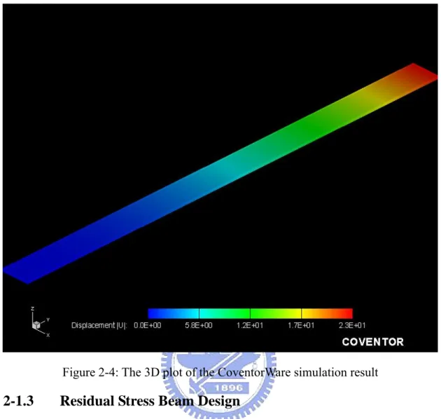
(29) Figure 2-3: Tip Deflection v.s. Beam Length Figure 2-4 is the 3D plot of the CoventorWare simulation result. The length and width of the beam are 750µm and 50µm, respectively. The beam is a Si3N4/Poly-Si bimorph. The thickness of Si3N4 and Poly layers are 0.5µm and 2µm, and the stress of Si3N4 and Poly layers are 100Mpa and zero, respectively. The simulation result of the end deflection to substrate is 23µm. From above calculation, the tip displacement of a 750µm long beam is 30µm. There is an error value between simulation result and calculation result. The error value is 23%. And because the Young’s modulus and residual stress can change with fabrication process, the calculation and simulation results are not the accurate values of the experiment result.. 19.
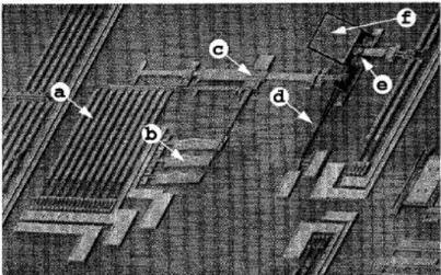
(30) Figure 2-4: The 3D plot of the CoventorWare simulation result. 2-1.3. Residual Stress Beam Design. The residual stress beams are the assemblers and the fixers in this system. Several residual stress beams are designed. There are ten different beam dimensions, two kinds of shapes in the tip and three different widths of necks in funnel shape, as shown in Figure 2-5. The beam dimensions are L × W = 500µm × 200µm, 500µm × 400µm, 500µm × 600µm, 700µm × 200µm, 700µm × 400µm, 700µm × 600µm, 1000µm × 200µm, 1000µm × 400µm, 1000µm × 600µm and 1000µm × 1000µm. The 1000µm × 1000µm is the limit of the residual stress beam dimension. The V and funnel shapes are two kinds of the beam tips to fix the device in after popping up. The widths of the neck in the funnel shape tips are 3µm, 5µm and 7µm. The total width of the neck is the 2µm thickness of the poly2 plate plus 1µm, 3µm or 5µm tolerance for the movement during 20.
(31) assembly. The residual stress beam is composed of two Poly layers and one residual stress layer. The Poly1 links with Poly2, and Poly1 area is under the Poly2 plate to pop up the plate. The residual stress layer is on the Poly2 layer.. W. Stress layer. L. Poly2. Poly1. (a). (b). Figure 2-5: Residual stress beam. (a) with V shape (b) with funnel shape. 2-2 Fresnel lens A diffractive microlens is a micro-optical component as small as a few tens of microns in diameter and with a thickness on the order of an optical wavelength. A binary diffractive microlens is an approximation of a kinoform, or continuous diffractive lens, designed by applying a phase-function constraint between 0 and 2π to subtract an integral number of wavelengths from the lens transmittance function. Theoretically, a kinoform lens has a 100% diffraction efficiency. The kinoform lens structure can be approximated by multilevel lithography and stepwise etching. 21.
(32) Figure 2-6: The intensity profile and contour plot of the optical beam emitted from an optical fiber and collimated by the binary micro-Fresnel lens. The binary lens also can exhibits very good optical performance. Figure 2-6 is an intensity profile and contour plot of the optical beam emitted from an optical fiber and collimated by the two-phase binary micro-Fresnel lens [21]. Very good agreement with Gaussian shape is obtained. The intensity full-width-at-half-maximum (FWHM) divergence angle of the collimated beam has been reduced from 5.0゚to 0.33゚. The diffraction efficiency of this two-phase micro-Fresnel lens was measured to be 8.6% [22]. This is in agreement with the theoretical limit of the binary Fresnel zone plate. Efficiency greater than 80% can be achieved by multilevel Fresnel lenses at the expense of more complicated fabrication processes. Another potential issue of fabricating diffractive optical elements on the surface micromachined polysilicon plates is the surface roughness. The plates might need to be smoothened by chemical mechanical planarization, which can reduce the surface roughness to 17 Å [23]. Figure 2-7 shows a processing cycle for fabrication of a binary-optics microlens. Figure 2-7(a), 2-7(b), and 2-7(c) illustrate the process of a two-phase, four-phase, and 22.
(33) eight-phase microlens.. Figure 2-7: Processing cycles of multi-level binary-optics microlens For a multi-level binary-optics structure, the etch depth of each level is defined by the relation [24]. d ( m) =. λ (n − 1)2 m. ,. (2-9). where λ is the light wavelength in free space, n is the index of refraction of the lens material, m is the mask number for the level-m process, and d(m) is the etch depth of the level m. An m-mask process produces an M=2m-step approximation to a continuous diffractive structure. Since microlenses operate over a small range in incident angle, a simple planar thin-film lens design is acceptable. The optical path difference (OPD) function for each lens is used to derive the following relationship among the zone radius, focal length, and wavelength [24]: r ( p, m) = [(. pλ 2 pλ 1 ) + 2 f ( m )] 2 m n2 n2. (2-10). where f is the focal length, p=0, 1, 2, 3… is the ring number, n is the refractive of the 23.
(34) substrate, and r(p, m) gives the successive zone radii for the patterns in mask number m. z. Fresnel lens Design. 1. 23456....... 1. (a). 2 34 5....... (b). Figure 2-8: Fresnel lens. (a) 5mm focal length (b) 1cm focal length In this study, the two-phase binary Fresnel lens is used. The odd annular rings are used in the mask design of this thesis. The following is the width of each ring of a 5mm focal length lens calculated from Eq. (2-10). Figure 2-8(a) is the layout of 5mm focal length Fresnel lens in accordance with those calculated values. The four bars in the lens support and link rings. The diameter of the first circle is 71.2µm. The widths of the other layout rings in turn are 14.7µm, 11.3µm, 9.5µm, 8.4µm, 7.6µm, 7.0µm, 6.5µm, 6.1µm, 5.8µm, 5.5µm, 5.2µm, 5.0µm, 4.8µm, 4.7µm, 4.5µm, 4.4µm, 4.3µm, 4.1µm, 4.0µm, 3.9µm. The following is the width of each ring of a 1cm focal length lens calculated from Eq. (2-10). Figure 2-8(b) is the layout of 1cm focal length Fresnel lens in accordance with those calculated values. The diameter of the first circle is 100.6µm. The widths of the other layout rings in turn are 20.8µm, 16.0µm, 13.5µm, 11.9µm, 10.7µm, 9.9µm, 9.2µm, 8.6µm, 8.2µm, 7.8µm. 24.
(35) 2-3. Stress-induced self-assembly of a Fresnel lens The stress-induced self-assembly of a Fresnel lens is composed of the residual. stress beam and Fresnel lens. Figure 2-9 is the mask layout. From the simulation in Section 2-1.2, the deflection height of the beam may be more than 100µm and the tip of the beam may hit the Fresnel lens. Two pop-up plates designed with different height. One is H=100µm, and the other is H=200µm. The layout of the plate is shown in Figure 2-9.. H. Figure 2-9: Mask layout of stress-induced self-assembly of a Fresnel lens. 25.
(36) CHAPTER 3. Fabrication Base on the design in Chapter 2, the fabrication processes and issues will be discussed.. 3-1 Fabrication Process Two fabrication processes are used to fabricate the device. The six-mask process is a standard process, and the five-mask process is a simplified process. The assembled plate in six-mask process is made by Poly2; but in five-mask process, the bottom of the assembled plate is made by the stress layer. The six-mask process is the major process in this thesis and will be described below. Figure 3-1 is the layout diagram of the stress-induced self-assembly Fresnel lens. Cross sectional profiles along A-A’ and B-B’ are shown in Figure 3-2. B. A. A’. B’. Figure 3-1: The layout diagram of stress-induced self-assembly Fresnel lens 26.
(37) A - A’. B - B’. 1. Deposit silicon dioxide by PECVD. 2. Etch silicon dioxide (to produce anchors by mask 1) by RIE. 3. Etch silicon dioxide (to produce dimples by mask 2) by RIE. 4. Deposit Poly1 by LPCVD. 5. Etch Poly1 (to produce patterns by mask 3) by RIE. Figure 3-2: Cross sectional profiles are A-A’ and B-B’.. 27.
(38) 6. Deposit silicon dioxide by PECVD. 7. Etch silicon dioxide (to produce patterns by mask4) by RIE. 8. Deposit Poly2 by LPCVD. 9. Etch Poly2 (to produce patterns by mask5) by RIE. 10. Deposit Si3N4 residual stress layer by LPCVD. Figure 3-2: (Continued). 28.
(39) 11. Etch Si3N4 residual stress layer (to produce patterns by mask6) by RIE. 12. Spin-coat and pattern SU8. 13. Etch sacrificial oxide. Figure 3-2: (Continued). z Process Flow Step1. Use the RCA method to clean the bare silicon wafers and start the fabrication process by growing the 2.0 um thick SiO2 film by PECVD. Step2. Lithographically pattern the 2.0 um thick SiO2 film for the anchor by RIE. Step3. Lithographically pattern with the dimples mask and the dimples are transferred into the SiO2 film by RIE. The depth of the dimples is 0.75 um. Step4. Deposit the first structural layer of low stress polysilicon (Poly1) with a thickness of 2.0 um by LPCVD and anneal the wafer at 1050゚C for 1 hour to reduce the stress in the Poly1 layer. Step5. Lithographically pattern the Poy1 for the first structural layer by RIE.. 29.
(40) Step6. Deposit a thickness of 2.0 um SiO2 layer by PECVD. Step7. Lithographically pattern the second 2.0 um thick SiO2 film for Poly1_Poly2_Via by RIE. Step8. Deposit the second structural layer of low stress polysilicon (Poly2) with a thickness of 1.5 um by LPCVD and anneal the wafer at 1050゚C for 1 hour to reduce the stress in the Poly2 layer. Step9. Lithographically pattern the Poy2 for the second structural layer by RIE. Step10. Deposit the final residual stress layer. Two kinds of materials are used in this thesis for the residual stress layer. In case of Si3N4, the stress layer is deposited by LPCVD. In case of gold, the stress layer is deposited by E-beam evaporation. Step11. Lithographically pattern the Si3N4 stress layer for the final residual stress layer by RIE. The gold stress layer is patterned by lift-off and does not require etching. Step12. Coat SU8 and lithographically pattern the final Fresnel lens. Step13. The structures are released by immersing the chips in a 49% HF solution followed by a CO2 drying process.. 3-2. Fabrication Technology In this section, the detail fabrication process technology is discussed. In the first step, on the RCA cleaned bare silicon wafer is deposited a 2.0µm. thickness SiO2 layer by PECVD. The deposition time of the 2.0µm SiO2 layer with 90sccm N2O and 5sccm SiH4 at 350℃, 400mTorr chamber pressure and 10W RF power is about 29 minutes. Then on the SiO2 layer is spin coated HMDS and a layer of thick photoresist. 30.
(41) AZ4620 as the etching mask for the subsequent oxide RIE for anchors. The minimum thickness of photoresist for etching 2.0µm thick SiO2 in RIE is 2.0µm. In this process, the thickness of photoresist is about 7.0µm. The spread cycle is 1000 rpm for 5 seconds. The spin cycle is 4500 rpm for 25 seconds. The temperature of soft bake is 90 ℃ for 3 minutes. The expose time is 2 to 2.5 minutes with the filter. AZ300 is used for AZ4620 development. The development time is 2 minutes, followed by a rinse in DI water. After exposing, developing and checking the pattern by an optical microscope, the hard bake is 120℃ for 10 minutes. If the pattern is not good, acetone is used for reworking. Next, the etching rate of RIE of the SiO2 layer grown by SiH4 and N2O is about 1000 Å per 30 seconds with the recipe of SF6 flow rate = 30sccm, CHF3 flow rate = 10sccm, pressure (p) = 50mTorr and 100W RF power. It takes 10 minutes to etch the thickness of 2.0µm SiO2. In this step, wet etching by B.O.E. is another choice. But the undercut is a problem which makes the pattern larger and sidewall not perfect. After the RIE, the photoresist is cleaned by H2SO4 : H2O2 =3 : 1. Then the dimple mask is patterned by FH6400 with spread cycle speed = 1000 rpm, spin cycle speed = 4000 rpm, soft bake time = 1.5 minutes, exposure time with filter = 42 seconds, development time = 20 seconds and hard bake time = 6 minutes. The thickness of photoresist is about 0.7µm. The 0.75µm dimples are etched by RIE for 3 minutes and 45 seconds with the same recipe as the anchor etch. After the etching step, the PR is removed by H2SO4 : H2O2 =3 : 1 . After etching the anchors and dimples, the thickness of 2.0µm poly1 is deposited by LPCVD. Before deposition, the wafer is cleaned by H2SO4 : H2O2 =3 : 1 for 15 minutes and dipped in B.O.E. for 1 to 3 minutes. Dipping the wafer in B.O.E. can clean the unnecessary SiO2 layer that is produced during cleaning. But dipping in B.O.E. makes the anchor pattern larger. Because the poly is the structure layer, the 31.
(42) stress is an important issue in this layer. Here the low stress poly is deposited by LPCVD for 400 minutes with the recipe of SiH4 flow rate = 40sccm, temperature (T) = 585 ℃, pressure (p) = 300mTorr and annealed at 1050℃ for 1 hour. To anneal all poly layers at the end also works. After depositing poly1, AZ4620 is spin coated with spread cycle speed = 1000 rpm for 5 seconds, spin cycle speed = 6000 rpm for 25 seconds, soft bake time = 3 minutes, exposure with filter time = 2 minutes, development time = 2 minutes and hard bake time = 10 minutes. The thickness is about 5µm, and the minimum thickness of photoresist used to etch 2.0µm thick poly1 in RIE is 2.0µm. Subsequently, the poly1 layer is etched by RIE for 8 minutes with the same recipe as etching the first SiO2 layer. After poly RIE, the second 2.0µm thick SiO2 layer is deposited by PECVD and patterned by RIE with the same recipe as the first one. Then the second 1.5µm thick poly layer is deposited by LPCVD for 300 minutes, annealed in furnace with N2 at 1050℃ for 1 hour, and then patterned by RIE for 6 minutes and 30 seconds with the same recipe as poly1. Before the deposition of the 1.5µm poly2, the wafer is cleaned and dipped in B.O.E. for 1 to 3 minutes. Next, two kinds of residual stress layers are used to produce the force to flip up the plate of lens: Si3N4 and gold. The Si3N4 is deposited by LPCVD with the recipe of NH3 flow rate = 105sccm, SiHCl2 flow rate = 35sccm, temperature = 800℃, pressure = 140mTorr. It takes 35 minutes to deposit the thickness of 0.35µm Si3N4 film. Before depositing, the initial clean and dipping in B.O.E. is necessary. Then on the Si3N4 film is spin coated FH6400 with the recipe of spread cycle speed = 1000rpm for 5 seconds, spin cycle speed = 3000 rpm for 25 seconds, soft bake time = 1 minute and 30 seconds, exposure time = 25 seconds, development time = 2 minutes. The nitride layer is then etched by RIE for 2 minutes with the same recipe 32.
(43) as etching SiO2 and poly. The gold layer (3000Å gold with 100Å Cr as the adhesion layer) is deposited by E-beam evaporation and patterned by lift-off. First, the wafer is coated with AZ5214E. Its side wall is sloped at a reentrant angle, which allows the metal to be deposited on the surfaces of the wafer and the photoresist, but provides breaks in the continuity of the metal over the reentrant photoresist step. The photoresist and unwanted metal (atop the photoresist) are then removed in the acetone bath. The recipe and steps of spin coating AZ5214E is spread cycle speed = 1000 rpm, spin cycle speed = 3500 rpm, soft bake time = 1.5 minutes, the first exposure time = 6 seconds, hard bake time = 2 minutes, the second exposure time = 57 seconds and development time in AZ300 = 30 seconds. The thickness of photoresist is about 1.7µm. Before metal deposition, the initial clean and dipping in B.O.E. is needed, too. Then the SU8 is spin coated with the recipe of spread cycle speed = 1000rpm for 5 seconds, spin cycle speed = 3000 rpm for 30 seconds, soft bake: step1. 65 ℃ for 1 minute and step2. 90 ℃ for 1 minute, exposure time = 5 seconds, post exposure bake time = 2 minutes in 90 ℃, development in SU8 developer = 1 minute, and hard bake = 6 minutes in 200 ℃. Finally, the sacrificial layer (SiO2) is etched by immersing the chips in a 49% HF or B.O.E. solution, and then the structure is released.. 3-3. Problems and Discussions In this section, the problems encountered during fabrication and solutions are. discussed. (1) Over etch. 33.
(44) The first SiO2 (anchor) layer is etched by poly RIE. Multiple etches are used to control the etching depth. The residual oxide thickness is etched by observing the color of the oxide layer using an optical microscope. Figure 3-3 shows a case where the oxide layer is overetched.. Overetch. Figure 3-3: Overetch (2) Annealing The anneal process is conducted after all poly layers are deposited. Figure 3-4 is the poly structure without annealing. The plate is curved. Figure 3-5 is another poly structure with annealing. The structure is flat.. Figure 3-4: Without annealing 34.
(45) Figure 3-5: With annealing (3) Gold adhesion Another problem in the process is the adhesion of gold. At first, the wet etching using 10%KI + 5%I2 + 85% H2O is used to pattern gold. Figure 3-6 shows that the gold layer peels off after wet etching. On the other hand, Figure 3-7 shows a gold layer patterned by lift-off. The gold layer sticks with the poly structure layer well.. Figure 3-6: Wet etching patterned gold layer peels off.. 35.
(46) Figure 3-7: Lift-off patterned gold layer sticks well. (4) Thermal stress Thermal stress is produced when pushing wafers into and pulling wafers out of the furnace. It can make the structure crack. Figure 3-8 shows the fissures that are produced by the thermal stress in the plate when the speed of pushing the wafer into the furnace is too fast. The problem can be avoided by pushing the wafer slowly.. Fissures. Figure 3-8: Plate with fissures (5) B.O.E. dipping The dipping process between deposition processes is very important to remove 36.
(47) the SiO2 on the top layer. In Figure 3-9, the 5000Å chromium (Cr) layer peeled off from the poly structure layer after releasing. The dipping time in Figure 3-9 is 1 minute in HF : H2O = 1 : 100. However, it was observed that after dipping Poly2 in B.O.E. for 3 minutes, the metal layer – 3000Å gold + 100Å chromium (Cr) bends the beam and still sticks to the beam perfectly.. Figure 3-9: The metal layer peels off. 6 Releasing time ○. In Figure 3-10, the SiO2 is not cleaned completely because of short releasing time (about 30 minutes). If the releasing time is long enough, the SiO2 is cleared after etching by B.O.E. for 2 hours, as shown in Figure 3-11.. SiO2. Figure 3-10: Releasing time is not enough. 37.
(48) Without SiO2. Figure 3-11: Releasing time is enough.. 38.
(49) CHAPTER 4. Measurement There are three main parts in this thesis. One is the plate self-assembled by residual stress beams, one is the Fresnel lens, and the other is the combination of those two parts to build a vertical Fresnel lens. In this chapter, the results of the three parts are discussed. In Section 4-1, two MUMPS samples are shown. In Section 4-2, a Fresnel lens experiment is shown. And finally, the result of the vertical Fresnel lenses is in Section 4-3.. 4-1 MUMPs Two Multi-User MEMS Processes (MUMPs) runs using gold-polysilicon stress beams were tested and the results are discussed.. 4-1.1. First MUMPs Run. Figure 4-1 shows the scanning electron microscopy (SEM) pictures of a device from the first MUMPs run sample. This figure is cut the unnecessary part. The lens plate can not be raised by stress induced beams successfully.. Figure 4-1: First MUMPs run result 39.
(50) Figure 4-2: Magnified picture of a hinge The cause of the failure to raise the lens plate is that the hinge bar is too wide to rotate in the staple, based on the MUMPs layout rules. As shown in Figure 4-2, the space under the staple for the hinge to rotate is too small.. Height = 4.75μm Width = 5μm Figure 4-3: Layout and profile of the hinges. 40.
(51) Figure 4-3 is the layout and profile of the hinges. The width of the hinge bar is 5µm, but the height of the staple is 4.75µm [(First Oxide=2.0µm) + (Poly1=2.0µm) + (Second Oxide=0.75µm) = 4.75µm]. The width of the hinge bar is wider than the inner space of the staple so the space for hinge rotating is not enough. The solution is to reduce the width of the hinge bar.. Height (Tip to substrate). Figure 4-4: Device1 measurement result There are two devices in the first run samples. In device1, the plate is 400 × 450 µm2 and the beams are 500 × 300 µm2. Figure 4-4 is the device1 measurement result by a WYKO interferometer. From the Y profile, the deflection is not due to the curvature of the plate caused by the residual stress. The deflection is the result from that the plate is flipped up by stress induced beams. The tip displacement of the 450 µm long plate composed of two structure layers (Poly1 and Poly2) is 55.0µm and the tip deflection angle is 7ْ .. 41.
(52) In device2, the plate is 400 × 550 µm2 and the beams are 800 × 400 µm2. Figure 4-5 is the device2 measurement result. From the X profile, the deflection is also caused of by the flip-up by stress induced beams. The tip displacement of the 550µm long plate composed of single structure layer (Poly2) is 55.6µm and the tip deflection angle is 5.8ْ .. Height (Tip to substrate). Figure 4-5: Device2 measurement result Figure 4-6 is the tip displacement of the test cantilever beams in this MUMPS die. From the run data in the MEMSCAP website, the thickness of Poly1 is about 2.0µm, the compressive stress in poly1 is 13MPa. The thickness of Poly2 is about 1.5 µm, and the compressive stress in poly2 is 18MPa. The thickness of gold is about 0.55µm, and the tensile stress in gold is 33MPa. The calculated curve of the cantilever beams based on the run data is also shown in Figure 4-6. The calculation result based on the run data is quite different from the experiment result. The other variable. 42.
(53) parameter, for example, Young’s modulus is needed to be measured and considered.. Figure 4-6: Tip displacement of test beams in the first MUMPs run sample In these two devices, the angle of device1 (length = 450µm) is larger than the angle of device2 (length = 550µm). From Chaper 2, a longer beam should have a larger bending height and tip deflection angle. From the measurement results, the longer stress beams do not raise the plate higher. The cause is that the longer beam is softer and has less actuation force.. 4-1.2. Second MUMPs Run. The second MUMPs sample is a modified version of the first one. The width of the hinge bar is reduced to 2µm. It is successful to assemble the plate to approach the vertical position by the residual stress beams. Two devices are tested in this sample. z. Device1. 43.
(54) Figure 4-7: Vertical device1. Figure 4-8: Side view of the vertical device1 Figure 4-7 is the SEM picture of the device whose residual stress beam length and width are 500µm and 300µm. The residual stress beam is composed of 1.5µm thickness Poly2 and 0.5µm thickness Gold. The length and width of the lens plate are 450µm and 400µm. The plate is composed of Poly1 and Poly2. This device is similar 44.
(55) to the first MUMPS version but the width of the hinge bar is reduced to 2µm and the shape of the beam tip is changed to a V-shape. Figure 4-8 is the side view of the SEM picture in Figure 4-10. The measured angle from Figure 4-8 by a protractor is about 90ْ .. Plate. Figure 4-9: Curvature of the residual stress beam with the vertical plate. Figure 4-10: Curvature of the residual stress beam without vertical plate 45.
(56) The curvature of the stress induced beam of this device is measured by WYKO, as shown in Figure 4-9. The end deflection perpendicular to the unreleased position is 43.0µm. The black area in front of the beam tip is the vertical plate. Figure 4-10 is the beam deflection perpendicular to the unreleased position without the plate. The end deflection height without the plate is 51.9µm. The height of the end deflection is larger than the beam with the plate. This result is caused by the fact that the plate touches and presses the residual stress beam, as shown in Figure 4-11.. Figure 4-11: Magnified picture of beam and plate Because there is no fixing mechanism in the design, the plate sways easily. The final angle of the plate is decided by the residual stress beams and the location of the hinge bar. Figures 4-12 shows the hinges in this vertical device. The 2µm wide hinge bar is located in the position that makes the plate vertical and fixed in the staple. If the hinge bar is not fixed, a swaying plate appears. Figure 4-13 is a swaying device and the rotation angle of the plate is more than 90ْ . 46.
(57) Figure 4-12: An overview of the hinge group. Figure 4-13: More than 90ْ device1 Next, the minimum rotation space for the hinge bar is discussed. Figure 4-14(a). 47.
(58) and (b) are the layout and side view of the hinge bar. The block A in Figure 4-14(b) is the rotation space of the hinge bar. The diagonal line (j) that is from the Poly2 layer to the Poly0 layer is the minimum.. Figure 4-14(a): The hinge layout in this version. 38.2Pْ. Block A. Figure 4-14(b): Hinge side view In Figure 4-14(b), the angle of the diagonal from the Poly2 layer to the Poly0 layer in the staple is 38.2ْ . The i is the height of the staple space, j is the 38.2ْ diagonal of the staple space, k is the 38.2ْ diagonal of Oxide1, l is the 38.2ْ diagonal of Oxide2, m is the 38.2ْ diagonal of Poly0, and n is the 38.2ْ diagonal of the hinge bar. 48.
(59) The height of staple space in this design is 2.75µm (2µm thickness Oxide1 + 0.75µm thickness Oxide2 = 2.75µm), as shown in Figure 4-17(b), and the length of the 38.2ْ diagonal of the space in the staple is 3.6µm {[The 38.2ْ diagonal of Oxide1 = 3.2µm (2µm × csc38.2ْ = 3.2µm)] + [The 38.2ْ diagonal of Oxide2 = 1.2µm (0.75µm × csc38.2ْ = 1.2µm)] – [The 38.2ْ diagonal of Poly0 = 0.8µm (0.5µm × csc38.2ْ = 0.8µm)] = 3.6µm}. The 45ْ diagonal of the hinge bar is 2.8µm (2µm × 2 = 2.8µm). The 38.2ْ diagonal of the staple space is larger than the 45ْ diagonal of the hinge bar. The redundant length is 0.8µm [(The 38.2ْ diagonal of the staple space = 3.6µm) – (The 45ْ diagonal of the hinge bar = 2.8µm) = 0.8µm]. Because the 38.2ْ diagonal of the staple space is larger than the 45ْ diagonal of the hinge bar, the plate can be rotated. If the layout of the block of Poly0 is changed, this space can be larger. If the location of the left Poly0 block is moved away from underneath the hinge bar, it will provide more space to rotate. The length of the 38.2ْ diagonal of the space will be 4.4µm {[The 38.2ْ diagonal of Oxide1 = 3.2µm (2µm × csc38.2ْ = 3.2µm)] + [The 38.2ْ diagonal of Oxide2 = 1.2µm (0.75µm × csc38.2ْ = 1.2µm)] = 4.4µm}. The redundant space is 1.6µm. z. Device2. Figure 4-15 is the SEM picture of a device with length and width of 800µm and 400µm, respectively. This device is readily assembled after releasing without CO2 drying. The stress beams and all the other components in this die are stuck on the substrate. This situation will be discussed in Section 4-1.3. Figure 4-16 is the side view SEM picture of Figure 4-20. The measured angle by a protractor is about 90.5ْ .. 49.
(60) Figure 4-15: Vertical device2. Figure 4-16: Side view of vertical device2 Figure 4-17 is the SEM picture of one hinge in this device. The hinge bar is about 1µm thick and slips into the space between staple and Poly0 and then be lodged in the space. The lodging in the space between staple and Poly0 fixes the angle and position 50.
(61) of the plate. The end deflection of this 800µm × 400µm beam is 140µm, as shown in Figure 4-18.. Figure 4-17: Magnified picture of one hinge in this hinge group. Figure 4-18: The end deflection of the beam in the device2 z. Test cantilever beams. There are test patterns in these dies to measure the residual stress. The type of the 51.
(62) stress in all gold stress beams is tensile. The radius of curvature of test cantilever beams is about 0.84mm. The curves of the test beams are plotted in Figure 4-19. The run data of MUMPs is that the thickness of Poly2 is about 1.58 µm, the thickness of gold is about 0.54µm, Poly2 has an 11MPa compressive stress and gold has a 24MPa tensile stress. From the curves in Figure 4-19, the measured data of all beams are quite different from the curve of MUMPs run data. The radius of curvature of the run data is about 7.5mm. The other variable parameter, for example, Young’s modulus is needed to be measured and considered.. Figure 4-19: The curves of every beam in the second MUMPs run. 4-1.3. Discussions. (1) Fixing mechanism Figure 4-20 is the magnified picture between plate and beam. From Figure 4-20, the distance between plate and beam is too wide to fix the plate in a fixed position. To 52.
(63) close plate and beam can improve the unstable problem. The funnel shape can also be used to improve this problem.. Figure 4-20: Distance between plate and beam. (2) Seized by staple Some devices are not flipped up to the vertical position because the hinge bar is seized in the staple too tightly to rotate the plate by residual stress beams, as shown in Figure 4-21. This problem can be avoided by reducing the friction between the hinge bar and the staple or making the position of the hinge bar lower than the staple. Reducing the contact area between the hinge bar and the staple is a way that can reduce the friction. Adding needles on upperside of the hinge bar or the underside of the staple will reduce the contact area. Or adding liquid that can reduce the friction of the poly surface between the hinge bar and the staple is also a method.. 53.
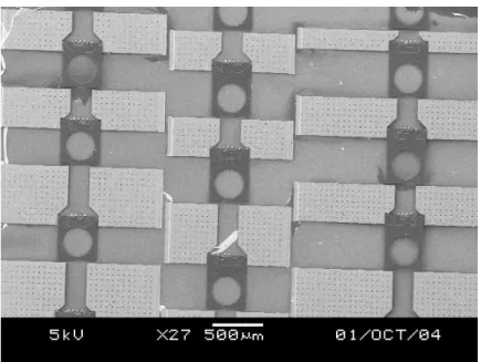
(64) Figure 4-21: Hinge bar group in the not to be vertical device2. 4-2 Fresnel lens The SEM picture of a SU-8 Fresnel Lens is shown in Figure 4-22. This is a 5mm focal length lens. Figure 4-23 is a magnified picture of the rings of the lens in Figure 4-22.. Figure 4-22: SU-8 Fresnel lens 54.
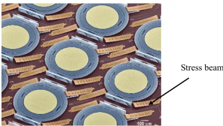
數據
![Figure 1-2: SEM micrograph of the monolithic optical-disk pickup head [3]. Figure 1-2 is a single-chip optical-disk pickup head developed by M](https://thumb-ap.123doks.com/thumbv2/9libinfo/8247120.171554/13.892.144.758.165.454/figure-micrograph-monolithic-optical-pickup-figure-optical-developed.webp)

+7


相關文件
Microphone and 600 ohm line conduits shall be mechanically and electrically connected to receptacle boxes and electrically grounded to the audio system ground point.. Lines in
structure for motion: automatic recovery of camera motion and scene structure from two or more images.. It is a self calibration technique and called automatic camera tracking
Although the standpoint of The Techniques of Samatha and Vipaśyana in Mah yāna Buddhism is different from the viewpoint of Hui-shih, its stress on the vajra prajñā is considered
substance) is matter that has distinct properties and a composition that does not vary from sample
The Secondary Education Curriculum Guide (SECG) is prepared by the Curriculum Development Council (CDC) to advise secondary schools on how to sustain the Learning to
Wang, Solving pseudomonotone variational inequalities and pseudocon- vex optimization problems using the projection neural network, IEEE Transactions on Neural Networks 17
We explicitly saw the dimensional reason for the occurrence of the magnetic catalysis on the basis of the scaling argument. However, the precise form of gap depends
Define instead the imaginary.. potential, magnetic field, lattice…) Dirac-BdG Hamiltonian:. with small, and matrix
