IEEE TRANSACTIONS ON CIRCUITS AND SYSTEMS FOR VIDEO TECHNOLOGY, VOL. 15, NO. 3, MARCH 2005 445
A Memory-Efficient Realization of Cyclic Convolution
and Its Application to Discrete Cosine Transform
Hun-Chen Chen, Jiun-In Guo, Tian-Sheuan Chang, and Chein-Wei Jen
Abstract—This paper presents a memory-efficient approach to realize the cyclic convolution and its application to the discrete cosine transform (DCT). We adopt the way of distributed arith-metic (DA) computation, exploit the symmetry property of DCT coefficients to merge the elements in the matrix of DCT kernel, separate the kernel to be two perfect cyclic forms, and partition the content of ROM into groups to facilitate an efficient realiza-tion of a one-dimensional (1-D) -point DCT kernel using ( -1)/2 adders or substractors, one small ROM module, a barrel shifter, and(( 1) 2) + 1 accumulators. The proposed memory-ef-ficient design technique is characterized by rearranging the con-tent of the ROM using the conventional DA approach into several groups such that all the elements in a group can be accessed si-multaneously in accumulating all the DCT outputs for increasing the ROM utilization. Considering an example using 16-bit coeffi-cients, the proposed design can save more than 57% of the delay-area product, as compare with the existing DA-based designs in the case of the 1-D seven-point DCT. Finally, a 1-D DCT chip was im-plemented to illustrate the efficiency associated with the proposed approach.
Index Terms—Cyclic convolution, discrete cosine transform (DCT), distributed arithmetic.
I. INTRODUCTION
D
UE to the high computational complexity and real-time processing requirements, the efficient hardware im-plementation of discrete cosine transform (DCT) is still a challenging problem, which plays a key function in image and signal processing, especially for the demanding multimedia and portable applications. To achieve efficient hardware re-alization, many researches have been done on realizing the multiplications needed in the DCT through ROM. One is the memory-based systolic array design [1] in which the proposed cyclic convolution-based architecture possesses the features of simple I/O behavior and removes the data redundancy in the DCT coefficients. The others are called distributed arithmetic (DA) based designs [2]–[11]. The DA technique is an efficient method for computing inner products by using ROM tables or adders, and accumulators [2]–[14]. It has been widely adopted in many DSP applications such as discrete Fourier transform (DFT), DCT, convolution, and digital filters. Therefore, there has been great interest in reducing the ROM size required in Manuscript received December 20, 2002; revised August 17, 2004. This paper was recommended by Associate Editor R. Chandramouli.H.-C. Chen, T.-S. Chang, and C.-W. Jen are with the Department of Elec-tronics Engineering and the Institute of ElecElec-tronics, National Chiao Tung University, Hsin-Chu 300, Taiwan, R.O.C. (e-mail: [email protected]. edu.tw; [email protected]; [email protected])
J.-I. Guo is with the Department of Computer Science and Information Engineering, National Chung Cheng University, Chia Yi 621, Taiwan, R.O.C. (e-mail: [email protected]).
Digital Object Identifier 10.1109/TCSVT.2004.842608
the implementation of the DA-based architectures [2], [7]–[9], [11]. Most of the DA-based designs exploit some memory reduction techniques such as the partial sum techniques and the offset binary coding (OBC) techniques [2], [8]. The other kind of DA-based design is realized by using adders and ac-cumulators. Chang [12] took advantage of the shared partial sum-of-products and sparse nonzero bits in the fixed input to reduce the number of computations. Guo [13], [14] exploited the feature of cyclic convolution to simplify the computation so that the multiplications and additions can be realized by using a small number of adders. However, their designs are still not efficient enough since they only exploit the constant property of the transform coefficients without considering further optimization in reducing hardware.In this paper, we appropriately combine the features of cyclic convolution and DA technique to propose a memory-efficient architecture in realizing the cyclic convolution and apply it to the one-dimen-sional (1-D) DCT. By exploiting the cyclic convolution, we find that different DCT outputs can be computed using the same coefficients and the same input data in a rotated order. If we directly realize the DCT using conventional DA technique [2], we find that ROM modules are used and only one word in a ROM module is accessed at a time in computing the DCT outputs. This reveals a message that the ROM utilization is not good enough. To increase the ROM utilization, we rear-range the contents of ROM in a different way. That is, we first group the candidates of DA inputs with rotated order as the same candidate and then arrange the ROM contents in such a manner that the partial products for accumulating different DCT outputs according to the candidate are grouped together and accessed simultaneously. The partial products arranged in a group should be rotated before accumulating. In this way, the ROM module will contain only few groups of contents and only one ROM module, instead of identical ROM modules, is needed to compute the 1-D -point DCT. Unfortunately, due to the rotated input data in the input-data matrix of DCT possess different signs, it is not easy to apply the proposed approach directly to DCT realization. Exploiting the symmetry property of DCT coefficients, we merge the elements in the matrix of DCT kernel and separate the matrix to two perfect cyclic forms. Then, these two smaller perfect cyclic convolution forms can be realized with the proposed design approach efficiently. This realization facilitates reducing the ROM size significantly. As compared with the existing DA-based designs, for an example of 1-D seven-point DCT with 16-bit coefficients, the proposed design can save more than 57% of the delay-area product. Moreover, a 1-D DCT chip was implemented to illustrate the efficiency associated with the proposed approach. This design approach can also be applied to other transforms like the DFT, 1051-8215/$20.00 © 2005 IEEE
Fig. 1. Proposed memory-efficient architecture and the associated ROM content arrangement in realizing the cyclic convolution example shown in (2).
the discrete Hartley transform (DHT) and the discrete sine transform (DST) used in many DSP applications.
The rest of this paper is organized as follows. In Section II, we illustrate the proposed memory-efficient realization of cyclic convolution and its advantages over the conventional DA-based approach. In Section III, we illustrate the proposed design for 1-D DCT including the algorithm derivation, architecture de-sign, and chip design. In Section IV, we show the performance evaluation of the proposed design with the existing DCT de-signs. Finally, we conclude this paper in Section V.
II. MEMORY-EFFICIENT REALIZATION OFCYCLICCONVOLUTION
A. Proposed Approach
Let us first consider a cyclic convolution example
(1)
Using the commutative property of convolution, we can rewrite (1) as follows:
(2)
where are input data, are
coeffi-cients, and are output data. Observing (2), we find that different outputs in vector can be computed using the same input data with rotated order and the same set of coefficients . According to the DA technique,
using the same set of coefficients implies that identical ROM modules are used to compute all the different outputs, and using the same input data samples with rotated order implies that we can arrange the partial products generated from the rotated combinations of the input data samples as a group and these partial products can be accessed simultaneously in accumulating all the outputs. Fig. 1 shows the proposed memory-efficient architecture for computing the vector . We use a group ROM to store all the shared ROM content that contains only 24 words instead of 64 words needed in the conventional DA-based architecture. Meanwhile, we need an additional barrier shifter and address decoder. However, this part of the overhead is minor compared with the savings we get in the ROM size, as we analyzed in the previous works [11]. B. Advantages of the Proposed Approach
In the following, we focus on evaluating the delay time and hardware cost of the inner-product circuits realized by the pro-posed design approach and the conventional DA approach, re-spectively. For a fair comparison, we adopt the Avanti 0.35- m CMOS data-path cell-library [15] in the performance evalua-tion in terms of the delay-area product shown in Fig. 2. We find that the delay-area product of the inner-product design realized by the proposed approach is much lower than that of the con-ventional DA design as increases, which illustrates that the proposed approach possesses better performance than the con-ventional DA-based approach does.
III. PROPOSEDMEMORYEFFICIENTDESIGN FOR1-D DCT A. Algorithm Derivation
If transform length is prime, we can write the 1-D -point
IEEE TRANSACTIONS ON CIRCUITS AND SYSTEMS FOR VIDEO TECHNOLOGY, VOL. 15, NO. 3, MARCH 2005 447
convolution form by exploiting the property of I/O data permu-tation as
(3) where denotes the result of “ modulo ” for short, is a primitive element, and the sequence is defined as (4) By using the symmetry property of cosine kernel as
(5) we can rewrite the in (3) as
(6) To describe the proposed algorithm in more detail, we can write the kernel in a design example of 1-D seven-point DCT in matrix form as
(7)
where denotes . However, the input data elements of the kernel possess different signs so that it is not easy to apply the
Fig. 2. Delay-area product of the designs using the proposed approach and the conventional DA approach with 16-bit data word length.
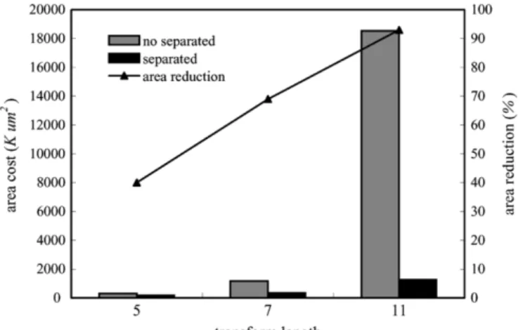
Fig. 3. Area reduction of the ROM cost whether or not applying the symmetry property of DCT coefficients.
proposed memory-efficient approach directly to DCT realiza-tion. According to the symmetry property of DCT coefficients as shown in (5), we can write (7) as
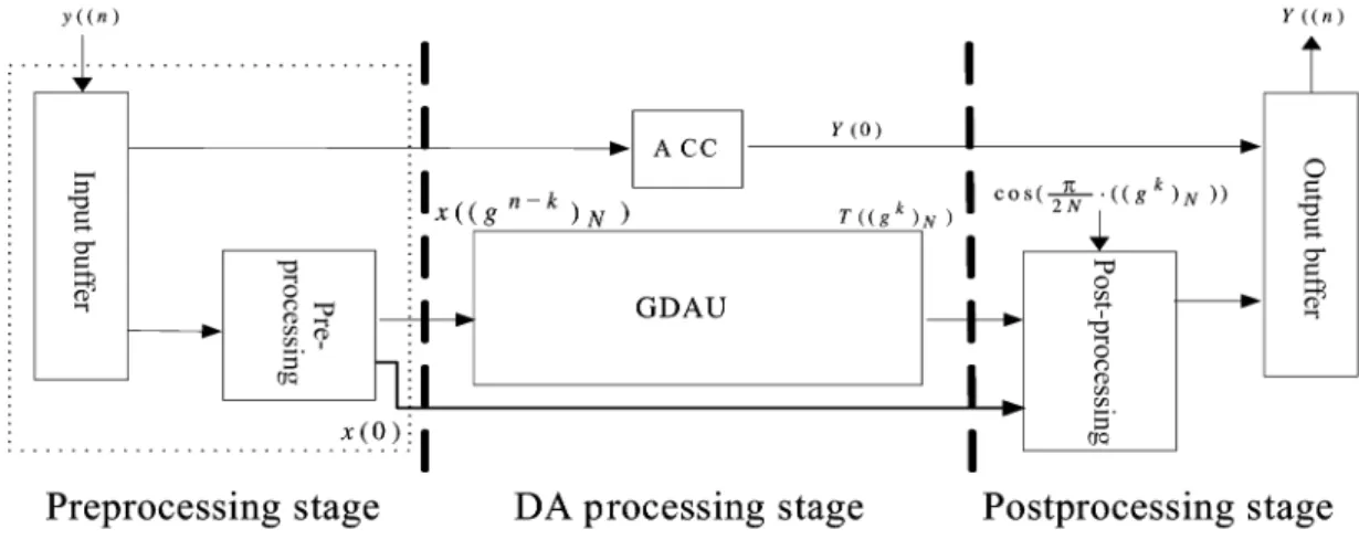
Fig. 4. Block diagram of the proposed pipeline architecture for computing the 1-DN-point DCT.
Fig. 5. Design of the preprocessing stage in the 1-D seven-point DCT.
and the data elements in the matrix of (8) can be merged as
(9)
To separate the even and odd outputs in (9), we can obtain two smaller, perfect cyclic convolution forms as follows:
IEEE TRANSACTIONS ON CIRCUITS AND SYSTEMS FOR VIDEO TECHNOLOGY, VOL. 15, NO. 3, MARCH 2005 449
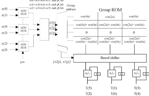
Fig. 6. Design of the DA processing stage that is used to compute the kernel ofT ((3 ) ) in the 1-D seven-point DCT.
(11) From (8) to (11), we find that exploiting the symmetry prop-erty of the DCT coefficient can help merging the input data el-ements in the DCT kernel and separating the kernel into two perfect cyclic forms, which facilitates the efficient realization of the DCT through the proposed design approach. Fig. 3 shows the area reduction of the ROM cost when applying the symmetry property of the DCT coefficients [shown in (10) and (11)] or not [shown in (7)]. We find that it is helpful in reducing the ROM size greatly when using the symmetry property of the DCT co-efficients.
For facilitating the proposed memory-efficient design ap-proach, we further formulate the specified in (6), as shown in (12) at the bottom of the page, where denotes the data word length of the variable , denotes the transform length, the variable denotes the th-bit group
TABLE I
SEEDVALUE, GROUPADDRESS,ANDROTATINGFACTORUSED IN THEDESIGN OFGROUPADDRESSDECODER OF1-D SEVEN-POINTDCT
address of the ROM access operations, and the preprocessed input sequence is defined as (13) and (14), shown at the bottom of the page. The value of is determined by
(15) (12) if if (13) if if (14)
TABLE II
PARTIALPRODUCTSDISTRIBUTION FORDIFFERENTDCT OUTPUTSUNDER THESAMEINPUTVALUE
TABLE III
EIGHT-WORDROM CONTENTSARRANGEDINTOGROUPS
B. Architecture Design
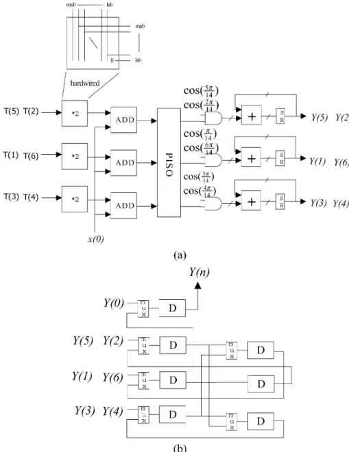
Fig. 4 shows the proposed pipeline architecture that realizes the 1-D N-point DCT. It consists of the preprocessing stage, the DA processing stage, and the post-processing stage. For the 1-D seven-point DCT design example, the input buffer and prepro-cessing in the preproprepro-cessing stage shown as Fig. 5 are designed by using the bidirectional shift registers and an accumulator, which is used to generate the data sequence from input sequence . The detail cycle information shows that the la-tency consumed by input data sampling and computation is 14 cycles. The DA processing stage shown as Fig. 6, named group distributed arithmetic unit (GDAU), is designed with the proposed memory-efficient approach to carry out the computa-tion of in the design example of 1-D seven-point DCT. Due to the same content of group ROM, only one group ROM in the GDAU is required to compute the outputs of the separated cyclic operations. In Fig. 6, the combined input vector
is first fed into an address decoder to de-termine which group it should belong to. The address decoder
will compute the seed value ,
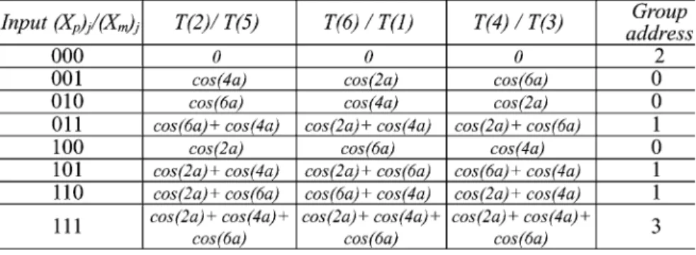
group address , and the rotating factor by decoding the input vector according to Table I. Table II shows the original partial product distributions for com-puting the outputs of DCT kernel under the same input value. From Table II, the rotation relationship between these partial products is also visible, and then the ROM content arrangement in the proposed design is shown in Table III. It is noted that we only need one small group ROM module of size
words for computing . As above, denotes the number of groups in the group ROM modules, which is de-pendent on the transform length . The post-processing stage shown in Fig. 7(a) is used to perform the post computation for GDAU outputs, including the operations of multiplying by two, added with and multiplied serially by the cosine coeffi-cients in formulation. Since the operation of multiplying by
two is performed by the manner of hardwiring, it has no hard-ware cost required. The output buffer shown in Fig. 7(b) in the post-processing stage is used to perform the operations of preloadable shifting for serially generating the results of DCT in order.
C. Chip Design
We have verified the proposed design for 1-D seven-point DCT in VERILOG modeling. According to the synthesis result with the Avanti 0.35- m cell library, this design consumes 7485 gates and possesses the maximum path delay of 12.1 ns. The working frequency of the chip is above 82.6 MHz. In other words, the chip can maintain the throughput rate of 18.1 M samples/s, i.e., MHz
cycles samples. Fig. 8 shows the layout view of the 1-D seven-point DCT chip fabricated using TSMC 0.35- m CMOS 1P4M process. The core size of proposed DCT
de-sign is equal to m .
IV. PERFORMANCEEVALUATION
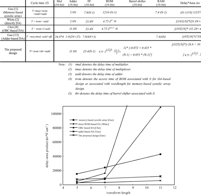
In this section, we will illustrate the performance evaluation of the design using the proposed design approach and some existing DCT designs. The existing DCT designs used in this evaluation include memory-based systolic array design [1], direct DA design [2], OBC DA design [8], and adder-based DA design [13]. For a fair comparison, we adopt the Avanti 0.35- m, 3.3-V CMOS cell library [15] in the performance evaluation in terms of the delay time and area cost. According to these two measures, we can evaluate these designs in terms of delay-area product with respect to different values of . Table IV shows the comparisons of these designs. The design in [1] is a ROM-based systolic array design. It needs about adders, -1 16-bit flip flop, and words of ROM if the ROM tables in the design are partitioned once. The silicon area of this design is equal to 1237 –1217 k m . The design in [2] is the conventional ROM-based DA design; it requires about 16-bit adders and 16-bit flip flops used for PISO and words of ROM. The silicon area of this design is equal to k m . The design in [8] is the modified ROM-based DA design using the reduction technique of OBC, it requires about 2 16-bit adders, 16-bit flip flop, and words of ROM. The silicon area of this design
IEEE TRANSACTIONS ON CIRCUITS AND SYSTEMS FOR VIDEO TECHNOLOGY, VOL. 15, NO. 3, MARCH 2005 451
Fig. 7. Design of the post-processing stage in the 1-D seven-point DCT, including (a) the post processing and (b) the output buffer.
Fig. 8. Layout view of the 1-D seven-point DCT chip.
[13] is the adder-based DA design; it requires about four 16-bit multipliers, , 16-bit adders, , 16-bit flip flops, and 4 words of RAM. The silicon area of this design is equal to K m . Fig. 9 shows the delay-area product of the proposed design and the existing designs [1], [2], [8], [13] in realizing the 1-D DCT with various values of . As shown in Fig. 9, in the case of 16-bit data word length, the delay-area product of the proposed design is much smaller than the ROM-based systolic array DCT design [1] and the other DA-based designs [2], [8], [13].
As for realizing the long-length DCT, with the issue of cyclic convolution partitioning, we suggest to partition the logn-length cyclic convolution to the short ones with Agarwal–Cooley al-gorithm [16] such that the logn-length DCT still consists of the short cyclic-convolution blocks. Thus, the proposed GDA de-sign can be extended to realize each of the shortened cyclic con-volution blocks for logn-length DCT to achieve low hardware cost and better delay-area product.
TABLE IV
COMPARISON OF THE PROPOSED DESIGN AND THEEXISTINGDCT DESIGNS [1], [2], [8], [13] INREALIZING THE1-D N-POINTDCTINTERMS OFDELAY ANDSILICONAREA
Fig. 9. Delay-area product of the proposed design and the existing DCT designs [1], [2], [8], [13] in realizing the 1-D DCT.
V. CONCLUSION
This paper presents a memory-efficient design for realizing the cyclic convolution and its application to the DCT. We com-bine the advantages of DA computation as well as the cyclic con-volution, and exploit the symmetry property of DCT coefficients to facilitate a memory-efficient realization of 1-D -point DCT kernel using adders or substractors, one small ROM module, a barrel shifter, and accumulators. To increase the ROM utilization, we rearrange the content of ROM into several groups in which all the elements in a group will be accessed simultaneously in computing all the DCT outputs. A 1-D seven-point DCT chip was designed and implemented to illustrate the efficiency associated with the proposed approach. Compared with the existing designs, the proposed design can
reduce more than 57% of the delay-area product. In summary, the proposed design approach can be easily applied in the trans-form problems trans-formulated into cyclic convolution.
REFERENCES
[1] J. I. Guo, C. M. Liu, and C. W. Jen, “The efficient memory-based VLSI array designs for DFT and DCT,” IEEE Trans. Circuits Syst. II., Exp.
Briefs, vol. 39, no. 10, pp. 723–733, Oct. 1992.
[2] S. A. White, “Applications of distributed arithmetic to digital sequence processing: A tutorial review,” IEEE Trans. Acoust. Speech Signal.
Process., vol. 6, no. 1, pp. 4–19, Jan. 1989.
[3] W. P. Burleson and L. L. Scharf, “A VLSI design methodology for dis-tributed arithmetic,” J. VLSI Signal Process., vol. 2, pp. 235–252, 1991. [4] Y. H. Chan and W. C. Siu, “On the realization of discrete cosine trans-form using the distributed arithmetic,” IEEE Trans. Circuits Syst. I., Reg.
IEEE TRANSACTIONS ON CIRCUITS AND SYSTEMS FOR VIDEO TECHNOLOGY, VOL. 15, NO. 3, MARCH 2005 453
[5] S. Wolter, A. Scubert, H. Matz, and R. Laur, “On the comparison between architectures for the implementation of distributed arithmetic,” in Proc.
IEEE Int. Symp. Circuits and Systems, vol. 3, May 1993, pp. 1829–1832.
[6] A. Madisetti and A. N. Wilson, “A 100 MHz 2-D8 3 8 DCT/IDCT processor for HDTV applications,” IEEE Trans. Circuits Syst. Video
Technol., vol. 5, no. 2, pp. 158–164, Apr. 1995.
[7] K. Nourji and N. Demassieux, “Optimal VLSI architecture for dis-tributed arithmetic-based algorithm,” in Proc. IEEE Int. Conf. Acoustics,
Speech, and Signal Processing, vol. 2, Apr. 1994, pp. 509–512.
[8] J. P. Choi, S. C. Shin, and J. G. Chung, “Efficient ROM size reduction for distributed arithmetic,” in Proc. IEEE Int. Symp. Circuits and Systems, May 2000, pp. II61–II64.
[9] M. Sheu, J. Lee, J. Wang, A. Suen, and L. Liu, “A high throughput-rate architecture for8 3 8 2-D DCT,” in Proc. IEEE Int. Symp. Circuits and
Systems, vol. 3, May 1993, pp. 1587–1590.
[10] W. K. Dae et al., “A compatible DCT/IDCT architecture using hard-wired distributed arithmetic,” in Proc. IEEE Int. Symp. Circuits and
Sys-tems, May 2001, pp. II457–II460.
[11] H. C. Chen, J. I. Guo, and C. W. Jen, “A new group distributed arithmetic design for the one dimensional discrete Fourier transform,” in Proc. IEEE Int. Symp. Circuits and Systems, May 2002, pp. I-421–I-424.
[12] T. S. Chang, C. Chen, and C. W. Jen, “New distributed arithmetic algo-rithm and its application to IDCT,” Proc. Inst. Elect. Eng., vol. 146, no. 4, pp. 159–163, Aug. 1999.
[13] J. I. Guo, “Efficient parallel adder based design for one dimensional discrete cosine transform,” Proc. Inst. Elect. Eng., vol. 147, no. 5, pp. 276–282, Oct. 2000.
[14] , “An efficient design for one dimensional discrete Hartley trans-form using parallel additions,” IEEE Trans. Signal Process., vol. 48, no. 10, pp. 2806–2813, Oct. 2000.
[15] AVANT!: 0.35 Micron 3.3-Volt High Performance Standard Cell Library, Avant! Corporation, 1996.
[16] R. C. Agarwal and J. W. Cooley, “New algorithms for digital convolu-tion,” IEEE Trans. Acoust., Speech, Signal Process., vol. ASSP-25, no. 5, pp. 392–410, Oct. 1977.