一維暨二維氧化鋅奈米光電特性及結構研究
134
0
0
全文
(2) 一維暨二維氧化鋅奈米光電特性及結構研究 Optoelectronic Characteristics and Structure Development of One- and Two-Dimensional Zinc Oxide Materials. 學生: 林晉慶. Student: Chin-Ching Lin. 指導教授: 陳三元. Advisor: Prof. Dr. San-Yuan Chen. 國立交通大學 材料科學與工程學系 博士論文 A Dissertation Submitted to Department of Materials Science and Engineering College of Engineering National Chiao Tung University In Partial Fulfillment of the Requirements for the Degree of Doctor of Philosophy in Materials Science and Engineering June 2006 Hsinchu, Taiwan, Repubile of China. 中華民國九十五年六月.
(3) Contents. Acknowledgments .....................................................................................3 Abstract......................................................................................................4 1 Introduction.........................................................................................6 1.1 Zinc oxide materials.......................................................................................6 1.2 Physical characteristics of ZnO materials......................................................8 1.2.1 Crystal and electronic band structures..................................................8 1.2.2 Electrical behaviors ............................................................................13 1.2.3 Luminescent properties ......................................................................17 1.2.4 Defects in ZnO ...................................................................................21 1.3 Doped ZnO materials...................................................................................23 1.3.1 N-type doping ....................................................................................23 1.3.2 P-type doping.....................................................................................24 1.4 Nanoscience and nanostructures in ZnO materials......................................26. 2. Theory and Experiment ...................................................................31 2.1. Theory..........................................................................................................31 2.1.1 Theoretical concepts of nanomaterials ...............................................31 2.1.2 Theoretical concepts of photoluminescence.......................................33 2.2 Material fabrication......................................................................................36 2.2.1 ZnO thin films formation ...................................................................36 2.2.2 Ions implantation in ZnO films ..........................................................37 2.2.3 Soft chemical growth and treatment on ZnO nanorods......................38 2.2.4 Fabrication of one-dimensional nanotube composite device .............38 2.3 Characterization of ZnO materials and electrical transport .........................40. 3. Defects engineering on zinc oxide thin films ..................................42 3.1 Introduction..................................................................................................42 3.2 Defects transition in high-orientated ZnO thin films...................................42 3.3 Point defects controlled by buffer layers in ZnO thin films system ............51 3.4 Summary......................................................................................................58 1.
(4) 4. Doped ZnO thin films by ion implantation ....................................59 4.1 Introduction..................................................................................................59 4.2 Phosphorous-implanted in ZnO thin films...................................................59 4.3 Characterization of p-type ZnO films..........................................................64 4.4 Summary......................................................................................................69. 5. Physical characteristics of ZnO nanorods via soft chemical process................................................................................................72 5.1 Introduction..................................................................................................72 5.2 ZnO nanorods array on organic substrate ....................................................72 5.3 Post-annealing effects on ZnO nanorods .....................................................79 5.4 Summary......................................................................................................85. 6. Plasma treatment on ZnO nanorods...............................................87 6.1 Introduction..................................................................................................87 6.2 High conductivity ZnO nanorods in hydrogen-plasma................................87 6.3 Rectifying behavior of ZnO nanorods by ammonia-plasma........................94 6.4 Summary....................................................................................................100. 7. One dimensional ZnO and carbon nanotube (CNT) composite.102 7.1 7.2 7.3 7.4 7.5. 8. Introduction................................................................................................102 Synthesis and characterization of ZnO-SWNT composite ........................103 Electrical transport in individual core-shell nanotube ...............................108 Ultraviolet photoresponse of single ZnO nanorod.....................................110 Summary....................................................................................................113. Conclusions......................................................................................114. References ..............................................................................................118 Curriculum Vitae ..................................................................................127 Publication list.......................................................................................128. 2.
(5) Acknowledgments First of all, I am deeply appreciative to my supervisor Prof. Dr. San-Yuan Chen for his all-out supports, useful discussions and kindness advices during my study period. Prof. Dr. San-Yuan Chen is not only a benevolent advisor but also a very erudite philosopher. I have benefited much from his philosophy of life. I also sincerely thank Dr. Syh-Yuh Cheng of the Industrial Technology Research Institution for his fruitful discussions and warmhearted help in my thesis work. Moreover, I am grateful to Prof. Dr. Klaus von Klitzing and my co-advisor Dr. Siegmar Roth for giving me an opportunity to visit their impressive department and enthusiastic laboratory during the period when I studied at Max-Planck Institut für Festkoerperforschung in Stuttgart of Germany. My works have largely been a collaborative effort. Therefore, I would like to thank my colleagues: Mr. Kun-Ho Liu, Mrs. Hung-Pei Chen, Mr. Pai-Chia Kuo, Miss Shu-Ping Lee, Mr. Hung-Chou Liao and Mr. Chi-Sheng Hsiao of the National Chiao Tung University in Taiwan and Dr. Miroslav Haluska, Prof. Dr. Viera Skakalova, Dr. Yun Sung Woo, Dr. Ursula Dettlaff, Dr. Martti Kaempgen, Dr. Jannik Meyer, Dr. Dirk Obergfell, Dr. Michael Schmid, Dr. Mitauharu Konuma, Dr. Michael Lebert, Prof. Dr. Po-Wen Chiu, Mr. Chen-Wei Liang, Mr. Jiangping Wang, Mr. Serhat Sahakalkan, Mr. Viktor Siegle, Mr. Bjoern Hornbostel, Mr. Alberto ansaldo, Mr. Thomas Reindl, Miss Franziska Koch and Mr. Jiri Cech of Max-Planck Institut für Festkoerperforschung in Stuttgart for supplying the valuable suggestions and sharing their time with me. Finally, I want to thank my family and friends for their selfless supports and encouragement during my study period.. Chin-Ching Lin, Taiwan, 10, 05, 2006 3.
(6) Abstract Zinc oxide (ZnO) has unique physical properties that make it a most promising material for optoelectronic device. The main reasons are a direct band gap of 3.3 eV and a large exciton binding energy (60 meV), which permits exciton recombination even above room temperature. Owing to its distinctive characteristics the research trend on ZnO has continued for many decades. The former studies are focused on the basic physical properties of three- and two-dimensional ZnO materials, such as lattice parameter, vibrational properties, and optical studies. As improving the technology of materials growth, scientists have more opportunities to produce high-quality ZnO materials and then can do deeply research in it. In this nearly decade, the main obstacle to the development of ZnO has been the lack of reproducible and low-resistivity p-type ZnO. For the moment, many groups have attacked this problem and several have been successful to solve some problems of them [64-67]. Moreover, theoreticians have also been active in this area, and have predicted the electrical activities of various dopants and native defects [68-70]. In addition to ZnO thin films, significant interest has emerged in the synthesis of nanoscale ZnO materials, in recent years. It is due to the one-dimensional ZnO nanostructures provide an attractive candidate system for fundamental quantization and low-dimensional transport studies for chemical sensing and biomedical applications. This thesis outlines the process of fabricating p-type ZnO thin films and one-dimensional ZnO nanostructures, as well as the study of their physical properties. In chapter 1 we will present an introductory overview to ZnO materials. It is devoted, respectively, fundamental, doping, and defects properties in ZnO. Chapter 2 will discuss the fabrication of one- and two-dimensional ZnO materials and basic 4.
(7) theoretical concepts of nanoscience. This chapter also includes how we developed high-quality ZnO films and nanorods and measured their excellent physical properties. The individual nanorod measurement setup for electrical transport is also shown in this chapter. Chapter 3 discusses the defects engineering on ZnO thin films. The transitions of native defects in ZnO are inspected by photoluminescence (PL) spectroscopy, in this study. Different buffer-layers could change the concentration of native defects and improve the physical properties of ZnO. We will, therefore, discuss the relationship between the predominant defects and PL emissions in the ZnO films. In chapter 4, we will present the results for the electrical and optical properties of group-V elements doping in ZnO films. Reproducible p-type ZnO films with high carrier concentration (7.3 × 1017 cm-3) are fabricated by nitrogen-implanted on nitride layer and then annealed at 850 oC in N2 ambient. To date, the most popular method to grow ZnO nanorods is vapor-solid process. However, this method is usually operated under high temperature and it has also locked the size of the sample due to the size of the furnace. In chapter 5, we will show a convenient method to produce large scale ZnO nanorods on organic and inorganic substrates. The growth mechanism and thermal annealed effect of ZnO nanorods will be investigated by high-resolution transmission electron microscopy. The plasma treatments are used to improve the luminescent and electrical properties in ZnO nanorods. The high conductivity n-type and rectifying behavior p-type ZnO nanorods are revealed in chapter 6. The electrical transport of individual ZnO nanorods and single-walled carbon nanotubes composite will be discussed in chapter 7.. 5.
(8) Chapter 1. Introduction 1.1. Zinc oxide materials. Nowadays, ZnO is attracting attention for its application to ultraviolet (UV) light-emitters, transparent high power electronics, surface acoustic wave devices, piezoelectric transducers, gas-sensing and solar cells. Some optoelectronic applications of ZnO have advantages over GaN, another wide-gap semiconductor (Eg ~3.4 eV at 300 K) and widely used for production of light-emitting devices, because of its availability in bulk, single-crystal form and its larger exciton binding energy (60 meV at 300K) [1-15]. As a wide bandgap semiconductor, ZnO is a candidate host for solid state blue to UV optoelectronics, including laser development. This has important applications in high density data storage systems, solid-state lighting, secure communications and bio-detection [16]. Transparency to visible light provides opportunities to develop transparent electronics, UV optoelectronics, and integrated sensors, all from the same material system. ZnO is a direct bandgap semiconductor with Eg~3.2 eV. The bandgap of ZnO can be tuned via divalent substitution on the cation site. It is well-known that ZnO is not really a newly discovered material. Interest in this material at the time of this writing is again at a high point. In terms of its characterization, reports go back to 1935 or even earlier. Studies of ZnO properties presume that ZnO samples were available. Growth methods not much different from. 6.
(9) what is employed lately have been explored, among which are chemical-vapor transport, vapor-phase growth, hydrothermal, high-quality platelets. ZnO has recently found other niche applications as well, such as fabrication of transparent thin-film transistors, where the protective covering preventing light exposure is eliminated since ZnO-based transistors are insensitive to visible light. Today scientists can use heavy substitutional doping method to increase the carrier concentrations up to 2x1021 cm−3. By controlling the doping level electrical properties can be changed from insulator through n-type semiconductor to metal while keeping optical transparency that makes it useful for transparent electrodes in flat-panel displays and field effect transistor. However, an important problem should be overcome before ZnO transforms into a potential optoelectronics devices in the world: the fabrication of p-type-conductivity ZnO materials. Notwithstanding all the progress that has been made and the reports of p-type conductivity in ZnO films using various growth methods and various group-V dopant elements (N, P, and As), a reliable and reproducible high quality p-type conductivity has not yet been achieved for ZnO. Therefore, it remains to be the major topic in ZnO research today, and congruently most of the research efforts are directed just to solving this problem. Many results are just heralds of what can be expected of ZnO in an effort to position it for future device applications. As in the early developments of GaN predating the demonstration of p-type conductivity, metal-insulator-semiconductor device structures not requiring p-type ZnO have been introduced but lack the high efficiency.. 7.
(10) 1.2. Physical characteristics of ZnO materials. 1.2.1 Crystal and electronic band structures. (i) Crystal structure. Most of the group II-VI binary compound semiconductors crystallize in either cubic zinc-blende or hexagonal wurtzite structure where each anion is surrounded by four cations at the corners of a tetrahedron, and vice versa. This tetrahedral coordination is typical of sp3 covalent bonding, but these materials also have a substantial ionic character. ZnO is an II-VI compound semiconductor whose ionicity resides at the borderline between covalent and ionic semiconductor. The crystal structures shared by ZnO are wurtzite, zinc blende, and rocksalt. At ambient conditions, the thermodynamically stable phase is wurtzite, as schematically shown in Figure 1.1a. The zinc-blende ZnO structure can be stabilized only by growth on cubic substrates, and the rocksalt structure may be obtained at relatively high pressures. The wurtzite structure has a hexagonal unit cell with two lattice parameters, a and c, in the ratio of c/a=1.633 and belongs to the space group of P63mc. The structure is composed of two interpenetrating hexagonal-close-packed sublattices, each of which consists of one type of atom displaced with respect to each other along the threefold c-axis by the amount of u =3/8=0.375 (in an ideal wurtzite structure) in fractional coordinates. Each sublattice includes four atoms per unit cell and every atom of one kind (group-II atom) is surrounded by four atoms of the other kind (group VI), or vice versa, which are coordinated at the edges of a tetrahedron [17]. In a real ZnO crystal,. 8.
(11) the wurtzite structure deviates from the ideal arrangement, by changing the c/a ratio or the u value. It should be pointed out that a strong correlation exists between the c/a ratio and the u parameter in that when the c/a ratio decreases, the u parameter increases in such a way that those four tetrahedral distances remain nearly constant through a distortion of tetrahedral angles due to long-range polar interactions. Since the c/a ratio also correlates with the difference of the electron negativities of the two constituents, components with the greatest differences show the largest departure from the ideal c/a ratio. The convention is that the [0001] axis points from the face of the O plane to the Zn plane and is the positive z direction. In other words, when the bonds along the c direction are from cation (Zn) to anion (O), the polarity is referred to as Zn polarity. By the same argument, when the bonds along the c direction are from anion (O) to cation (Zn), the polarity is referred to as O polarity. Many properties of the material depend also on its polarity, for example, growth, etching, defect generation and plasticity, spontaneous polarization, and piezoelectricity. In wurtzite ZnO, besides the primary polar plane (0001) and associated direction <0001>, which are the most commonly used surface and direction for growth, many other secondary planes and directions exist in the crystal structure.. (ii) Electronic band structures. The band structure of a given semiconductor is pivotal in determining its potential utility. Consequently, an accurate knowledge of the band structure is critical if the semiconductor in question is to be incorporated in the family of materials considered for device applications. Several theoretical approaches of varying degrees of complexity have been employed to calculate the band structure of ZnO for its wurzite, 9.
(12) zinc-blende, and rocksalt. Figure 1.1b shows the calculated band structure and the total density of states of ZnO for wurzite phase. Besides, a number of experimental data have been published regarding the band structure of the electronic states of wurtzite ZnO. X-ray or UV reflection/absorption or emission techniques have conventionally been used to measure the electronic core levels in solids. These methods basically measure the energy difference by inducing transitions between electronic levels. For example, transitions from the upper valence band states to the upper conduction band states, and from the lower valence-band states, or by exciting collective modes,such as, the upper core states to the lower edge of the conduction band and to excitations of plasmons. After the theoretical work on band-structure calculation of ZnO proposed by Rössler using Green’s function in 1969, there have been several experimental works [18-19] performed on the wurtzite ZnO which proved Rössler’s predicted bulk electronic structure to be far from satisfactory. Langer and Vesely [20] have reported experimental data related to the energy levels of core electrons in ZnO using x-ray-induced photoemission spectroscopy. They have drawn two conclusions from their studies: (a) the location of the Zn 3d level in ZnO has been unambiguously determined and (b) the discrepancy between the measured values and the theoretically determined energy values was angular momentum dependent. Powell et al. [18] have carried out UV photoemission measurements on hexagonal ZnO cleaved in vacuum. Those authors have placed the Zn 3d core level at about 7.5 eV below the valence-band maximum, which is 3 eV lower than the value predicted by Rössler’s band calculation. In the following years, LDA and tight binding methods were employed [21,22] by considering the Zn 3d states as core levels to ease calculations. Satisfactory agreement with qualitative valence-band dispersions was achieved with this assumption. However, quantitative disagreements remained and the location of the Zn 3d states could not be predicted. 10.
(13) Figure 1.1: (a) Crystal structure, and (b) Band structure for wurtize type in the ZnO [33].. Recently, Girard et al. [23] have studied the electronic structure of the ZnO (0001) surface by angle-resolved photoelectron spectroscopy. They recorded both normal and off normal emission spectra, which give valuable information about bulk and surface states as well as the Zn 3d states. In these measurements, the binding energies were referred to the Fermi level and the intensities were normalized to the photon flux. Among all the spectra displayed, seven features were seen, labeled from A to G. The dispersions of the four valence bands observed in the (0001) direction were compared with theory based on LDA calculations, which consider the Zn 3d electrons as part of the valence band, [24] and good agreement was realized. It should also be noted that the Zn 3d states were observed to separate into two groups of four and six bands, which show dispersion with k, which is in agreement with theoretical results, but the. 11.
(14) location of these states were not accurately predicted. The polar (0001)-Zn and (000-1)-O surfaces and the nonpolar (10-10) surface (m plane) have also been the object of experimental and theoretical investigations. Of these surfaces, the nonpolar (10-10) surface is of particular interest from the viewpoint of surface chemistry, because the surface is terminated with the same number of O and Zn atoms. The low-energy electron-diffraction (LEED) studies have revealed that the surface undergoes relaxation, which is characterized by downward shift of both surface Zn and O atoms, with a greater shift for the Zn atom than the O atom, resulting in the Zn–O bond rotation by 6.2° or 11.5° [25] with respect to the ideal surface plane. Such a surface relaxation should influence the energetic position as well as the dispersion width of the surface dangling bond bands of the occupied O 2p and unoccupied Zn 4s states. Besides, several theoretical studies have indicated that, upon relaxation, the O 2p dangling-bond state is stabilized while the Zn 4s dangling-bond state shifts up in energy. [26] The theoretically determined position of these dangling-bond bands, especially the occupied O 2p dangling-bond band, relative to the bulk bands projected onto the (10-10) surface varies depending on the method employed in the calculations. The theoretical calculation of the band structure of ZnO mostly involve the LDA, [24,27,28]which is very demanding because of the cationic d electrons. If the d electrons are treated as core electrons, the calculated lattice constant underestimates the experimental values by as much as 18% for wurtzite ZnO, while inclusion of the d electrons in the valence band yields very accurate lattice constants. However, even if the d electrons are properly taken into account, the results of standard LDA calculations show distinct shortcomings, such as strongly underestimated band gap and overestimated occupied cationic d bands, which roughly reside 3 eV high in energy as compared to experiment. In addition, their interactions with the anion p 12.
(15) valence bands are artificially enlarged, resulting in overestimated dispersion and bandwidth of the latter and shifting them unphysically close to the conduction bands. Zakharov et al. [29] have recently reported plane-wave GW method for a number of II-VI compounds. They simply treated the d electrons as core electrons and deliberately carried out their GW calculation at the experimental lattice constants. They obtained very good results for the anion p valence bands and for the band-gap energies but no assertion concerning the d-band positions could be made. Recently, Vogel et al. [30] suggested an alternative approach to treat the II-VI semiconductor compounds, which approximately incorporates dominant self-interaction corrections. It has been shown that self-interaction corrections to LDA can be very important for a quantitative description of a system with strongly localized states such as 3d electrons. The electronic band structure of the other phases of ZnO has also been studied by a number of researchers [30-32]. When wurtzite ZnO is compressed, it has been observed that the peak at the top of the upper valence band is slightly reduced in height and shifted down in energy, the O 2s and Zn 3d-derived peaks are slightly broadened and shifted up in energy, and a splitting appears in the Zn 3d states.. 1.2.2 Electrical behaviors. As a direct and large-band-gap material, ZnO is attracting a lot of attention for a variety of electronic and optoelectronic applications. Advantages associated with a large band gap include higher breakdown voltages, ability to sustain large electric fields, lower noise generation, and high temperature and high power operation. The electron transport in semiconductors can be considered for low and high electric fields. (a) At sufficiently low electric fields, the energy gained by the electrons from the applied electric field is small compared to the thermal energy of electrons, and 13.
(16) therefore, the energy distribution of electrons is unaffected by such a low electric field. Since the scattering rates determining the electron mobility depend on the electron distribution function, electron mobility remains independent of the applied electric field, and Ohm’s law is obeyed. (b) When the electric field is increased to a point where the energy gained by electrons from the external field is no longer negligible compared to the thermal energy of the electron, the electron distribution function changes significantly from its equilibrium value. These electrons become hot electrons characterized by an electron temperature larger than the lattice temperature. Furthermore, as the dimensions of the device are decreased to submicron range, transient transport occurs when there is minimal or no energy loss to the lattice during a short and critical period of time, such as during transport under the gate of a field-effect transistor or through the base of a bipolar transistor. The transient transport is characterized by the onset of ballistic or velocity overshoot phenomenon. Since the electron drift velocity is higher than its steady-state value, one can design a device operating at frequencies exceeding those expected from linear scaling of dimensions. Hall effect is the most widely used technique to measure the transport properties and assess the quality of epitaxial layers. For semiconductor materials, it yields the carrier concentration, its type, and carrier mobility. More specifically, experimental data on Hall measurements over a wide temperature range, as 4.2–300 K, provide quantitative information on impurities, imperfections, uniformity, scattering mechanisms, etc. The Hall coefficient and resistivity (ρ) are experimentally determined and then related to the electrical parameters through (for n-type conduction) RH=rH/ne and µH =RH/ρ, where n is the free-electron concentration, e is the unit electronic charge, µH is the Hall mobility, and rH is the Hall scattering factor which is dependent on the particular scattering mechanism. The drift mobility is the 14.
(17) average velocity per unit electric field in the limit of zero electric field and is related to the Hall mobility through the Hall scattering factor by µH =rHµ. As noted above, the Hall scattering factor depends on the details of the scattering mechanism, which limits the drift velocity. As the carriers travel through a semiconductor, they encounter various scattering mechanisms that govern the carrier mobility in the electronic system. The parameter for characterizing the various scattering mechanisms is the relaxation timeτ, which determines the rate of change in electron momentum as it moves in the semiconductor crystal. Experimental investigation of the temperature-dependent carrier mobility and concentration can be used to determine the fundamental material parameters and understand the carrier scattering mechanisms along with an accurate comparison with theory. The transport properties reported in the literature are mostly based on Hall-effect measurements, assuming the Hall scattering factor to be unity. Using Monte Carlo simulations, Albrecht et al. [34,35] predicted the room-temperature electron mobility of ZnO as 300 cm2/Vs. Nominally undoped ZnO with a wurtzite structure naturally becomes an n-type semiconductor due to the presence of intrinsic or extrinsic defects, which were generally attributed to native defects, such as OZn, Zni, and VO.. Ohmic and Schottky contacts on ZnO. An Ohmic contact can be defined as having a linear and symmetric current-voltage relationship for both positive and negative voltages and is so important for carrying electrical current into and out of the semiconductor, ideally with no parasitic resistance. The major loss of device performance is often caused by high-resistance metal-semiconductor Ohmic contacts through thermal stress and or contact failure 15.
(18) [36]. Thus, in order to attain high-performance ZnO-based optical and electrical devices, it is essential to achieve Ohmic contacts that have both low resistance and are thermally stable and reliable. This can be achieved either by performing surface preparation to reduce the metal-semiconductor barrier height which would allow to increase carrier tunneling probability or by increasing the effective carrier concentration of the surface perhaps taking advantage of oxygen loss [37,38]. In ZnO, Specific contact resistances of 3x10⁻⁴ Ωcm2 were reported for Pt-Ga contacts on n-ZnO epitaxial layers [39], 2x10⁻⁴ Ωcm2 for Ti/Au on Al-doped epitaxial layers [40], 0.7 Ωcm2 for non-alloyed In on laser-processed n-ZnO substrates [41], 2.5x10⁻⁵ Ωcm2 for non-alloyed Al on epitaxial n-type ZnO [42], 7.3x10⁻³ to 4.3x10⁻⁵ Ωcm2 for Ti/Au on plasma exposed, Al-doped n-type epitaxial ZnO [43] and 9 x10⁻⁷ Ωcm2 for Ti/Al on n+ epitaxial ZnO [44]. The chemical reactions between the metal and the semiconductor, the surface states, the contaminants, the defects in the surface layer, and the diffusion of the metal into the semiconductor are well-known problems in the formation of Schottky contacts. To create Schottky barrier with undoped ZnO, a high work function can be applied to the surface of a ZnO crystal. Many publications reveal that Au has some serious problems at high temperatures, [45,46] but it has widely been applied to ZnO to form Schottky barriers [45-47]. Au and Ag Schottky contacts on (0001) Zn surface of undoped n-ZnO samples have been investigated by Polyakov et al., [46] comparing their barrier heights and thermal stabilities. Schottky barrier heights of 0.65–0.69 eV and diode ideality factors of 1.6–1.8 have been obtained by capacitance-voltage and current-voltage measurements, respectively. The ideality factor had a value close to 2 for almost all the samples studied due to an increase of the tunneling current through the junction. Some authors have reported good electrical performance of the Schottky diodes after etching in concentrated nitric acid [48]. However, it should be noted that 16.
(19) in the majority of papers the ideality factors of the ZnO Schottky diodes are considerably higher than unity which has been explained by the prevalence of tunneling, the impact of interface states or the influence of deep recombination centers.. 1.2.3 Luminescent properties. (i) Basic concept of excitons. The absorption of a photon by an interband transition in a semiconductor or insulator creates an electron in the conduction band and a hole in the valence band. The oppositely charged particles are created at the same point in space and can attract each other through their mutual Coulomb interaction. This attractive interaction increases the probability of the formation of an electron-hole pair, and therefore increases the optical transition rate. Moreover, if the right conditions are satisfied, a bound electron-hole pair can be formed.. This neutral bound pair is called an exciton. In the. simplest picture, the exciton may be conceived as a small hydrogenic system similar to a positronium atom with the electron and hole in a stable orbit around each other. Excitons are observed in many crystalline materials. There are two basic types of excitons, Wannier-Mott excitons (free excitons) and Frenkel excitons (tightly bound excitons). The free excitons are mainly observed in semiconductors, while the Frenkel excitons are found in insulator crystals and molecular crystals. Moreover, Wannier-Mott type excitons have a large radius that encompasses many atoms, and they are delocalized states that can move freely throughout the crystal; hence the alternative name of “free” excitons. In contrast, Frenkel excitons have a much smaller radius which is comparable to the size of the unit cell. This makes them localized 17.
(20) states which are tightly bound to specific atoms or molecule; hence their alternative name of “tightly bound” excitons. Tightly bound excitons are much less mobile than free excitons, and they have to move through the crystal by hopping from one atom site to another [49]. In a free exciton, the average separation of the electrons and holes is much greater than the atomic spacing, as shown in Figure 1.2(a). This is effectively the definition of a Wannier exciton, and it specifies more accurately what is meant by saying that the free exciton is a weakly bound electron-hole pair. Since the electron-hole separation is so large, it is a good approximation to average over the detailed structure of the atoms in between the electron and hole and considers the particles to be moving in a uniform dielectric material. The energies of the bound states can be determined by finding the eigenvalues of the Schroedinger equation for the relative motion, or alternatively by using approximation techniques such as the variational method. Bound excitons are localized on the atom site at which they are created, as shown in Figure 1.2(b). The excitons may therefore be considered as excited states of the individual atoms or molecules on which they are localized. They have very small radii and correspondingly large binding energies, with typical values ranging from about 0.1 eV to several eV. This means that Bound excitons are usually stable at room temperature. The excitons can propagate through the crystal by hopping from atom site to site in the same way that spin excitations propagate through crystals as magnon waves. The theoretical treatment of Bound excitons requires techniques more akin to atomic or molecular physics than solid state physics. The calculation of the exciton energies usually follows a tight binding approach, in order to emphasize the correspondence to the atomic or molecular states from which the excitons are derived. The calculation is further complicated by the fact that the coupling between the excitons and the crystal lattice is usually very strong. This leads to ‘self-trapping’ 18.
(21) effects, in which the exciton produces a local distortion of the lattice, which then causes further localization of the exciton wave functions.. Figure 1.2: Schematic diagram of (a) Wannier-Mott excitons and (b) Frenkel excitons.. (ii) Free and Bound excitons in ZnO. The wurtzite ZnO conduction band is mainly constructed from the s-like state having Γ7c symmetry, whereas the valence band is a p-like state, which is split into three bands due to the influence of crystal-field and spin-orbit interactions [50]. The near-band-gap intrinsic absorption and emission spectrum is therefore dominated by transition from these three valence bands. The related free-exciton transitions from the conduction band to these three valence bands or vice versa are usually denoted by the heavy hole, light hole, and crystal-field split band. Bound excitons are extrinsic transitions and are related to dopants or defects, which usually create discrete electronic states in the band gap, and therefore influence both optical absorption and emission processes. The electronic states of the bound. 19.
(22) excitons depend strongly on the semiconductor material, in particular, the band structure. From above statement, excitons could be bound to neutral or charged donors and acceptors. A basic assumption in the description of the bound exciton states for neutral donors and acceptors is a dominant coupling of the like particles in the bound-exciton states. These two classes of bound excitons are by far the most important cases for direct band-gap materials. In high-quality bulk ZnO substrates, the neutral shallow neutral-donor bound exciton (DBE) often dominates because of the presence of donors due to doped impurities and/or shallow donor-like defects. In samples containing acceptors, the acceptor-bound excitons (ABE) is observed. The recombination of bound excitons typically gives rise to sharp lines with a photon energy characteristic to each defect. Many sharp donor and acceptor bound-exciton lines were reported in a narrow energy range from 3.348 to 3.374 eV in ZnO. However, the chemical origin and binding energy of the most underlying donor and acceptor atoms remain unclear.. (iii) Two-electron satellites and Stimulated emission in ZnO. Another characteristic of the neutral-donor-boundexciton transition is the two-electron satellite transition in the spectral region of 3.32–3.34 eV. These transitions involve radiative recombination of an exciton bound to a neutral donor, leaving the donor in the excited state, thereby leading to a transition energy which is less than the DBE energy by an amount equal to the energy difference between the first excited and ground states of the donor. In the effective-mass approximation, the energy difference between the ground-state neutral donor-bound excitons and their excited states can be used to determine the donor binding energies [51] and catalog the different species present in the material. 20.
(23) Even though n- and p-type dopings have been reported in ZnO thin-films, [52] there is no demonstration of electrically pumped lasing in ZnO-based structures. However, optically pumped stimulated emission has been observed by many researchers from ZnO epitaxial layers grown by a variety of methods. Fabrication of low-dimensional structures such as quantum wells and dots has been the focus of semiconductor laser research to decrease the threshold for lasing. Efficient stimulated emission may be obtained from these quantum structures since the transfer integral at the band edge is larger than that of the bulk semiconductor. Excitonic emission may also be used to obtain efficient lasing, which may be realized for ZnO due to its larger exciton binding energy (60 meV) [53] compared to other wide band-gap semiconductors. Exciton-exciton scattering-induced stimulated emission is very important for the realization of low-threshold lasers since it occurs at a threshold lower than that for the electron-hole plasma (EHP) recombination. The demonstration of stimulated emission with excitonic origin paves the way for the realization of blue-violet laser diodes based on ZnO.. 1.2.4 Defects in ZnO. As in any semiconductor, point defects affect the electrical and optical properties of ZnO as well. Kohan et al. and Van de Walle [54,55] recently calculated formation energies and electronic structure of native point defects and hydrogen in ZnO by using the first-principles, plane-wave pseudopotential technique together with the supercell approach. It can be concluded that, depending on the partial pressure of Zn, the two most common defects in ZnO are likely to be oxygen and zinc vacancies. In particular, oxygen vacancies (VO) have lower formation energy than the zinc interstitials (Zni) and hence should be more abundant in Zn-rich conditions. In O-rich 21.
(24) conditions, zinc vacancies (VZn) should dominate. Figure 1.3 shows the various structure of native defects in ZnO crystal. As for the electronic structure of the main point defects in ZnO, the oxygen vacancy has been identified as a negative-U defect, since with increasing Fermi level a transition occurs from the +2 to the neutral state. Zinc vacancy is expected to have charge −2 in n-type ZnO where its formation is more favorable. The transition level between the −1 and −2 charge states of VZn occurs at 0.8 eV above the valence band. Thus, we may expect transitions from the conduction band or a shallow donor to the VZn acceptor at around 2.6 eV in n-type ZnO. Thus, the broad green luminescence commonly observed in n-type ZnO can be attributed to VZn [54]. The 2+ /0 level of the oxygen vacancy is predicted at about 2.7 eV above the valence band [55]. Since the positive charge state of VO is unstable in ZnO, an electron paramagnetic resonance signal associated with this defect is not expected to be observable, at least in thermodynamically stable conditions.. Figure 1.3: Structures of fully relaxed (a) Zno and , (b) OZn antisite, and (c) Zni point defects. (The dark balls indicate O atoms, whereas the gray balls are Zn atoms) [154]. Besides strong and rich exciton-related emissions in the photon energy range of 3.25–3.4 eV, PL spectrum of undoped high-quality ZnO usually contains a sharp peak at about 3.22 eV followed by at least two LO-phonon replicas. This emission has been. 22.
(25) attributed to the donor-acceptor pair (DAP) transitions involving a shallow donor and a shallow acceptor [56]. This conclusion is based mostly on a characteristic transformation of the DAP emission lines to similar, but shifted, emission lines arising from transitions from the conduction band to the same shallow acceptor with increasing temperature. The nature of the Green Luminescence, appearing at about 2.5 eV in undoped ZnO, may be related to a native point defect such as VO or VZn. A red luminescence band emerged at about 1.75 eV in the PL spectrum of undoped bulk ZnO. Doping ZnO with Li acceptor results in the yellow luminescence band with a peak at about 2.2 eV. In contrast to the Green Luminescence band, the yellow luminescence band decays very slowly after switching off the excitation source, and can be observed also in the thermal luminescence spectrum [14].. 1.3 Doped ZnO materials. ZnO has a strong potential for various short-wavelength optoelectronic device applications. In order to attain the potential offered by ZnO, both high-quality n- and p-type ZnO are indispensable. However, difficulty in bipolar carrier doping is a major obstacle as seen in other wide-band-gap semiconductors.. 1.3.1 N-type doping. ZnO with a wurtzite structure is naturally an n-type semiconductor because of a deviation from stoichiometry due to the presence of intrinsic defects such as O vacancies and Zn interstitials. Undoped ZnO shows intrinsic n-type conductivity. The first-principles study suggested that none of the native defects show high. 23.
(26) concentration shallow donor characteristics [54]. N-type doping of ZnO is relatively easy compared to p-type doping. Group-III elements Al, Ga, and In as substitutional elements for Zn and group-VII elements Cl and I as substitutional elements for O can be used as n-type dopants [57]. Doping with Al, Ga, and In has been attempted by many groups, resulting in high-quality, highly conductive n-type ZnO films [58-60].. 1.3.2 P-type doping. As mentioned repeatedly it is very difficult to obtain p-type doping in wide-band-gap semiconductors, such as GaN and ZnSe. The difficulties can arise from a variety of causes. Dopants may be compensated by low-energy native defects, such as Zni or VO. Low solubility of the dopant in the host material is also another possibility [61,62]. Deep impurity level can also be a source of doping problem, causing significant resistance to the formation of shallow acceptor level. In ZnO, most candidate p-type dopants introduce deep acceptor levels. Copper doping introduces an acceptor level with an energy 0.17 eV below the conduction band [63]. Silver behaves as an acceptor with a deep level 0.23 eV below the conduction band. Lithium introduces a deep acceptor, and induces ferroelectric behavior [64,65]. It appears that the most promising dopants for p-type materialare the group V elements, although theory suggests some difficulty in achieving shallow acceptor states [66]. A number of theoretical studies have addressed the fundamental microscopic aspects of doping in wide-band-gap semiconductors. The majority of these studies have dealt with the manner in which dopant solubility [67] or native defects [68,69] such as vacancies, interstitials, and antisites interfere with doping. Recently, various substitutional impurities for ZnO were examined as p-type dopants by using the first-principles pseudopotential method [70]. P-type doping in ZnO may be possible 24.
(27) by substituting either group-I elements for Zn sites or group-V elements for O sites. It was shown that group-I elements could be better p-type dopants than group-V elements in terms of shallowness of acceptor levels [70]. However, group-I elements tend to occupy the interstitial sites, in part mitigated by their small atomic radii, rather than substitutional sites, and therefore, act mainly as donors instead.425 Moreover, significantly larger bond length for Na and K than ideal Zn–O bond length (0.193 nm) induces lattice strain, increasingly forming native defects such as vacancies which compensate the very dopants. These are among the many causes leading to difficulties in attaining p-type doping in ZnO. A similar behavior is observed for group-V elements except for N. Both P and As also have significantly larger bond lengths and, therefore, are more likely to form antisites to avoid the lattice strain. The antisites, AZn, are donor like and provide yet another unwelcome possible mechanism for compensating acceptors. It then appears that perhaps the best candidate for p-type doping in ZnO is N because among the group-V impurities, N has the smallest ionization energy, it does not form the NZn, and the AX center of N is only metastable. Figure 1.4 shows the possible sites of N bind on ZnO crystal structure.. Figure 1.4: Atomic structures of the (a) split-interstitial-Oi complex, (b) N2 molecule at an O site,(c) N-acceptor–Zn-antisite complex, and (d) N-acceptor–Zn-interstitial complex in ZnO [155].. 25.
(28) 1.4 Nanoscience and nanostructures in ZnO materials. 1.4.1 Nanoscience. Nanoscience is the study of atoms, molecules, and objects whose size is on the nanometer scale (1 - 100 nanometers). Physics is different on the nanometer scale. Properties not seen on a macroscopic scale now become important such as quantum mechanical and thermodynamic properties. Rather than working with bulk materials, one works with individual atoms and molecules. By learning about the properties of an individual molecule, scientists put them together in very well-defined ways to produce new materials with new and amazing characteristics. The prospect of changing the big world by working in the nanoworld was first proposed by Richard Feynman back in 1959. Nanoscience involves working with objects on an extremely small scale. Recent developments in technology are only now allowing scientists to understand what is happening down at this level. While we can't literally see the atomic landscapes of molecules, we can model their composition and structure by using a variety of techniques such as X-ray crystallography, nuclear magnetic resonance spectroscopy and scanning probe microscopy. By controlling the mode in which nanometer scale molecular structures are formed, it is possible to control the fundamental properties of the materials these molecules build properties such as color, electrical conductivity, melting temperature, hardness, and strength. The physical and chemical properties change because we opened up and exposed more surface area of the material. When particle sizes are reduced to the nanoscale, the ratio of surface area to volume increases dramatically. Since many important. 26.
(29) chemical reactions occur at surfaces, it is not too surprising that very small particles are staggeringly reactive.. 1.4.2 Nanostructures in ZnO. The ZnO nanostructures presented here include nanorods, nanobelts, nanocombs, nanocages, nanotubes and nanorings. Recently, many research groups developed several methods for growing ZnO nanostructures, such as, vapor transport process, electrodeposition, sol-gel, polymer assisted growth, and aqueous chemical growth (ACG) technique. The most usual method to synthesize ZnO nanostructures used a vapor transport and ACG process [71]. Aligned growth of ZnO nanorods has been successfully achieved on a solid substrate via the VLS process with the use of catalysts and ACG process, which initiate and guide the growth [72], as shown in Figure 1.5 and 1.6. There were also other techniques employed for the growth of vertically aligned ZnO nanorods which did not use any catalyst [73]. The vapor-liquid-solid (VLS) crystal growth mechanism was first proposed by Wagner and Ellis [74] in 1964 for Si whisker growth, in which Si whiskers with diameters of up to the micrometer scale were grown by hydrogen reduction of SiCl4 with the presence of Au, Pt, Ag, Pd, Cu and Ni as the catalysts. In addition, Nanobelts are nanowires that have a well-defined geometrical shape and side surfaces. Nanobelts of ZnO are usually grown [75] by sublimation of ZnO powder without introducing a catalyst. Figure 1.7 shows a TEM image of ZnO nanobelts, displaying different morphologies from the nanowires and nanorods. Each nanobelt has a uniform width along its entire length and the typical widths of the nanobelts are in the range of 50 to 300 nm and thicknesses are 10 to 30 nm. No particle was observed at the ends of the nanobelts. A ripple-like contrast that appeared in the TEM image is due to strain 27.
(30) resulting from the bending of the belt. The nanobelt grows along [01-10], with top and bottom flat surfaces ±(2-1-10) and side surfaces ±(0001).. Figure 1.5: Growth of patterned and aligned ZnO nanowires. (a) Self-assembled monolayer of polystyrene spheres that serves as a mask. (b) Hexagonally patterned Au catalyst on the substrate. (c) Aligned ZnO nanowires grown on a single-crystal alumina substrate in a honeycomb pattern defined by the catalyst mask.[72]. Figure 1.6: SEM images of large arrays of oriented ZnO nanorods grown on polystyrene (PS)/polycarbonate (PC) substrates for 8 h. (a) Low magnification, face-on view. (b) Cross-sectional SEM image of ZnO nanorods grown on PS/PC substrates. (c) SEM image of ZnO nanorods grown on PS/PC substrates after removingthe PS beads.. 28.
(31) Recently, some scientists have discovered a novel nanostructure named “nanocage” or polygon prismatic nanocrystals [76,77]. In the temperature zone of 300-500 oC that we are interested in, balls and polyhedral are observed; some of them are dispersed on the substrate and there appears to be no correlation among them, as shown in Figure 1.8. The polyhedron is enclosed by (0001) (top and bottom surface), {10-10} (side surfaces), stepped {10-11} (inclined surfaces) and high index planes with rough surfaces. Some truncated hexagon based drums show open corners. In some cases, one side of the shell collapses possibly due to the high growth temperature as well as the small shell thickness. A common feature is that the shell exhibits mesoporous structure. Although the polyhedral shell structure appears to be composed of nanocrystals, transmission electron diffraction and imaging indicates that they have a ‘single-crystalline’ textured orientation and the side surfaces are {10-10}.. Figure 1.7: TEM images of the as-synthesized ZnO nanobelts, showing uniform morphology [75].. 29.
(32) Figure 1.8: Morphology development of polygon prismatic compact Zn crystals as a function of growth time at 300 oC in an Ar atmosphere. (a) TEM image of polygon prismatic Zn nanoparticles (<30 nm) formed by the thermal vapor process in the initial growth stage. (b) Polygon prismatic Zn clusters are attracted together in 0.5 h and arranged into a polygonbased shape (inset). Also shown is the morphology of polygon prismatic Zn crystals in (c) 2 h and (d) 4 h. [77]. 30.
(33) Chapter 2. Theory and Experiment 2.1. Theory. 2.1.1 Theoretical concepts of nanomaterials. The goal is to develop a strategy to reach the rational design of nanomaterials with modeled and controlled particles size, morphology, orientation, and crystal structure. And then we could fabricate functional nanomaterials, to probe, tune, and optimize their physical and chemical properties. In our view, to achieve such ambitious challenge, the most pertinent parameter to monitor is the interfacial free energy of the system. The main idea is to tune the thermodynamics and kinetics of nucleation, growth, and ageing of a system by controlling experimentally its interfacial tension [78]. For instance, the ability to segregate the nucleation and the growth stage enables to control the monodispersion of nanoparticles. Indeed, performing an aqueous precipitation far from the typical point of zero charge of the investigated metal oxide allows an enhanced control of the nucleation, growth, and ageing processes. According to the acid-base properties of metal oxide surfaces, increasing (or decreasing) the pH of precipitation/dispersion from the point of zero charge will increase the surface charge density by adsorption of hydroxyl ions. Consequently, the chemical composition of the interface and the interfacial tension of the system will be changed. In addition, a high ionic strength will contribute to a further increase of the. 31.
(34) surface charge density. This is understood by considering the electrostatic forces at the interface; indeed by increasing the ionic strength of the medium, a more effective screening effect of the interfacial charged sites will allow further surface sites to develop a charge. In such case, the surface charge may therefore reach its maximum charge density, which ultimately depends on the oxygen structure and composition of the interface. At maximum charge density, the interfacial tension of the system will reach a minimum. Thermodynamic colloidal stability may thus be reached resulting in a considerable lowering of the secondary ageing processes, henceforth preventing the nanoparticle size to increase as well as avoiding crystal phase transformations. Any adsorption phenomenon at interface decreases the surface (or interfacial) tension γ. Moreover, the nanoparticles will evolve in solution, that is, their size will increase with time, and their crystal structure may be subjected to phase transformations. This is the unstable region of the precipitation. [Note: The stable region, the nanoparticles are thermodynamically stabilized, and consequently secondary growth phenomenon such as Ostwald ripening does not occur.] No longer submitted to ageing, the nanoparticle size is finite and is directly related to the precipitation conditions such as pH and ionic strength at a given temperature and precursor concentration. By consideration of the nucleation and growth processes which rule the generation of solid phases from solutions, a maximum is found for the first derivative of the free enthalpy of nucleation with respect to the number of precursors (which essentially represents the particle size). Therefore, reducing the interfacial tension leads to an important lowering of the nucleation energy barrier, which in turn leads to the decrease of the nanoparticle size. A large stage of nucleation of very small particle accompanied by a very short stage of growth is predicted. As a result, the average nanoparticle size is expected to decrease substantially. As the thermodynamic stabilization is achieved, not only the size is tailored but 32.
(35) also the shape as well as the crystallographic structure may be controlled. For example, at low interfacial tension, the shape of nanoparticles does not necessarily require being spherical; indeed very often nanoparticles develop a spherical morphology to minimize their surface energy because the sphere represents the smallest surface for a given volume. However, if the synthesis and dispersion conditions are suitable, the shape of the crystallites will be driven by the symmetry of the crystal structure as well as by the chemical environment, and various morphologies may therefore be developed. Manipulating and controlling the interfacial tension enables to grow nanoparticles with sizes and shapes tailored for their applications. Additionally, particle size and shape control, the precipitation of nanoparticles at low interfacial tension allows the stabilization of oxide and oxyhydroxide metastable crystal structures. Crystal phase transitions in solution generally operate through a dissolution re-crystallisation process to comply with the surface energy minimization requirement of the system. Indeed, when a solid offers several allotropic phases and polymorphs, it is typically the one with the highest solubility and consequently the lowest stability, which precipitates first. This is understood by considering the nucleation kinetics of the solids. At a given super-saturation ratio, the germ size is as small (and the nucleation rate as high) as the interfacial tension of the system is low. Thus, given that the solubility is inversely proportional to the interfacial tension, the precipitation of the most soluble phase and consequently the less stable thermodynamically, is therefore kinetically promoted.. 2.1.2 Theoretical concepts of photoluminescence. (i) Excitation and relaxation. 33.
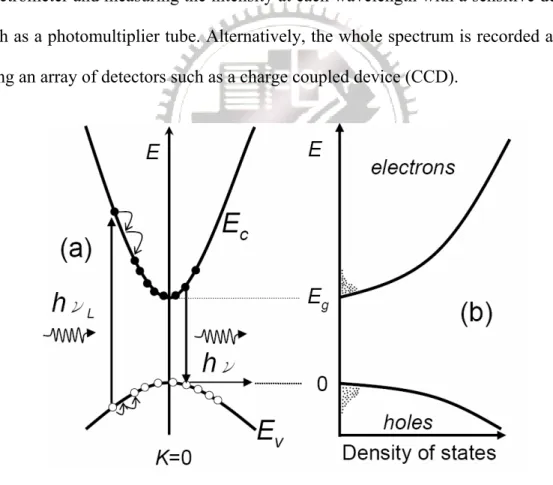
(36) The band diagram corresponding to the photoluminescence process in a direct gap material is given in Figure 2.1(a). Photons are absorbed from an excitation source such as a laser or lamp, and this injects electrons into the conduction band and holes into the valence band. This will be possible if the frequency νL of the source is chosen so that hνL is greater than Eg. It is apparent from Figure 2.1(a) that the electrons are initially created in states high up in the conduction band. The electrons do not remain in these initial states for very long, because they can lose their energy very rapidly by emitting phonons. This process is indicated by the cascade of transitions within the conduction band shown in Figure 2.1(a). Each step corresponds to the emission of a phonon with the correct energy and momentum to satisfy the conservation laws. The electron-phonon coupling in most solids is very strong and these scattering events take place on time scales as short as 100 fs (10-13s). This is much faster than the radiative lifetimes which are in the nanosecond range, and the electrons are therefore able to relax to the bottom of the conduction band long before they have had time to emit photons. The same conditions apply to the relaxation of the holes in the valence band. After the electrons and hole have relaxed as far as they can by phonon emission, they must wait at the bottom of the bands until they can emit a photon or recombine non-radiatively. This leaves time to form thermal distributions, as sketched in Figure 2.2(b), and the shading indicates the occupancy of the available states. These occupancy factors can be calculated by applying statistical physics to the electron and hole distributions.. (ii) Photoluminescence spectroscopy. Photoluminescence spectroscopy is mainly used as a diagnostic and development tool in semiconductor research. The usual goal is to develop electroluminescent devices 34.
(37) such as light-emitting diodes and lasers. This is usually only achieved after the emission mechanisms have been studied in detail using photoluminescence spectroscopy. Photoluminescence spectra can be recorded with an experimental arrangement such as the one shown in Figure 2.2. The sample is mounted in a variable temperature cryostat and is illuminated with a laser or bright lamp with photon energy greater than Eg. If a liquid helium cryostat is used, sample temperatures from 2 K upwards are easily obtained.. The luminescence is emitted at. lower frequencies and in all directions. A portion is collected with a lens and focused onto the entrance slit of a spectrometer. The spectrum is recorded by scanning the spectrometer and measuring the intensity at each wavelength with a sensitive detector such as a photomultiplier tube. Alternatively, the whole spectrum is recorded at once using an array of detectors such as a charge coupled device (CCD).. Figure 2.1: (a) Schematic diagram of the processes occurring during photoluminescence in a direct gap semiconductor after excitation at frequency. (b) Density of states and level occupancies for the electrons and holes after optical excitation.. 35.
(38) Figure 2.2: Experimental arrangement used for the observation of photoluminescence spectra.. 2.2 Material fabrication. 2.2.1 ZnO thin films formation. The ZnO thin films (~100 nm) were deposited on 4 inch diameter Si (001) substrates buffered with SiO2 and Si3N4 and without inter-layers by radio-frequency (RF) magnetron sputtering using 99.99% ZnO as the target. The growth chamber was evacuated by a turbo pump and mechanical pump. The gas mole ratio of oxygen to 36.
(39) argon (OMR) was varied in the range of 0-72%. Silicon substrates were cleaned by usual semiconductor technology before loading into the chamber. Sputtering conditions were optimized at a substrate temperature of 50˚C, RF power of 50W, sputtering pressure of 10mTorr and sputtering time of 30-40 minutes. The buffer layers (inter-layers) were grown by electron evaporation and the thickness of the buffer layers for Si3N4 and SiO2 was measured to be about 10-40 nm, respectively. After sputtering, the as-grown films were cut into several pieces and then annealed at 500, 850 and 1000oC for 20-40 minutes under pure oxygen and nitrogen atmospheres.. 2.2.2 Ions implantation in ZnO films. Ion implantation is a precise method of introducing dopants into a semiconductor and can also be used to create high resistance regions for inter-device isolation. The residual implant damage remaining after annealing appears to have donor-like character. To minimize this damage, it may be necessary to adopt techniques used for other compound semiconductors, such as elevated temperatures during the implant step to take advantage of so-called dynamic annealing in which vacancies and interstitials created by the nuclear stopping process are annihilated before they can form stable complexes. The ZnO films were subsequently subjected to phosphor and nitrogen implantation at room temperature. The phosphor and nitrogen ions with energy of 120 and 80 KeV were injected into the as-grown ZnO films, respectively. The fluences range was from 5 × 10¹² -5 × 1015 cm-2. Based on Rutherford back scattering measurement followed by (the transport of ions in matter) TRIM simulations, the implanted ions distribution in ZnO films forms a nearly perfect Gaussian shape with the peak position at (80±10) nm below the surface. After ions implantation, the 37.
(40) specimens were annealed at 850˚C and 1000˚C for 20 minutes under pure oxygen and nitrogen atmospheres.. 2.2.3 Soft chemical growth and treatment on ZnO nanorods. The ZnO-coated silicon substrates were placed in a solution containing an equimolar (0.01-0.1M) aqueous solution of Zn(NO3)2.6H2O and Hexamethylenetetramine (HMT) and reacted at 75-95oC for 10-24 h. After that, the substrates were removed from the aqueous solutions, rinsed with distilled water, and dried at room temperature overnight. Finally, high quality one-dimensional ZnO nanostructures were developed. The ZnO nanorods were exposed to various plasma atmospheres (nitrogen, oxygen, ammonia, and hydrogen) for 30, 60, 120, 300, and 900 sec by inductively coupled plasma (ICP) system. For the plasma treatment, the substrate temperature, total gas pressure, ICP top power, and bottom power were maintained at different conditions such as Table 2.1.. Table. 2.1: Conditions of plasma treatment on ZnO nanorods.. 2.2.4 Fabrication of one-dimensional nanotube composite device. Figure 2.3 shows the optical microscopy bright-field images of electrode structure made by the electron-beam lithography process. In Figure 2.3 (a), the 16 large 38.
(41) electrode pads are used for wire bonding, connecting to the outside part circuit. In the central part shown in Figure 2.3 (b), several tiny electrode arrays intended to contact nanotubes (or nanowires) are shown. Thin Cr layer (1 nm) is used to enhance the reliable contact and adhesion between the contact metal and SiO2. As we zoomed in Figure 2.3(b), there are four squares in the corners, which are used as alignment markers (Figure 2.3 (c)). For electrical transport measurement, device configuration is shown in Figure 2.4. The nanotube (or nanowire) is embedded in metal electrodes (AuPd alloy) to enhance the electrical coupling between nanotube and electrode. To achieve this aim, predefined coordinate markers are needed to calculate the exact position of selected nanotubes relative to the neighboring coordinate markers. The tolerance shift in our alignment technique is well controlled within around 50 nm. The main advantages of this contact method are to decrease the contact resistance and make possible contact patterns on complicated nanostructures.. (a). Figure 2.3: SEM images of electrode patterns for contacting nanotubes, (a) Large-scale view of pattern. (b) Dark-field image of central part of (a), (c) Bright-field image of (b). Scale bar is 200 µm.. (b). (c) 39.
(42) (a). (b). Figure 2.4: (a) AFM image of coated SWNT embedded in source and drain electrodes. (b) Schematic illustration of coated SWNT device.. 2.3. Characterization of ZnO materials and electrical. transport. The surface morphology of ZnO materials were observed by field emission scanning electron microscopy (FE-SEM). JEOL-6500 FE-SEM system was employed in this study. In order to prevent to damage our samples, we used low voltage (20KeV) to scan these serial images. The transmission electron microscopy (TEM; Philips TECNAI 20) with energy dispersive x-ray spectroscopy (EDS) operated at 200 keV was used for detail crystal analysis. The crystal structures of ZnO films and nanorods were investigated by x-ray diffraction (Siemens, D5000) using Cu Kα radiation and a nickel filter. When an x-ray beam strikes a crystal surface at some angle, a portion is scatted by the layer of atoms at the surface. For optical properties, photoluminescence measurement was performed by the excitation from 325 nm He–Cd laser at room temperature and 10 K. The chemical compositions were examined by x-ray 40.
(43) photoelectron spectroscopys (XPS) after the samples were first sputtered for 90 s to remove the surface containment by Ar ion. Current-voltages (I-V) characteristics curve of the samples was measured by applying dc voltage to the device using a HP-4156 and each datum was averaged by measuring ten times. The electrical properties of the nitrogen-implanted ZnO films were investigated by van der Pauw method room temperature Hall measurements with nonsintered indium contacts and magnetic field of 0.315 T. The precise electrical transport was measured by homemade transport system in Dr. Siegmar Roth’s laboratory in Max-Planck Institute (Stuttgart, Germany). The main components of this system are a desktop computer equipped with a GPIB card and controlled by Labview software (written by Dr. Dirk Obergfell), two Keithely 2400 and one Keithely 230 (voltage source), and a preamplifier. The current is measured using the high sensitivity, low noise current preamplifier. The output voltage is amplified by a conversion factor µ and then read by Keithely 2000 (voltage meter). A RC low-pass filter with a time constant around 0.5 sec is added between gate and voltage source to prevent abrupt potential changes and allow consecutive potential modulation on the one-dimensional nanostructure. The voltage adder is designed to adjust the offset voltage from the preamplifier.. 41.
(44) Chapter 3. Defects engineering on zinc oxide thin films 3.1 Introduction. It is well known that the ultraviolet (UV) emission of ZnO is attributed to exciton-related activities, but for the visible emissions, various mechanisms have been proposed. including. the. involvement. of. zinc. interstitials,[79,80]. oxygen. interstitials,[81,82] zinc vacancies[83,84] and oxygen vacancies.[85,86] In addition, it is known that the sintered ZnO is a nonstoichiometric oxide at room temperature, exhibiting an n-type electrical conductivity due to an excess of the zinc. The zinc excess gives origin to intrinsic donors in ZnO, which can be assigned either to the zinc interstitials (Frenkel defect) [87] or to the oxygen vacancies (Schottky defect) [88]. These two types of point defects have similar electrical properties, being difficult to distinguish between them. However, both point defects exhibit different defect reactions under different annealing temperature and atmosphere. Recently, it has been revealed that the dominant point defect may vary with the annealing temperatures. [89].. During. different. annealing. conditions,. the. crystalline. characteristics of ZnO films would be changed to exhibit various point defects that would affect the luminescent properties.. 3.2 Defects transition in high-orientated ZnO thin films. 42.
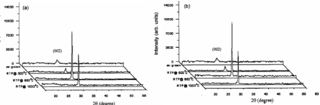
(45) To understand the relation between intrinsic defects and crystallization in ZnO thin films system, we used different manufacturing conditions to figure the defects mechanism out. Figure 3.1 shows the x-ray diffraction patterns of ZnO films sputtered at the OMR of 0%, 5%, 20%, 50% and 72%, and then annealed at 850˚C in N2 and O2. atmospheres. Only a sharp (002) diffraction peak at 2θ ~34.4˚ can be detected for both atmospheres. It indicates that a well-defined and oriented ZnO film has been obtained. However, with an increase of the OMR ratio, the intensity of ZnO (002) diffraction peak was reduced. This reveals that the crystallinity of the ZnO films would be hindered at a high oxygen pressure. As shown in Figure 3.1, although the film crystallinity is not sensitive to the annealing atmosphere, the values (0.22˚, 0.18˚, 0.25˚, 0.28˚ and 0.5˚) of full-width at half maximum (FWHM) for ZnO (002) diffraction peak change with the OMR ratios of 0%, 5%, 20%, 50% and 72%, respectively. The best sputtered ZnO film appears at the OMR of 5% that is probably related to the relative ratio of Zn to ZnO as reported by Fujimura et al.[90] Therefore, the optimum sputtering atmosphere with the OMR of 5% will be used in this work to study the effect of annealing temperature on the film crystallinity unless otherwise noted.. Figure 3.1: XRD patterns of ZnO films as function of OMR conditions after annealing at 850˚C in (a) nitrogen and (b) oxygen atmospheres. 43.
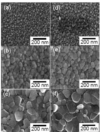
(46) Figure 3.2: XRD patterns of ZnO films sputtered at OMR 5% and annealed at different temperatures in (a) nitrogen and (b) oxygen atmospheres.. Figure 3.2 illustrates that the intensity of the (002) diffraction peak varies with annealing temperature. When the sputtered ZnO films are annealed below 850˚C, it was found that (002) peak intensity increases with annealing temperature up to 850˚C in both N2 and O2 atmospheres because of the enhanced film crystallite and grain size. Above that (850˚C), it decreases. The smallest FWHM value in the ZnO films can be obtained at 850˚C.. This indicates that although a higher annealing temperature can. improve the crystallization of the as-grown ZnO films, as the annealing temperature exceeds 850˚C, especially above 1000˚C, the crystallinity of ZnO films may be deteriorated by either crystalline lattice defects [91] or thermal microstrain due to structure distortion. Therefore, the surface structure and grain morphology in ZnO films will be further modified as illustrated in Figure 3.3, where pill-like structure was formed. The formation of the pill-like structure may be related to the surface free energy and crystalline lattice defects because a large number of zinc element will be vaporized from the ZnO films at such a high annealing temperature. Therefore, in this condition, more point defects would be produced in the ZnO films. For the wide-gap semiconductors, PL emission is one of the most important properties of ZnO. Figure. 44.
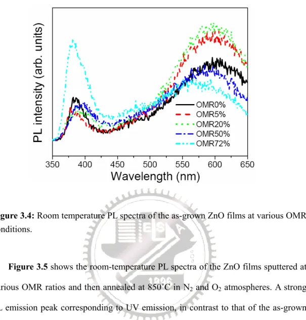
(47) 3.4 shows the room-temperature PL spectra of the as-grown ZnO films sputtered at various OMR conditions. The peak intensity of the deep-level emission around ~600 nm changes with the OMR ratio and the weakest one appears at the OMR of 20%. It can be considered that some of point defects such as oxygen vacancies and zinc interstitials are compensated each other at a certain oxygen pressure. Furthermore, as one can see, along with the decrease in deep-level emission peaks, the peak intensity of the UV emission at ~382 nm increases.. Figure 3.3: SEM surface morphology of OMR5%-treated ZnO films annealed various conditions: (a) 500˚C in N2, (b) 850˚C in N2, (c) 1000˚C in N2, (d) 500˚C in O2, (e) 850˚C in O2, (f) 1000˚C in O2.. 45.
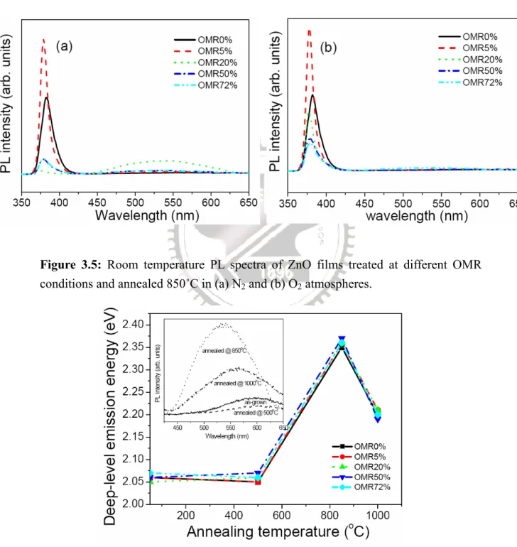
(48) Figure 3.4: Room temperature PL spectra of the as-grown ZnO films at various OMR conditions.. Figure 3.5 shows the room-temperature PL spectra of the ZnO films sputtered at various OMR ratios and then annealed at 850˚C in N2 and O2 atmospheres. A strong PL emission peak corresponding to UV emission, in contrast to that of the as-grown films, appears around 378-382 nm that should be a near band edge emission of ZnO films due to an exciton-related activity.[92] As shown in Figure 3.5(a) for the films annealed in N2 atmosphere, a very stronger UV peak and a relatively low deep-level emission (528 nm) shows up at the OMR of 5%. However, in this condition (annealed in N2 atmosphere), as the ZnO film was sputtered at the OMR of 20%, the UV emission peak becomes weak and a broader deep-level emission appears around 533 nm as compared to that sputtered at other OMR ratios. On the other hand, as the sputtered ZnO films were annealed in O2 atmosphere, Figure 3.5(b) shows that the UV peak not only becomes sharper at the OMR of 5% but also the deep-level emission at ~533 nm is almost barely detected at the OMR of 20%. This phenomenon 46.
數據
![Figure 1.7: TEM images of the as-synthesized ZnO nanobelts, showing uniform morphology [75]](https://thumb-ap.123doks.com/thumbv2/9libinfo/8030224.161368/31.892.158.713.527.935/figure-tem-images-synthesized-nanobelts-showing-uniform-morphology.webp)

+7


Outline
Electrical behaviors
Nanoscience and nanostructures in ZnO materials
Characterization of ZnO materials and electrical transport
Summary
Phosphorous-implanted in ZnO thin films
Characterization of p-type ZnO films
Post-annealing effects on ZnO nanorods
High conductivity ZnO nanorods in hydrogen-plasma
Rectifying behavior of ZnO nanorods by ammonia-plasma
Ultraviolet photoresponse of single ZnO nanorod
相關文件
Teachers may consider the school’s aims and conditions or even the language environment to select the most appropriate approach according to students’ need and ability; or develop
In 2006, most School Heads perceived that the NET’s role as primarily to collaborate with the local English teachers, act as an English language resource for students,
Wang, Solving pseudomonotone variational inequalities and pseudocon- vex optimization problems using the projection neural network, IEEE Transactions on Neural Networks 17
volume suppressed mass: (TeV) 2 /M P ∼ 10 −4 eV → mm range can be experimentally tested for any number of extra dimensions - Light U(1) gauge bosons: no derivative couplings. =>
Define instead the imaginary.. potential, magnetic field, lattice…) Dirac-BdG Hamiltonian:. with small, and matrix
incapable to extract any quantities from QCD, nor to tackle the most interesting physics, namely, the spontaneously chiral symmetry breaking and the color confinement..
• Formation of massive primordial stars as origin of objects in the early universe. • Supernova explosions might be visible to the most
(Another example of close harmony is the four-bar unaccompanied vocal introduction to “Paperback Writer”, a somewhat later Beatles song.) Overall, Lennon’s and McCartney’s
