Transition of carrier distribution from a strained to relaxed state in InGaAs/GaAs
quantum well
P. Y. Wang, J. F. Chen, J. S. Wang, N. C. Chen, and Y. S. Chen
Citation: Journal of Applied Physics 85, 2985 (1999); doi: 10.1063/1.369614
View online: http://dx.doi.org/10.1063/1.369614
View Table of Contents: http://scitation.aip.org/content/aip/journal/jap/85/5?ver=pdfcov
Published by the AIP Publishing
Articles you may be interested in
Microbeam high-resolution x-ray diffraction in strained InGaAlAs-based multiple quantum well laser structures grown selectively on masked InP substrates
J. Appl. Phys. 97, 063512 (2005); 10.1063/1.1862769
Er-related luminescence in Er,O-codoped InGaAs/GaAs multiple-quantum-well structures grown by organometallic vapor phase epitaxy
Appl. Phys. Lett. 80, 1559 (2002); 10.1063/1.1456971
Strained layer (111)B GaAs/InGaAs single quantum well lasers and the dependence of their characteristics upon indium composition
J. Appl. Phys. 89, 4689 (2001); 10.1063/1.1359155
Strain relaxation in In 0.2 Ga 0.8 As/GaAs quantum-well structures by x-ray diffraction and photoluminescence
J. Appl. Phys. 87, 1251 (2000); 10.1063/1.372004
Analysis of abnormal x-ray diffraction peak broadening from InGaAs/GaAs multiple quantum wells
J. Appl. Phys. 82, 4865 (1997); 10.1063/1.366348
[This article is copyrighted as indicated in the article. Reuse of AIP content is subject to the terms at: http://scitation.aip.org/termsconditions. Downloaded to ] IP: 140.113.38.11 On: Thu, 01 May 2014 08:44:04
COMMUNICATIONS
Transition of carrier distribution from a strained to relaxed state
in InGaAs/GaAs quantum well
P. Y. Wang, J. F. Chen, J. S. Wang, N. C. Chen, and Y. S. Chen
Department of Electrophysics, National Chiao Tung University, Hsinchu, Taiwan, Republic of China ~Received 6 July 1998; accepted for publication 17 November 1998!
This work investigates the transition of carrier distribution from the strained to the relaxed state in In0.2Ga0.8As/GaAs quantum well by measuring capacitance voltage and analyzing x-ray diffraction.
According to those results, there is carrier confinement in the In0.2Ga0.8As quantum well with well
thickness less than the critical thickness. Increasing the well thickness beyond the critical thickness leads to a significant carrier depletion around the quantum well. Double-crystal x-ray rocking curves reveal that when InGaAs well thickness increases beyond the critical thickness, the interference pattern disappears and relaxation begins to occur from near the bottom InGaAs/GaAs interface while the top interface still remains strained. Results obtained from the critical thickness determined from x-ray diffraction correspond to the transition of carrier distribution, illustrating that the capacitance–voltage measurement is a rather effective means of determining the critical thickness. © 1999 American Institute of Physics.@S0021-8979~99!01505-4#
The InGaAs/GaAs material system has been extensively applied in electronic and optoelectronic devices. However, due to lattice mismatch between InGaAs and GaAs, there exists a critical thickness of InGaAs, beyond which strain relaxes, accompanied by the generation of misfit disloca-tions, subsequently degrading device performance. There-fore, precisely determining the critical thickness is essential for fabricating high quality optoelectronic devices. Many problems in this system such as strain relaxation, misfit dis-locations, and deep traps have been studied by Hall effect,1,2 double-crystal x-ray diffraction,3 photoluminescence,4,5 deep-level transient spectroscopy,6,7 capacitance–voltage (C – V) method7 and cross-sectional transmission electron microscopy.8–10 However, some of these measurement re-sults are not consistent with each other. For example, the critical thickness reported by Laidig et al.11 from x-ray dif-fraction is more than a factor of 2, i.e., larger than that de-termined from the efficiency of stimulated emission.12In ad-dition, the critical thicknesses determined from different theoretical models, such as the energy balance model of People and Bean13 and the mechanical equilibrium model14 of Matthews and Blakeslee,14 significantly differ from each other. Therefore, the critical thickness and the nature of lat-tice strain and relaxation must be more thoroughly eluci-dated.
Although C – V measurement has been used to examine the carrier distribution, the correlation between the carrier distribution and the critical thickness has not been studied in detail. Therefore, in this investigation, we use C – V mea-surement to investigate the transition of carrier distribution in InGaAs/GaAs quantum well from the strained to the re-laxed state by varying the InGaAs well width. To correlate
these results with strain relaxation, the double-crystal x-ray diffraction is performed to characterize the samples.
Five In0.2Ga0.8As/GaAs quantum well structures with the well width varying from 100 to 1000 Å were grown on n1-GaAs~001! substrates by Varian Gen II molecular beam epitaxy. The InGaAs quantum well, which is located 0.3mm from the surface, was immersed in a GaAs Schottky diode to provide the C – V measurement. Both the InGaAs quantum well and the total 0.6-mm-thick GaAs epilayer were all Si doped with a nominal concentration of 631016 cm23. The entire structure was grown at 550 °C to avert any unneces-sary interruptions in growth which might incorporate some undesired impurities into the interfaces of the quantum well. The thickness and composition of InGaAs were then deter-mined by oscillation of reflection high energy electron dif-fraction. Finally, Schottky diodes were fabricated by evapo-rating Al on samples with a dot diameter of 1500 mm.
Figure 1 summarizes the C – V measurement results for the five samples at reverse bias. These curves can be sepa-rated into two groups. One group consists of samples with small well widths of 100 and 200 Å. The capacitance of these samples falls initially in a well-behaved manner and then levels off at 23 to 25 V and again falls thereafter. Another group consists of samples with large well widths of 300, 400, and 1000 Å. The capacitance of these three samples falls sharply and then levels off at approximately
22 V, implying that the depletion region reaches down to
the substrate when the applied voltage surpasses22 V. Figure 2 presents the corresponding carrier depth pro-files from C – V measurement. A concentration peak obvi-ously appears for samples with small well widths of 100 and 200 Å, implying the existence of carrier confinement in the quantum well. The broader peak for 200 Å reflects its larger
JOURNAL OF APPLIED PHYSICS VOLUME 85, NUMBER 5 1 MARCH 1999
2985
0021-8979/99/85(5)/2985/3/$15.00 © 1999 American Institute of Physics
[This article is copyrighted as indicated in the article. Reuse of AIP content is subject to the terms at: http://scitation.aip.org/termsconditions. Downloaded to ] IP: 140.113.38.11 On: Thu, 01 May 2014 08:44:04
well width. Herein, a numerical simulation resembling that used by Missous and Rhoderick15is undertaken on the C – V and carrier depth profile by solving the Poisson equation. The inset of Fig. 2 displays the simulated ~solid dots! and experimental ~curve! carrier profiles for the well width of 100 Å. Simulation results can correlate well with the carrier profiles for well widths of 100 and 200 Å with a good accu-racy, indicating that the quantum structures are of high qual-ity for both cases.
Figure 2 also reveals markedly different carrier distribu-tions for well widths of 300, 400, and 1000 Å. Instead of containing peaks, their curves illustrate that the carriers in the quantum well are depleted. This carrier depletion is so pervasive that it goes beyond the quantum well region and spreads to GaAs layers on both sides. This carrier depletion is possibly attributed to the fact that when the InGaAs thick-ness increases to 300 Å, misfit dislocations occur from strain relaxation. These misfit dislocations act like traps which de-plete carriers both in the quantum well and the GaAs layers around it. If this assumption is valid, the critical thickness for In0.2Ga0.8As quantum well should range between 200 and
300 Å. To verify this assumption, double-crystal x-ray
rock-ing curves along~004! diffraction are taken for all samples, thereby allowing us to directly measure the lattice spacing in the growth direction.
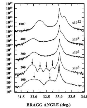
Figure 3 summarizes the results of the double-crystal x-ray diffraction. The GaAs peaks are set to approximately 33° on the angular scale. For the cases of 100 and 200 Å, the interference pattern can be clearly observed where peak po-sitions correlate with our calculation as denoted by the ar-rows in Fig. 3, showing a good interface flatness of the quan-tum well. The interference peak positions are calculated as follows. For the case of 200 Å, while considering a slight variation of well width during the growth, we substitute a fitted well width of 200.63 Å into d of equation 2d sinu
5nl, ~where l51.54 Å!, u is calculated to be 32.76°, 32.50°, 32.24°, and 31.98° for n5141, 140, 139, and 138, respectively. These values closely resemble the experimental values of 32.75°, 32.50°, 32.26°, and 31.94° in Fig. 3. For the case of 100 Å, using d5100 Å, the calculated u are 32.62° and 32.09° for n570 and 69, which closely resemble the experimental values of 32.68° and 32.04°. However, when InGaAs thickness increases to 300 Å, the interference pattern disappears and only the InGaAs peak is visible. The InGaAs peaks are at nearly the same angular position for 300 and 400 Å. However, when the well width increases to 1000 Å, the InGaAs peak moves to the right, showing the relax-ation of the InGaAs layer.
Figure 3 also reveals that when InGaAs thickness in-creases to 300 Å, a bump on the right shoulder of the GaAs peak appears. The appearance of this bump suggests that a strained GaAs layer exists whose lattice is compressed in the growth direction. Figure 3 reveals that this bump moves to the right with an increasing InGaAs thickness. This observa-tion implies that the compression of this strained GaAs layer in the growth direction is attributed to the relaxation of the
FIG. 1. The C – V measurement of In0.2Ga0.8As/GaAs strain quantum well
structures with well thickness 100, 200, 300, 400, and 1000 Å.
FIG. 2. The corresponding carrier concentration depth profiles for In0.2Ga0.8As/GaAs quantum well structures with well width 100, 200, 300,
400, and 1000 Å. Shown in the inset are the simulated ~solid dots! and experimental~curve! carrier profiles for the well width of 100 Å.
FIG. 3. Double-crystal x-ray rocking curves along ~004! diffraction for In0.2Ga0.8As/GaAs quantum well structures with well width 100, 200, 300,
400, and 1000 Å. The GaAs peaks are set to be about 33° on the angular scale.
2986 J. Appl. Phys., Vol. 85, No. 5, 1 March 1999 Wanget al.
[This article is copyrighted as indicated in the article. Reuse of AIP content is subject to the terms at: http://scitation.aip.org/termsconditions. Downloaded to ] IP: 140.113.38.11 On: Thu, 01 May 2014 08:44:04
InGaAs layer. This feature suggests that when the InGaAs layer relaxes, it starts presumably from the InGaAs/GaAs bottom interface while the top interface still remains strained. A previous investigation using photoluminescence measurement observed a similar phenomenon.5 If this is valid, the lattice constant parallel to the interface ai should
be the same for the top GaAs and the relaxed InGaAs layer. Therefore, the top GaAs layer is compressed along the growth direction, providing the bump on the shoulder of GaAs peak. To prove this assumption, this study also calcu-lates the peak position of the bump for the 1000 Å case. The elastic constants for InGaAs are calculated from the In com-position using C1158.32931011, C1254.52631011dyn/cm2
for InAs and C11511.8831011, C1255.3831011 dyn/cm2
for GaAs. From the peak position ~32.25°! of InGaAs in Fig. 3, the lattice constant of the InGaAs perpendicular to the interface a'(InGaAs) is 5.7738 Å. According to a'
5(12sSTf )a, 16
the lattice mismatch f is determined to be 7.256231023, where sST52C12/C11 and a denotes the
natural ~unstrained! lattice constant. Next, from ai5(1 1 f )a, ai(InGaAs) is calculated to be 5.6926 Å. Because the
fact that the top GaAs is expanded by InGaAs, from ai(top GaAs)5ai(InGaAs) and proceeds in a similar manner,
a'(top GaAs) is calculated to be 5.6175 Å. Therefore, the bump should appear at 33.26°, considering the influence of the main GaAs peak, which is reasonably close to the experi-mental value of 33.21° as shown in Fig. 3.
The appearance of the bump for the case of 300 Å indi-cates that the InGaAs layer is partially relaxed. This relax-ation is accompanied by the generrelax-ation of misfit dislocrelax-ations which degrade the structure quality, as evidenced by the ab-sence of an interference pattern. From these results, we can infer that the critical thickness for InGaAs quantum well ranges between 200 and 300 Å. Notably, this information is difficult to obtain merely by the peak separation between GaAs and InGaAs. Our results further indicate that the cal-culated perpendicular lattice constant of a strained InGaAs
~without relaxation! is in close proximity to the InGaAs
peaks for the cases of 300 and 400 Å. This is likely attributed to a lack of sensitivity of x-ray measurement for samples with small relaxation. Figure 3 depicts a slight variation in the InGaAs peaks for 300 and 400 Å, which is likely attrib-uted to a variation of In composition during the sample
growth. The critical thickness~between 200 and 300 Å! de-termined herein corresponds to the transition of carrier dis-tribution from confinement to depletion, as indicted from C – V measurement.
In summary, this work investigates the correlation be-tween the carrier distribution and critical thickness in InGaAs/GaAs quantum well. According to those results, a transition from carrier confinement to depletion occurs when InGaAs thickness increases beyond the critical thickness. This finding suggests that the capacitance–voltage measure-ment is a very sensitive technique for determining the critical thickness. X-ray diffraction results indicate that a clear inter-ference pattern can be observed when the InGaAs thickness is below the critical thickness. When the InGaAs layer ex-ceeds the critical thickness, relaxation begins to occur from near the bottom InGaAs/GaAs interface while the top inter-face still remains strained. The critical thickness determined herein is consistent with the critical thickness reported by Fritz et al.1 from low temperature Hall-effect measurement and photoluminescence microscopy.
The authors would like to thank the National Science Council of the Republic of China for financially supporting this research under Contract No. NSC-87-2112-M-009-022.
1
I. J. Fritz, P. L. Gourley, and L. R. Dawson, Appl. Phys. Lett. 51, 1004
~1987!.
2I. J. Fritz, S. T. Picraux, L. R. Dawson, and T. J. Drummond, Appl. Phys.
Lett. 46, 967~1985!.
3
P. J. Orders and B. F. Usher, Appl. Phys. Lett. 50, 980~1987!.
4M. J. Joyce, M. Galand, and J. Tann, J. Appl. Phys. 65, 1377~1989!. 5M. Gal, P. J. Orders, B. F. Usher, M. J. Joyce, and J. Tann, Appl. Phys.
Lett. 53, 113~1988!.
6
G. P. Watson, D. G. Ast, T. J. Anderson, B. Pathangey, and Y. Hayakawa, J. Appl. Phys. 71, 3399~1992!.
7Y. Uchida, H. Kakibayashi, and S. Goto, J. Appl. Phys. 74, 6720~1993!. 8J. Zou and D. J. H. Cockayne, Appl. Phys. Lett. 70, 3134~1997!. 9J. Zou and D. J. H. Cockayne, J. Appl. Phys. 73, 619~1993!. 10
R. H. Dixon and P. J. Goodhew, J. Appl. Phys. 68, 3163~1990!.
11W. D. Laidig, C. K. Peng, and Y. F. Lin, J. Vac. Sci. Technol. B 2, 181
~1984!.
12N. G. Anderson, W. D. Laidig, and Y. F. Lin, J. Electron. Mater. 14, 187
~1985!.
13
R. People and J. C. Bean, Appl. Phys. Lett. 47, 322 ~1985!; 49, 229
~1986!.
14J. W. Matthews and A. F. Blakeslee, J. Cryst. Growth 27, 118~1974!. 15M. Missous and E. H. Rhoderick, Solid-State Electron. 28, 233~1985!. 16
P. Bhattacharya, Semiconductor Optoelectronic Devices~Prentice–Hall, Englewood Cliffs, NJ, 1994!, p. 21.
2987
J. Appl. Phys., Vol. 85, No. 5, 1 March 1999 Wanget al.
[This article is copyrighted as indicated in the article. Reuse of AIP content is subject to the terms at: http://scitation.aip.org/termsconditions. Downloaded to ] IP: 140.113.38.11 On: Thu, 01 May 2014 08:44:04