國立交通大學
顯示科技研究所
碩 士 論 文
低溫複晶矽薄膜電晶體的電容特性及模擬
Analysis and Simulation of
Capacitance Characteristic in Low-Temperature
Polycrystalline Silicon Thin-Film Transistors
研 究 生:蘇旻君
指導教授:冉曉雯 博士
低溫複晶矽薄膜電晶體的電容特性及模擬
Analysis and Simulation of
Capacitance Characteristics in Low-Temperature
Polycrystalline Silicon Thin-Film Transistors
研 究 生:蘇旻君 Student:Min-Chun Su
指導教授:冉曉雯 博士 Advisor : Dr. Hsiao-Wen Zan
國 立 交 通 大 學
顯示科技研究所
碩 士 論 文
A Thesis
Submitted to Institute of Display
College of Electrical and Computer Engineering National Chiao Tung University
in Partial Fulfillment of the Requirements for the Degree of
Master In Display July 2008
HsinChu, Taiwan, Republic of China.
低溫複晶矽薄膜電晶體的電容特性及模擬
研究生: 蘇旻君 指導教授:冉曉雯 博士
國立交通大學
顯示科技研究所碩士班
摘要
近年來,低溫複晶矽薄膜電晶體已引起大量的研究,其應用相當廣泛。低溫 複晶矽薄膜電晶體在面板技術的應用上,由於具有高遷移率,而有機會整合面板 周邊電路,實現系統面板的目標。當低溫複晶矽薄膜電晶體應用為驅動電路時, 交流信號將操作於閘極。因此低溫複晶矽薄膜電晶體對於元件在交流信號下的頻 率響應就具有相當大的重要性。 在本篇論文中,使用準分子雷射製作低溫複晶矽薄膜電晶體,利用阻抗分析 儀,量測電容-電壓和電容-頻率來研究準分子雷射製作的複晶矽薄膜電晶體。 調變在不同準分子雷射能量密度下的複晶矽薄膜品質,觀察電容在不同的閘極偏 壓下對頻率的變化。改變元件尺寸大小及製程步驟,來觀察元件特性的變化。由 於複晶矽薄膜的品質不同,在複晶矽結晶顆粒較小的時候,可以利用先前研究的 模型或是RPI 模型,考慮膜內單一能階的缺陷,來解釋元件的電容特性。當複晶矽的結晶顆粒逐漸增大,先前研究的模型或是RPI 模型已經不能解釋 C-f 曲線呈 現斜直線的現象,單一能階的缺陷已經不能解釋,應由連續能階的缺陷去解釋。
利用 Seto 模型的觀念,考慮晶粒邊界的能障對載子的影響,成功地建立一個模
Analysis and Simulation of Capacitance Characteristic in Low-Temperature
Polycrystalline Silicon Thin-Film Transistors
Student: Min-Chun Su Advisor: Dr. Hsiao-Wen Zan
Institute of Display
National Chiao Tung University, Hsinchu, Taiwan
Abstract
In recent years, low temperature polycrystalline silicon thin-film transistors (poly-Si TFTs) have been investigated extensively for their wide applications. Poly-Si TFTs have been studied extensively for their application on system-on-panel (SOP) technology due to the high mobility. The low temperature poly-Si TFTs are operated under gate alternating current signal. Therefore, the studies of frequency response of low temperature poly-Si TFTs under gate alternating signal become very important.
In this thesis, the low temperature polycrystalline silicon TFTs fabricated by the excimer laser annealing (ELA). To research the characteristics of ELA poly-Si TFTs is analyzing the capacitance-voltage (C-V) and capacitance-frequency (C-f) by using impedance analyzer. Here, by adjusting different poly silicon crystalline film qualities due to different excimer laser energy densities, the variation of the measured capacitance under different gate biases is observed. We change the dimension of poly-Si TFTs and the fabrication process to observe the characteristic of devices. As
poly-Si grain is small, the capacitance characteristics of the poly-Si TFTs can be described by RPI model or the pre-studies which considering the mono-energetic (single energy level) of the trap. As the grain size becomes larger, RPI model or the pre-studies can not be applied to the case which C-f curve is sideling straight. The mono-energetic response is not able to fit experiment result, and we need to specify a continuous-distributed response time of the trap. Using the Seto’s model, we consider the energy barrier of the grain boundary, and the influence of the carriers. We make a new simulation to express the C-f curve successfully.
Acknowledgement
時光飛逝,短短的兩年碩士生活一下子、一眨眼就過去了。在此,我要先感 謝我的指導教授-冉曉雯博士。在我學習的日子裡,由於老師熱誠的教學,教導 了我們許多處事應有的態度,而且提供了一個良好的資源與環境,使我於研究期 間獲得許多寶貴的知識;在論文的研究主題上,感謝老師用心的指導,在我迷惘 的時候指引方向,讓我看得更清楚,這些讓我受益良多。感謝口試委員,劉柏村 老師、李柏璁老師與孟心飛老師對論文的建議,使得這篇論文更為完善。 感謝實驗室的博班學長們,國錫學長、士欽學長、政偉學長和明達學長,感 謝你們在這段時間的幫助,解決了許多課業上的問題以及實驗上的疑惑;感謝畢 業的學長姐們,志宏、育敏、光明、文馨、而康、廷遠、德倫、芸嘉、皇維和睿 志,感謝你們將實驗室的氣氛營造的如此歡樂,緩和了研究遇到瓶頸時的煩悶; 感謝同屆的夥伴們,俊傑、和璁、權陵、亭洲、武衛和志宇,一起為了實驗失敗 而煩惱、為了結果而不停的討論、為了報告用英文而緊張,彼此互相勉勵,努力 地朝著「畢業」這個目標前進;感謝實驗室的學弟妹們,歐陽、玉玫、建敏、繁 琦、芳弘、鈞銘、淑鈴、達欣、煥之和威豪,你們讓實驗室就像個大家庭一樣, 使實驗室的氣氛更加溫暖。 感謝好友們,淳伊、慈殷、心華和孟樺,謝謝你們的關心以及一直以來的支 持;感謝倫豪,在我需要幫助時、感到落寞時,總是給我不斷的鼓勵與信心,這 是讓我向前的動力;最後我要感謝我的家人,親愛的爸爸、媽媽和阿亮,在人生的旅途上,因為有你們的愛,所以讓我變得更加成熟,能勇敢地去面對每個挑戰, 感謝你們從小到大的關懷與照顧。
僅以這篇論文,獻給我的老師、好友與家人。
旻君 2008 夏 于新竹
Contents
Chinese Abstract Ⅰ English Abstract Ⅲ Acknowledgement Ⅴ Contents Ⅶ Table Captions Ⅸ Figure Captions Ⅹ Chapter 1. Introduction 11-1 Introduction of the polycrystalline silicon thin-film transistor 1
1-2 Introduction of Seto’s mode 3
1-3 Introduction of the RPI C-V model of the poly-Si TFT 6
1-4 Motivation 8
1-5 Thesis outline 8
Figure 10 References 12
Chapter 2. Experimental Procedures 16
2-1 Fabrication processes of LTPS poly-Si TFT 16
2-2-1 Instrument 17
2-2-2 Setup instrument for the C-V and C-f measurement 19
Figure 20
References 23
Chapter 3. Results and Discussions 24
3-1 The analysis of the C-V curve 24
3-1-1 Poly-Si TFTs with various channel length and LDD length 24
3-1-2 Poly-Si TFTs with the fabrication process, GI-Clean step 26
3-1-3 C-V measurement with various osc level 28
3-2 The analysis of the C-f curve 30
3-2-1 Poly-Si TFTs with various laser energy 30
3-2-2 A new simulation method for C-f curve 31
Table 36
Figure 38
Reference 51
Table Captions
Chapter 3.
Table.1 The relationship between laser energy density and average grain size which is
defined SEM images after secco etching. 36
Table.2 The parameter values of the new C-f simulation for the W/L=600μm/6μm
Figure Captions
Chapter 1.
Fig.1-2-1 One-dimensional energy band diagram in polycrystalline material. The grain size is assumed to be constant. At grain boundaries, defects are
electrically active. 10
Fig.1-2-2 Simplified distribution of charges within the grain and at grain boundaries. At grain boundaries, the trap state density is defined per
surface unit, while ND is a doping volume concentration. 10
Fig.1-2-3 Transmission line model proposed by RPI. 11
Fig.1-2-4 Equivalent circuit model for SPICE transient and small signal
Chapter 2.
Fig.2-1-1 The schematic cross sectional view of p-type ELA poly-Si TFT without
LDD structure. 20
Fig.2-1-2 The schematic cross sectional view of n-type ELA poly-Si TFT with
LDD structure. 20
Fig.2-1-3 The device fabrication process of n-type TFT with LDD structure. 21 Fig.2-2-1 Circuit diagrams of C-V measurement. In CG-S,DG measurement, drain
was connected to the ground terminal of the measuring instrument, but in CG-S,DF measurement, the drain electrode was floated. Similarly, CG-D,SG and CG-D,SF. CG-DS or CG-SD is the capacitance between the gate and the
source-drain connected together. 22
Fig.2-2-2 CG-SD, CGS-DF and CGD-SF versus VG characteristic of poly-Si TFTs with
Chapter 3.
Fig.3-1-1(a) C-V curves of ELA n-type poly-Si TFT, W/L=600µm/6µm, frequency is
from 10 kHz to 1 MHz, and ELA laser energy is 380 mJ/cm2. 38
Fig.3-1-1(b) C-V curves of ELA n-type poly-Si TFT, W/L=600µm/600µm, frequency
is from 1 kHz to 100 kHz, and ELA laser energy is 380 mJ/cm2. 38
Fig.3-1-2 C-V curves of ELA n-type poly-Si TFT with various channel length at 10
kHz. 39 Fig.3-1-3 Capacitance-channel length curve of ELA n-type poly-Si TFT at large
gate voltage. 39
Fig.3-1-4 C-V curves of ELA n-type poly-Si TFT with various LDD length at 10
kHz. 40 Fig.3-1-5 Capacitance-LDD length curve of ELA n-type poly-Si TFT at large g
ate voltage. 40
Fig.3-1-6(a) C-V curves of ELA p-type poly-Si TFT, W/L=600μm/6μm, and frequency from 10 kHz to 1 MHz. The red curves stand for the device with doing GI-clean process. The blue curves stand for the device
without doing GI-clean process. 41
Fig.3-1-6(b) C-V curves of ELA n-type poly-Si TFT, W/L=600μm/6μm, LDD length=0.75μm, and frequency from 10 kHz to 1 MHz. The red curves
stand for the device with doing GI-clean process. The blue curves stand
for the device without doing GI-clean process. 41
Fig.3-1-7 C-V curves of ELA n-type poly-Si TFT with various osc level at 10 kHz.
42
Fig.3-1-8 The schematic of the moving Fermi level on the electron density of state-energy curve. (a) at small gate voltage (b) at large gate voltage
42
Fig.3-2-1 C-V curves of ELA n-type poly-Si TFT, W/L=600µm/6µm, frequency is
from 10 kHz to 1 MHz, and ELA laser energy is (a) 380 mJ/cm2, (b) 360
mJ/cm2, and (c) 340 mJ/cm2. 43
Fig.3-2-2 C-f curves of ELA p-type poly-Si TFT, W/L=600μm/6μm, with various
eximer laser energy. 44
Fig.3-2-3 C-f curves of various kind of TFT. (a) α-Si MIS, W/L=500μm/1000μm.
(b) α-Si TFT, W/L=600μm/4.5μm. (c) poly-Si TFT, W/L=600μm/6μm,
with laser energy density=380mJ/cm2. 44
Fig.3-2-4 The curves are simulated by using the RPI model. The device is ELA
n-type poly-Si TFT with laser energy density, 380mJ/cm2. 45
Fig.3-2-6 The curve of the energy band with various gate voltages for grain size of
600 nm. 47
Fig.3-2-7 The schematic for the step of this new simulation. 48
Fig.3-2-8(a) The curves are calculated by using this new simulation for small grain.
49
Fig.3-2-8(b) The curves are calculated by using this new simulation for large grain.
49
Fig.3-2-9(a) The measured curves and the simulated curves for small grain. 50 Fig.3-2-9(b) The measured curves and the simulated curves for large grain. 50
Chapter 1
Introduction
1-1 Introduction of polycrystalline silicon thin-film transistors
Polycrystalline silicon thin film transistors (poly-Si TFTs) have attracted more attention because of their widely applications on active matrix liquid crystal displays (AMLCDs) [1.1]-[1.4], organic light-emitting displays (OLEDs), three-dimensional (3D) integrated circuits [1.5]-[1.7] and memory devices such as dynamic random access memories (DRAM’s) [1.8], static random access memories (SRAM’s) [1.9], electrical programming read only memories (EPROM’s) [1.10], electrical erasable programming read only memories (EEPROM’s) [1.11], and charge coupled device (CCD). Undoubtedly, poly-Si TFT technology is the most promising approach.
Unlike amorphous silicon (a-Si) TFT’s or organic TFTs, poly-Si TFT’s have
much higher carrier mobilitywhich usually exceeds 100 cm2/V-sec by present mature
technology. The superior carrier mobility is essential to integrate Poly-Si TFT’s successfully and peripheral driving circuits [1.9] on the same panel to reduce the assembly complexity and cost. Furthermore, because of the higher mobility, the dimension of the poly-Si TFTs can be designed smaller to get larger aperture ratio in each pixel and higher turn-on current, which allows a higher panel resolution.
However, there are still some problems existed in Poly-Si TFT’s. There are a lot of defects at the disordered grain boundaries of poly-Si films which degrade device performance severely. The performance of poly-Si TFTs is strongly influenced by grain boundary in the channel region. In order to make high performance poly-Si TFTs, low-temperature technology is required for the commercial flat-panel displays (FPD) on inexpensive glass substrate, whereas the maximum processing temperature needs to be kept below than 600 °C [1.12]. There are several techniques have been proposed and developed [1.12]-[1.14] to manufacture the LTPs film on glass or plastic substrate: solid phase crystallization (SPC), sequential lateral solidification (SLS), excimer laser crystallization (ELC), and metal-induced lateral crystallization (MILC). Because of the recrystallization, process will influence the quality of Poly-Si films and it will influence the device performance of Poly-Si TFT’s spontaneously. Thus, the roughness and uniformity of poly-Si film are important issues that may degrade the electrical characteristics if the laser energy is not accurately controlled.
In conclusion, the main limitation of poly-Si TFTs is their instability for various kinds of applications, associated with the trap states. To overcome this inherent disadvantage of poly-Si films, many researches have been focused on modifying or eliminating these grain boundary traps. Hydrogenation is a method for reducing the trap density in poly-Si film [1.15]-[1.17]. As the number of trapped carriers decreases,
the potential barrier associated with the grain boundary also decreases and enhances the characteristics of poly-Si TFTs.
1-2 Introduction of Seto’s model
As previously mentioned, the poly-Si material contains some grain boundaries. The device characteristics of poly-Si TFTs are strongly influenced by the grain structure in poly-Si film. J.Y Seto proposed a new model for the electrical properties and the carrier transport in poly-Si TFTs [1.18]. The Seto’s model is based on the following assumptions:
z Poly-Si film has small grain size,
z The single crystalline silicon energy band structure is assumed to be applicable inside the crystallites,
z Doping concentration in poly-Si is uniform, z All the doping atoms are ionized,
z All the grains have the same size,
z The representation is mono-dimensional, z The grain boundaries have no thickness,
z The defects are carrier traps that are located in grain boundaries.
The trap concentration is defined per surface unit. The trap is assumed to be initially neutral and become charged by trapping carriers,
z The traps are acceptors in the n-type and donors in the p-type semiconductor. z The trap energy level is unique and located more or less in the middle of the
forbidden band.
In this model, it is assumed that the poly-Si material is composed of a linear chain of identical crystallite having a grain size LG and the grain boundary trap
density NT, as Fig. The charge trapped at grain boundaries is compensated by
oppositely charged depletion regions surrounding the grain boundaries. This model is based on the calculation of energy barrier at grain boundaries, which affects the transport f electrons in the film. To calculate the energy barrier, the simplest way consists of solving the Poisson’s equation in the grain. We consider the different following parameters:
z X, extension of the space charge region, z ND, donor doping atom concentration,
z NTA, acceptor like trap surface density at grain boundaries,
z ε0, permittivity in vacuum,
z εs, semiconductor permittivity,
z LG, size of the grain,
z V, the electrostatic potential, z x, the position coordinate,
The distribution of the charges in the material is schematically described in Fig.1-2-1.
In the space charge region,
2 0<x< X , 0 2 2 ε εs D qN dx V d =− (1) Out of the space charge region,
2 2 G L x X < < , 2 0 2 = dx V d (2) At the border of the space charge region, the electric field is null: [ ] 0
2 = X dx dV 2 0<x< X : ) 2 ( . 0 0 x X qN const x qN dx dV s D s D + = − − = ε ε ε ε , ( ) 2 (2 ) (2) 2 0 X V x X qN x V s D − + − = ε ε 2 2 G L x X < < : ) 2 ( ) (x V X V =
And the energy barrier height (EB) is defined as the energy difference between the positions x=0 and 2 X x= , 2 0 2 0 8 ) 2 ( 2 )] 2 ( ) 0 ( [V V X qN X qN X V s D s D B=− − = εε = ε ε (3)
The value of X has to verify for the electrical neutrality of the global material, which
means , is the ionized part of . The Seto’s model defines a
critical concentration ( ), which corresponds to this limit:
− += TA D N XqN NTA− NTA * D N G TA D G G L N N L X L X = → = → = * 2 2 (4)
For a fixed trap density, if the effective doping concentration is higher than the critical concentration, the space charge extension is lower than the crystallite site.
G TA D D L N X N N > * : = and D TA s B N N q V 2 0 8ε ε = (5) G D D N X L N < * : = and 2 0 8 s G D B L qN V ε ε = (6)
ch th G ox qt V V C n= ( − ) (7)
where tch is the thickness of the inversion layer.
1-3 Introduction of the RPI C-V model of the poly-Si TFT
In RPI AC models, the grain boundary and intra-grain trap states in poly-Si result the gate to source/drain capacitance (CG-SD) of a TFT in a function of measurement frequency. Here, the source and drain terminals of an n channel TFT have been shorted to ground, and a small signal is applied to the gate of the device. For a signal frequency of 10 kHz, CG-SD increases from approximately zero to the gate oxide capacitance (Cox) as VGS is increased. The frequency dispersion phenomenon can be comprehended by considering the transmission line model that is illustrated in Fig.1-2-1. A typical analysis of the effective circuit model forms complex impedance between the gate and source/drain terminals which depends on different frequencies. For single crystalline silicon transistors, the impedances are very small due to high mobility. Therefore the capacitance is almost independent of frequency.
In the RPI models, the small signal equivalent circuit model is shown in Fig.1-2-4 [1.19], where the gate resistors, rsx and rdx, are in series with the capacitances and approximate the distributed nature of the structure. For zero drain and source bias, the device is symmetric, rsx = rdx and Csx = Cdx. Based on a circuit analysis of Fig.1-2-4 where rsx = rdx and Csx = Cdx, the effect gate to source/drain
capacitance, CG-SD, is given as a function of frequency, ω, by 1 ) ( 2 2+ = − sx sx sx SD G C r C C ω . (8)
At very low frequency, rsx and rdx have little effect, and CG-SD approaches the frequency independent value of 2Csx. Accordingly, for zero drain bias, Csx = Cdx is given by ] ) ( exp[ 2 1 2 1 2 ' T c th GS ox SD G sx V V V LW C C C η − − + × = = − . (9)
ηc is the capacitance ideality factor, VT is the thermal voltage and the other symbols have their usual meanings.
Besides, previous research also referred to later flow transmission line model [1.19][1.20], and introduced the influence of depletion capacitance (CD). These statements indicated the variation of measured capacitances with different frequencies primarily arises from a frequency response associated with the later flow of carriers into and out of the channel from adjacent source and drain region.
However, the defects existed at the interface between gate oxide and poly-Si film, the grain boundary defects and the intra-grain defects are other factors to affect the device performance which are likely to respond to the small ac signal. Because of the response time of these defects, the measured capacitance is also a function of frequency in the depletion region. Therefore, the effect of trap capacitance (Ct) should be taken into account, where Ct is in parallel with CD.
1-4 Motivation
The large area electronics or the flat-panel displays comprised of poly-Si TFTs are widely used all over the world. Most of the previous studies have focused on the analysis of the defect density within the energy band-gap, the dependence of mobility on different biases, film qualities, environment temperatures, and the extraction of effective parasitic resistance by drain current-voltage measurement.
In addition, in recent years, the fabrication technology of poly-Si TFTs have been improved a lot, and the poly-Si grain become larger. About the RPI model or the pre-studies are not appropriate for the devices with large grain, so we want to make a new simulation for these devices.
1-5 Thesis outline
This thesis is organized into the following manner.
In Chapter 1, the various kinds of applications, the advantages and the disadvantages of poly-Si TFTs, and several popular laser crystallization technologies are introduced in a brief overview of the poly-Si TFT technology. Then, Seto’s model, RPI model of poly-Si TFTs and the other background studies are discussed briefly. Finally, the motivation of this work to study the capacitance modeling of poly-Si TFTs is expressed.
In Chapter 2, detailed fabrication processes of ELA poly-Si TFTs, and the instruments which we use to measure are introduced, respectively. The measuring conditions are described concisely.
In Chapter 3, the discussion is divided into two parts: First, the phenomena of the C-V curves are analyzed. Second, the phenomena of the C-f curves are analyzed.
Figure
Fig.1-2-1 One-dimensional energy band diagram in polycrystalline material. The grain size is assumed to be constant. At grain boundaries, defects are electrically active.
Fig.1-2-2 Simplified distribution of charges within the grain and at grain boundaries. At grain boundaries, the trap state density is defined per surface unit, while ND is a doping volume concentration.
Fig.1-2-3 Transmission line model proposed by RPI.
Source Drain
Gate
Fig.1-2-4 Equivalent circuit model for SPICE transient and small signal simulations
Reference
[1.1] A. G. Lewis, I-W. Wu, T. Y. Huang, A. Chiang, and R. H. Bruce, “Active Matrix Liquid Crystal Display Design Using Low and High Temperature Processed Polysilicon TFTs’’, in IEDM Tech. Dig., pp.843-846, 1990
[1.2] R. G. Stewart, S. N. Lee, A. G. Ipri, D. L. Jose, D. A. furst, S. A. Lipp, and W. R. Roach, “A 9V Polysilicon LCD with Integrated Gray-Scale Drivers”, Soc. Information Display, Tech. Dig., pp.319-322, 1990
[1.3] Y. Matsueda, M. Ashizawa, S. Aruga, H. Ohshima, and S. Morozumi, “New Technologies for Compact TFT LCDs with High-Aperture Ratio’’, soc. Information Display, Tech. Dig., pp.315-318, 1990
[1.4] H. Oshima and S. Morozumi, “Future Trends for TFT Integrated Circuits on Glass Substrates,” IEDM Tech. Dig., 157, 1989
[1.5] S. Zhang, C. Zhu, J. K. O. Sin, J. N. Li, and P. K. Mok, “Ultra-Thin Elevated Channel Poly-Si TFT Technology for Fully-Integrated AMLCD System on Glass”, IEEE Trans. Electron Devices, Vol.47, No.3, pp.569-575, March 2000 [1.6] Z. Meng, M. Wang, and M. Wong, “High Performance Silicon Thin Film
Transistors for System-on Panel Applications”, IEEE Trans. Electron Devices, Vol.47 No.2, pp.404-409, February 2000
Pollack, W. F. Richardson, A. H. Shah, L. R. Hite, R. H. Womack, P. K. Chatterjee, and H. W. Lam, “Characteristics and Three-Dimensional Integration of MOSFET’s in Small-Grain LPCVD Polycrystalline Silicon”, IEEE Solid-State Circuits, Vol.SC-20, No.1, pp.178-201, February 1985
[1.8] T. Yamanaka, T. Hashimoto, N. Hasegawa, T. Tanaka, N. Hashimoto, A. Shimizu, N. Ohki, K. Ishibashi, K. Sasaki, T.Nishida, T. Mine, E. Takeda, and T. Nagano, ”Advanced TFT SRAM Cell Technology Using a Phase-Shift Lithography’’, IEEE Trans. Electron Devices, Vol.42, No.7, pp.1305-1313, 1995
[1.9] S. D. S. Malhi, H. Shichijio, S.K. Banerjee, R. Sundaresan, M. Elahy, G. P. Polack, W. F. Richardaon, A. h. Shah, L. R. Hite, R. H. Womoack, P. K. Chatterjee, and H. W. Lan, “Characteristics and Three-Dimensional Integration of MOSFETs in Small-Grain LPCVD Polycrystalline Silicon’’, IEEE Trans. Electric Devices, Vol.32, No.2, pp.258-281, 1985
[1.10] K. YoShizaki, H. Takahashi, Y. Kamigaki, T.Yasui, K. Komori, and H. Katto, ISSCC Digest of tech. Papers, pp.166, 1985
[1.11] N. D. Young, G. Harkin, R. M. Bunn, D. J. McCullloch, and I.D. French, “The Fabrication and Characterization of EEPROM Arrays on Glass Using a Low-Temperature Poly-Si TFT Process’’, IEEE Trans. Electron Devices,
Vol.43, No.11, pp.1930-1936, 1996
[1.12] S. W. Lee, S. K. Joo, “Low Temperature Poly-Si Thin-Film Transistor Fabricated by Metal-Induced Lateral Crystallization”, IEEE Electron Device Lett., Vol.17, No.4, pp.160-162, April 1996
[1.13] Hiroyuki Kuriyama, Seiichi Kiyama, Shigeru Nouguchi, et al, “Enlargement of Poly-Si Film Grain Size by Excimer Laser Annealing and its Application to High-Performance Poly-Si Thin Film Transistor”, Jpn. J. Appl. Phys., Vol.30, No.12B, pp.3700-3703, December 1991
[1.14] T. W. Little, K. I. Takahara, H. Koike, et al, “Low Temperature Poly-Si TFTs Using Solid Phase Crystallization of Very Thin Films and an Electron Cyclotron Resonance Chemical Vapor Deposition Gate Insulator”, Jpn. J. Appl., Phys., Vol.30, No.12B, pp.3724-3728, December 1991
[1.15] K. Baert, H. Murai, K. Kobayashi, H. Namizaki, and M. Nunoshita,
“Hydrogen Passivation of Polysilicon Thin-Film Transistors by Electron-Cyclotron-Resonance Plasma”, Jpn. J. Appl. Phys., Vol.32, No.6A, pp.2601-2606, June 1993
[1.16] B. A. Khan and R. Pandya, “Activation Energy of Source-Drain Current in Hydrogenated and Unhydrogenated Polysilicon Thin-Film Transistors”, IEEE Trans. Electron Devices, Vol.37, No.7, pp.1727-1734, July 1990
[1.17] T. I. Kamins and Marcoux, “Hydrogenation of Transistors Fabricated in Polycrystalline-Silicon Films”, IEEE Electron Devices Lett., Vol.EDL-1, No.8, pp.159-161, August 1980
[1.18] J. Y. Seto, “The Electrical Properties of Polycrystalline Silicon Films,” J. Appl. Phys., No.46, pp.5247, 1975
[1.19] Mark D. Jacunski, “Characterization and Modeling of Short Channel Poly Silicon Thin Film Transistors”, RPI Jacunski Dissertation
[1.20] Jong S. Choi, “Frequency-Dependent Capacitance-Voltage Characteristics for Amorphous Silicon-Based Metal-Insulator-Semiconductor Structures” IEEE Electron Devices, Vol.39, 1992
Chapter 2
Experimental Procedures
2-1 Fabrication processes of LTPS poly-Si TFT
In this experiment, the typical top-gate, coplanar self-aligned poly-Si TFTs were fabricated on the glass substrates and crystallized by ELA recrystallization technology. The schematic cross sectional view of p-type ELA poly-Si TFT without lightly doped drain (LDD) structure are shown in Fig.2-1-1 and that of n-type ELA poly-Si TFT with LDD structure are shown in Fig.2-1-2. The device fabrication process is described below and shown in Fig.2-1-3.
First, the oxide buffer layer was deposited on the glass substrate to prevent the diffusion of the impurities existing in the glass substrate from the silicon layer. Then, the undoped 50-nm-thick amorphous-Si layer was deposited on the buffer layer. After that, amorphous-Si layer was recrystallized by ELA method with several different laser energies; here, the laser energy densities were 340 mJ/cm2, 360 mJ/cm2, and 380
mJ/cm2, respectively. The recrystallized poly-Si layer was patterned into the active
island with different dimensions. Afterward, the gate insulator layer was deposited. The gate insulator layer was combined with a 50-nm-thick oxide layer deposited on the poly-Si layer and a 20-nm-thick nitride layer deposited on the oxide layer. Next,
phosphorus ions were implanted to form the n+ source/drain and n- LDD regions;
boron ions were implanted to form p+ source/drain regions. These dopants were
activated by thermal process. Finally, the metal layer was deposited and then patterned for the source/drain and gate regions as the metal pads.
The electrical characteristics of the 6, 600 μm channel width and 4, 6, 8, 10, 12, 15, 30, 600 μm channel length n-type poly-Si TFTs with different LDD lengths which varies from 0.75 to 1.25 μm were measured under various temperatures which varies from 90 K to 330 K to check the influence of the capacitance of poly-Si TFTs.
2-2 Instrument and measurement setup
2-2-1 Instrument
For I-V measurement:
z Microscope, Hot chuck, Probe station
z Semiconductor Parameter Analyzer (Agilent HP4156C) :
Be used to measure the characteristic curve of Current-Voltage (I-V) z Impedance Analyzer (Agilent HP4284A) :
Be used to measure the characteristic curve of Capacitance-Voltage (C-V) z Low-leakage Switch Mainframe (Agilent E5250)
For C-V and C-f measurement:
z Impedance / Gain Phase Analyzer (Agilent HP4194A):
Be used to measure the characteristic curve of Capacitance-Voltage (C-V), Capacitance-frequency (C-f, also called Admittance Spectroscopy), Transient Capacitance and Deep Level Transient Spectroscopy.
z Variable Temperature System:
This system is the form of open cycle, decreasing temperature by using liquid nitrogen which can achieve to 80 K for the minimum value. The other way for decreasing temperature is to use liquid helium which can achieve to 20 K. The system including Cryogenic, auto-tuning temperature controller, vacuum pump motor, the cylinder of liquid nitrogen and vacuum chamber.
z Vacuum Chamber :
There are one heater platform and three probe platforms in the vacuum chamber. This vacuum chamber was produced by CRYO, type CMP-1487.
All the measurement data of the research are done by using GPIB interface control card to control instruments and loading data, then using math software to analysis data and draw curves.
2-2-2 Set up instrument for the C-V and C-f measurement
In this experiment, the current-gate voltage (ID-VG) characteristic measurements of the devices were performed by HP4156. Besides, the capacitance-gate voltage (C-V) characteristic measurements of the devices were performed by HP4284 under different frequencies which range from 10 kHz to 1 MHz. In addition, to measure capacitance-frequency (C-f) is also used by HP4194 in different gate voltages that were biased at the depletion region, and the measured frequencies were from 10 kHz to 1 MHz.
Fig, shows three different connections for C-V characteristics measured [1], and Fig. shows the measured result. CG-S,DF is the gate-to-source capacitance with the drain electrode floating, and CG-D,SF is the gate-to-drain capacitance with the source electrode floating. CG-SD is the capacitance between the gate and the sour-drain connected together. In this experiment, we discussed the varied of CG-SD.
Figure
Fig.2-1-1 The schematic cross sectional view of p-type ELA poly-Si TFT without LDD structure.
Fig.2-1-2 The schematic cross sectional view of n-type ELA poly-Si TFT with LDD structure.
Fig.2-2-1 Circuit diagrams of C-V measurement. In CG-S,DG measurement, drain
was connected to the ground terminal of the measuring instrument, but in CG-S,DF measurement, the drain electrode was floated. Similarly, CG-D,SG and
CG-D,SF. CG-DS or CG-SD is the capacitance between the gate and the source-drain
connected together. n-type TFT W/L=600μm/6μm LDD Length=1.25μm Gate Voltage (V) -8 -6 -4 -2 0 2 4 6 8 Ca pacita nce (F) 0.0 500.0x10⁻¹⁵ 1.0x10⁻¹² 1.5x10⁻¹² 2.0x10⁻¹² 2.5x10⁻¹² CG-SD at 1M HZ CGS-DF at 1M HZ CGD-SF at 1M HZ
Fig.2-2-2 CG-SD, CGS-DF and CGD-SF versus VG characteristic of poly-Si TFTs with
Reference
-Ryeol Park, Daewon Kwon, and J. David Cohen, “Electrode [2.1] Hyuk
Interdependence and Hole Capacitance in Capacitance-Voltage Characteristics of Hydrogenated Amorphous Silicon Thin-Film Transistor”, Journal of Applied Physics, Vol.83, No.12, pp.8051-8058, June 1998
Chapter 3. Results and Discussions
-1 The analysis of the C-V curve
annel length and LDD length
itance chara
3
3-1-1 Poly-Si TFTs with various ch
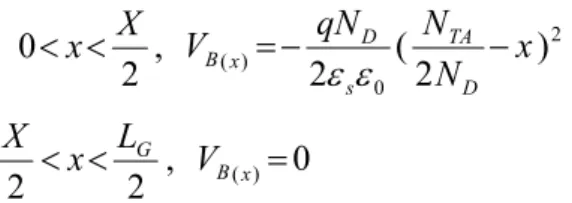
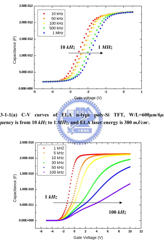
To confer the relation between the size of device and the capac cteristic of the poly-Si TFT, we measure the poly-Si TFTs with various channel length and LDD length. We observe that the measured C-V curve is shifted as the frequency increases in Fig.3-1-1(a) for the TFTs with small channel length, and the frequency dispersion phenomenon appears in depletion region as the frequency increases in fig.3-1-1(b) for the TFTs with large channel length. These devices in Fig.3-1-1 are ELA n-type poly-Si TFT, which channel width is 600µm and ELA laser energy is 380 mJ/cm2. In Fig.3-1-1(a), the curves are shifted toward the positive gate
voltage as the measured frequency increases from 10 kHz to 1 MHz, and the difference of the gate voltage is 0.7V. In the turn-off region and the turn-on region, the values of capacitance dose not change as the measured frequency increased. Capacitances in these two regions are independent with the measured frequency. In Fig.3-1-1(b), the curves appear the frequency dispersion phenomenon as the measured frequency increases from 1 kHz to 100 kHz. The measured frequency increase from 1 kHz to 10 kHz, and the curve is shifted toward the positive gate voltage. As the
measured frequency increases above 10 kHz, the values of capacitance start to decrease in the depletion region and the turn-on region. In the turn-off region, the value of capacitance dose not change as same as Fig.3-1-1(a). Capacitance in the turn-off region is independent with the measured frequency, and in the depletion region and the turn-on region are depend on the measured frequency. Compare to these two figures, the frequency dispersion is observed easily for the device with large channel length, and the curves starts to disperse at low measured frequency.
Fig.3-1-2 shows the C-V curves of n-type poly-Si TFT with various channel lengt
m. The turn- capacitance gr
h. The channel width of these devices is 600μm, and the measured frequency is 10 kHz. The value of capacitance in the turn-off region dose not change as the measured frequency increases, but that in the depletion and the turn-on region are increase as the measured frequency increases. In the turn-on region, the value of capacitance increased from 1.36×10⁻¹² F to 1.02×10⁻¹¹F with channel length
increasing from 4 μm to 30 μ on ows with the channel
length. In the previous studies, B. J. SHEU addressed a simple capacitance method for determining the channel length of devices [3.1]. The capacitance method is based on the linear relationship between the intrinsic gate capacitance and the effective channel length. In this method, the intrinsic gate capacitance can be expressed as
) (L L W t C ox ox= −Δ . ox ε
To extract the value of capacitance in the turn-on region, the plot of capacitance versus channel length for poly-Si TFTs is shown in Fig.3-1-3. This curve is a straight line. The intercept of the straight line at the abscissa gives ΔL=0.24μm. The
correlation coefficient for the straight line is better than 0.9998. U 0μm
and the slope in Fig.3-1-3, gate-oxide thickness is determined to be 60.7 nm. This line is almost through the origin. This analytical result proves that the measured value of capacitance is the oxide capacitance of devices in turn-on region.
Fig.3-1-4 shows the C-V curves of n-type poly-Si TFT with v
sing W = 60
arious LDD length.
influence t
n process, GI-clean step
the film with
The channel width (W) is 600 μm, the channel length (L) is 6 μm and the measured frequency is 10 kHz. The values of capacitance are not variable with LDD length increasing from 0.25 μm to 3.00 μm in the turn-off region, the depletion region, and the turn-on region. To extract the value of capacitance in turn-on region, the plot of capacitance versus LDD length for poly-Si TFTs is shown in Fig.3-1-5. This curve is a horizontal straight line, and the values of capacitance are almost the same,
F
12
10
2× − . This analytical result proves that the value of LDD length dose not
he measured value of capacitance.
3-1-2 Poly-Si TFTs with the fabricatio
Observing the measured result of capacitance can describe the change of
or without the fabrication process, GI-clean. These characteristic of device in Fig.3-1-6(a) is about p-type poly-Si TFT and in Fig.3-1-6(b) is about n-type poly-Si TFT. The W/L of the poly-Si TFT is 600μm/6μm, and the measured frequency is from 10 kHz to 1 MHz. The red curves stand for the device with doing GE-clean step, and the blue curves stand for the device without doing GI-clean step. This fabrication step, GI-clean, is to clean the surface of poly-Si layer before depositing the dielectric oxide layer on the poly-Si layer. In previous studies of C–V measurements [3.2], the fixed charges in the gate oxide of TFTs are not affected by a small applied signal, whereas the trap states in the band-gap respond to the applied frequency. If the C–V curve of the TFTs was slightly stretched out with increasing frequency, which may be attributed to an increase of the interface trap states. If the C–V curve of the TFTs was significantly shifted with increasing frequency, which may be attributed to an increase of trap states at the grain boundary. In these figures, the red curves are shifted toward the negative gate voltage, 3 V about p-type TFT and 4 V about n-type TFT. There is no stretched phenomenon in comparing the red curves to the blue curves. This analytical result proves that the flat-band of both type devices shift to negative side after GI-clean which indicates that GI-clean only increases positive trap states.
3-1-3 C-V measurement with various osc level
al gate voltage, and the osc C-V curve is measured by DC signal added AC sign
level is the height of the step gate voltage. With various osc level, the measured range of the gate voltage are different. With large osc level, the measured range is large, and the measured result of the capacitance is a comprehensive result of the poly-Si film. With small osc level, the measured range is small, and the measured result of the capacitance is a detailed result of the poly-Si film. Fig.3-1-7 shows the C-V curves of n-type poly-Si TFT with various osc level. The W/L of the poly-Si TFT is 600μm/6μm, LDD Length is 0.75 μm, and the measured frequency is 10 kHz. The range of osc level is from 0.1 V to 1.0 V. In the turn-off region or the turn-on region, the value of capacitance does not change with various osc level. In depletion region, the variation of capacitance is obviously different with various osc level. The red curve is measured by osc level 0.1V, and it increases more sharp as the gate voltage increases. As increasing the osc level, the curve becomes to increase gradually slowly. By osc level 1.0V, the curve is blue, and it increases most slowly as the gate voltage increased. The curves with various osc level are crossed in the depletion region, and this phenomenon shows in this figure. At small gate voltage of the depletion region, the value of measured capacitance at 1.0 V osc level is larger than at 0.1 V osc1evel. As the gate voltage increasing, the curves of capacitance measuring at various osc level
come closer and closer. Then, they approach the same value at certain gate voltage. At large gate voltage of the depletion region, the value of measured capacitance at 1.0 V osc level is smaller than at 0.1V osc1evel.
Fig.3-1-8 shows the schematic of the moving Fermi level on the Electron density of state-energy curve. The square wave represents the AC signal gate voltage. The large amplitude of square wave stands for the large osc level, and the small amplitude of square wave stands for the small osc level. At small gate voltage of the depletion region, in Fig.3-1-8(a), the Fermi level is located at deep state. The low levels of the small and the large osc level are both near the states below the Fermi level, but the high level of the large osc level is more near the states above the Fermi level than that of the small osc. level. The high level of the osc level dominates at small gate voltage of the depletion region, and the large osc level can measure much more. The value of measured capacitance by using the large osc level is larger than that by using the small osc level. At the large gate voltage of the depletion region, in Fig.3-1-8(b), the Fermi level is located at tail state. The high levels of the small and the large osc level are both near the states above the Fermi level, but the low level of the small osc level is more near the states below the Fermi level than that of large osc. level. The low level of the osc level dominates at large gate voltage, and the small osc level can measure much more. The value of measured capacitance by using the small osc level
is larger than that by using the large osc level. Using this description can explain the phenomenon in Fig.3-1-7.
3-2 The analysis of the C-f curve
ser energy
f the poly-Si film and the capa
i TFT with various eximer laser energ
3-2-1 Poly-Si TFTs with various la
To confer the relation between the grain size o
citance characteristic of the poly-Si TFT, we measure the poly-Si TFTs with various grain sizes. Fig.3-2-1 is the C-V curves of ELA n-type poly-Si TFT with various ELA laser energy densities. The W/L of these devices is 600µm/6µm, and the measured frequency is from 10 kHz to 1 MHz. The ELA laser energy densities of Fig.3-2-1(a), Fig.3-2-1(b), and Fig.3-2-1(c) are 380 mJ/cm2, 360 mJ/cm2, and 340
mJ/cm2, respectively. The device performance is shown in these three figures. The
shifted phenomenon of poly-Si TFT as the measured frequency increased is the most
serious about the ELA poly-Si TFTs with 340 mJ/cm2 laser energy density. The
excellent performance is the ELA poly-Si TFTs with 380 mJ/cm2 laser energy density.
The frequency dispersion phenomenon in the depletion region becomes more seriously which is discussed in the previous studies.
Fig.3-2-2 shows the C-f curves of p-type poly-S
y densities. The W/L of the poly-Si TFT is 600μm/6μm, and the measured frequency is from 10 kHz to 1 MHz. Table.1 lists the relationship between the laser
energy density and the average grain size. The poly-Si film with different laser energy density, the grain size of the poly-Si film is different. The laser energy is higher, the grain size will grow larger. In this figure, the red, green, and blue curves are the C-f characteristic of the ELA poly-Si TFTs with 380 mJ/cm2, 360 mJ/cm2, and 340 mJ/cm2
laser energy density, respectively. The red curve is like a sloping straight line, but the other two curves decay seriously, especially the blue curve. More pronounced frequency dispersion is observed in the characteristic of the device with smaller grain size.
3-2-2 A new simulation method for C-f curve
s of devices. The device in Fig.3-2-3 shows the C-f curves for various kind
Fig.3-2-3(a) is α-Si MIS, and the W/L of this device is 500μm/1000μm. Another device in Fig.3-2-3(b) is α-Si TFT, and the W/L of this device is 600μm/4.5μm. The other device in Fig.3-2-3(c) is poly-Si TFT with 380mJ/cm2 laser energy density, and
the device of W/L is 600μm/6μm. In Fig.3-2-3(a) and Fig.3-2-3(b), the C-f curves decay seriously as frequency increases. This similar phenomenon in Fig.3-2-2 is the green and blue curves. In Fig.3-2-3(c), the c-f curves are like sloping straight line as like the red curve in Fig.3-2-2. To compare Fig.3-2-2 and Fig.3-2-3, the speed of the C-f curve decay is due to the size of the grain. When the grain is small, the C-f curve decays fast, like the green and blue curve in Fig.3-2-2. Otherwise, the grain is large,
and the C-f curve decays slowly, like the red curve in Fig.3-2-2.
In Fig.3-2-4, the measured curves are simulated by using RPI model. This device is ELA n-type poly-Si TFT with 380mJ/cm2 laser energy density. The red curves are
simulated by using 1 ) ( 2 2+ = − sx sx sx SD G C r C C ω (10) and ] ) ( exp[ 2 1 2 1 2 ' T c th GS ox SD G sx V V V LW C C C η − − + × = = − (11)
, these two equations of RPI model, and the blue curves are measured. These curves
ulation of C-f is considered the Seto’s model, and the simulated steps are s
are not similar. The red curve decays suddenly at high frequency, but the blue curve is a sloping straight line to decay when the measured frequency increases. From this analytical result, the RPI model is not appropriate for the poly-Si TFTs with larger grain.
A new sim
hown in Fig.3-2-5. First, to calculate the energy barrier of grain is used by Seto’s model. In the case, ND<ND* : X =LG, the potential variation in the crystallite is
expressed by the following: )2
2 ( 2 x L qND G− − = ε ε In the other case,
0 ) ( V s x B G TA D D N X N > * : = f the potentia L N
, the expressions o l in the two
s follows: regions are shown a
2 0<x<X , 2 0 ) ( 2 (2N x) N qN V D TA s D x B =− ε ε − 2 2 G L x X < < , VB(x)=0
Fig.3-2-6 shows the curve of the energy band with various gate voltages. Second, this numerical simulation is used the transient carrier emission from deep level traps in poly-Si TFTs. en is the emission rate [3.3][3.4], defined by
exp( ) kT E E n e F i i n n n − =γσ ν . (12)
Using Eq.(12) and Fig.3-2-6, this simulation is putting the value of the energy band into Eq.(12) to get the relationship to the position of the emission rate, and compare the value of emission and the measured frequency.
Final, this step of new simulation is shown in Fig.3-2-7. The red region in this figure represents the activation region for a single grain. When the measured frequency is smaller the emission rate of all the carriers, all the carriers can be measured, in Fig.3-2-7(b). As the measured frequency increases, the partial carriers can not be measured due to their emission time are smaller then the measured frequency. The red activation region becomes small like Fig.3-2-7(c), Fig.3-2-7(d), and Fig.3-2-7(e). The ratio of the effective activation region (%) is equal to the activation region over the total region. Table.2 lists the parameter values of this new C-f simulation and this simulated result is shown in Fig.3-2-8. The curves for small grain size are calculated by using this new simulation in Fig.3-2-8(a) and for large
grain size are in Fig.3-2-8(b). The curves decay suddenly at high frequency in Fig.3-2-8(a), and this phenomenon is similar with the measured curve. The curves are like sloping straight line and decay slowly in Fig.3-2-8(a), and this phenomenon is also similar with the measured curves. Fig.3-2-9(a) is the measured curves and the simulated curves for small grain size, and Fig.3-2-9(b) is for large grain size. The simulation of the C-f curve is presented and shown to validate the experimental measurement. Finally, this new C-f simulation is appropriate for the poly-Si TFTs with larger grain.
Nomenclature
Cox Gate oxide capacitance [F/cm2]
Ea Activation energy [eV]
EF Fermi level [eV]
IDDrain current [A]
L Channel length [cm]
k Boltzmann constant [J/K]
NA Acceptor concentration [cm-3]
ND Induce charge concentration [cm-3]
N* Critical carrier concentration [cm-3] niIntrinsic concentration [cm-3]
q Elementary charge [1.6x10⁻¹⁹ coul.] T Absolute temperature [K]
tox Gate oxide thickness [cm]
tsi Silicon film thickness [cm]
VG Gate voltage [V]
V(x) Potential at grain-boundary depletion region [V]
W Channel width [cm]
x coordinate perpendicular to the channel [cm]
εox Oxide permittivity
εSi silicon permittivity
σn electron capture cross-section
Table
Table.1
The relationship between laser energy density and average grain size which is defined SEM images after secco etching.
Ec Ec-20 Ec-40 Laser energy density (mJ/cm2) 380 360 340
Table.2
The parameter values of the new C-f simulation for the W/L=600μm/6μm n-type poly-Si TFT with 1.25μm LDD length.
W [cm] 6.0×10⁻² ox C [F/cm2] 6.2×10⁻⁸ L [cm] 6.0×10⁻⁴ Si ε 3.9 Si t [cm] 6.0×10⁻⁶ ox ε 11.9 NTA [cm -3] 1.0×10¹² ε0 [F/cm] 8.85×10⁻¹⁴ ni [cm -3] 9.65×10⁹ K [J/K] 8.63×10⁻⁵ σn 1.0×10⁻¹⁶ T [K] 300 νn 2.3×10⁷ q [C] 1.6×10⁻¹⁹ LG [cm] 0.15 0.60 VG [V] ND [cm -3] γ VG [V] ND [cm -3] γ 0.8 5.16×10¹⁶ 50 0.2 1.29×10¹⁶ 0.003 1.0 6.45×10¹⁶ 50 0.8 5.16×10¹⁶ 0.003 2.0 1.10×10¹⁷ 50 2.0 1.10×10¹⁷ 0.003
Figure
-5 -4 -3 -2 -1 0 1 0.00E+000 5.00E-013 1.00E-012 1.50E-012 2.00E-012 2.50E-012 10 kHz 50 kHz 100 kHz 500 kHz 1 MHz Ca pacitan ce (F ) Gate voltage (V) 10 kHz 1 MHzFig.3-1-1(a) C-V curves of ELA n-type poly-Si TFT, W/L=600µm/6µm,
frequency is from 10 kHz to 1 MHz, and ELA laser energy is 380 mJ/cm2.
-6 -4 -2 0 2 4 6 8 10 12 0.00E+000 5.00E-011 1.00E-010 1.50E-010 2.00E-010 2.50E-010 1 kHZ 5 kHz 10 kHz 30 kHz 50 kHz 100 kHz Capacit ance (F) Gate Voltage (V) 1 kHz 100 kHz
Fig.3-1-1(b) C-V curves of ELA n-type poly-Si TFT, W/L=600µm/600µm,
-6 -4 -2 0 2 4 6 0.00E+000 2.00E-012 4.00E-012 6.00E-012 8.00E-012 1.00E-011 1.20E-011 b. n-type TFT LDD Length=0μm at 10k Hz a. W/L=600μm/4μm b. W/L=600μm/6μm c. W/L=600μm/10μm d. W/L=600μm/12μm e. W/L=600μm/15μm f. W/L=600μm/30μm Capacit an ce (F) Gate Voltage (V) a. c. d. e. f.
Fig.3-1-2 C-V curves of ELA n-type poly-Si TFT with various channel length at 10 kHz. Channel Length (μm) 0 5 10 15 20 25 30 Capa citance (F) 0 2x10-12 4x10-12 6x10-12 8x10-12 10x10-12 12x10-12 fitting line LDD Length 0μm
Fig.3-1-3 Capacitance-channel length curve of ELA n-type poly-Si TFT at large gate voltage.
-6 -4 -2 0 2 4 6 0.00E+000 2.00E-013 4.00E-013 6.00E-013 8.00E-013 1.00E-012 1.20E-012 1.40E-012 1.60E-012 1.80E-012 2.00E-012 2.20E-012 LDD Length=0.25μm LDD Length=0.50μm LDD Length=0.75μm LDD Length=1.25μm LDD Length=1.50μm LDD Length=1.75μm LDD Length=2.00μm Capacitance ( F ) Gate Voltage (V)
Fig.3-1-4 C-V curves of ELA n-type poly-Si TFT with various LDD length at 10
kHz. LDD Length (μm) 0.0 0.5 1.0 1.5 2.0 2.5 3.0 C apa cit an ce (F) 1.6x10⁻¹² 1.8x10⁻¹² 2.0x10⁻¹² 2.2x10⁻¹² 2.4x10⁻¹² W/L=600μm/6μm
Fig.3-1-5 Capacitance-LDD length curve of ELA n-type poly-Si TFT at large gate voltage.
p-type W/L=600μm/6μm Gate voltage (V) -12 -10 -8 -6 -4 -2 0 2 4 Capacitance (F) 0.0 500.0x10⁻¹⁵ 1.0x10⁻¹² 1.5x10⁻¹² 2.0x10⁻¹² 2.5x10⁻¹² With GI-Clean at 10K Hz With GI-Clean at 100K Hz With GI-Clean at 1M Hz Without GI-Clean at 10K Hz Without GI-Clean at 100K Hz Without GI-Clean at 1M Hz With GI-Clean Without GI-Clean
Fig.3-1-6(a) C-V curves of ELA p-type poly-Si TFT, W/L=600μm/6μm, and frequency from 10 kHz to 1 MHz. The red curves stand for the device with doing GI-clean process. The blue curves stand for the device without doing GI-clean process. n-type W/L=600μm/6μm Gate voltage (V) -10 -8 -6 -4 -2 0 2 4 6 8 Capa ci ta nc e (F) 0.0 500.0x10⁻¹⁵ 1.0x10⁻¹² 1.5x10⁻¹² 2.0x10⁻¹² 2.5x10⁻¹² With GI-Clean at 10K Hz With GI-Clean at 100K Hz With GI-Clean at 1M Hz Without GI-Clean at 10K Hz Without GI-Clean at 100K Hz Without GI-Clean at 1M Hz With GI-Clean Without GI-Clean
Fig.3-1-6(b) C-V curves of ELA n-type poly-Si TFT, W/L=600μm/6μm, LDD length=0.75μm, and frequency from 10 kHz to 1 MHz. The red curves stand for the device with doing GI-clean process. The blue curves stand for the device without doing GI-clean process.
-1.0 -0.8 -0.6 -0.4 -0.2 0.0 0.2 0.4 0.6 0.8 1.0 1.2 1.4 1.6 1.8 2.0 2.2 2.4 0.00E+000 5.00E-013 1.00E-012 1.50E-012 2.00E-012 2.50E-012 n-type TFT W/L=600um/6um LDD Length=0.75um at frequency=10k HZ osc level 0.1V osc level 0.2V osc level 0.5V osc level 0.8V osc level 1.0V Capacitan ce (F ) Gate Voltage (V)
Fig.3-1-7 C-V curves of ELA n-type poly-Si TFT with various osc level at 10 kHz.
Fig.3-1-8 The schematic of the moving Fermi level on the electron density of state-energy curve. (a) at small gate voltage (b) at large gate voltage
-1.5 -1.0 -0.5 0.0 0.5 1.0 1.5 2.0 0.00E+000 5.00E-013 1.00E-012 1.50E-012 2.00E-012 2.50E-012 3.00E-012 10 kHz 50 kHz 100 kHz 500 kHz 1 MHz C a pa ci ta nc e (F) Gate Voltage (V) (a) -1.5 -1.0 -0.5 0.0 0.5 1.0 1.5 2.0 0.00E+000 5.00E-013 1.00E-012 1.50E-012 2.00E-012 2.50E-012 3.00E-012 (b) 10k Hz 50k Hz 100k Hz 500k Hz 1M Hz C apa citance (F) Gate Voltage (V) -1.5 -1.0 -0.5 0.0 0.5 1.0 1.5 2.0 0.00E+000 5.00E-013 1.00E-012 1.50E-012 2.00E-012 2.50E-012 3.00E-012 (c) 10k Hz 50k Hz 100k Hz 500k Hz 1M Hz Cap a ci tance (F ) Gate Voltage (V)
Fig.3-2-1 C-V curves of ELA n-type poly-Si TFT, W/L=600µm/6µm, frequency is
and (c) 340 mJ/cm2. n-type TFTs W/L=600μm/6μm LDD length=0.75μm at VG=0.6V Frequency (Hz) 10x103 100x103 1x10⁶ C a pacitance (F) 0.0 500.0x10⁻¹⁵ 1.0x10⁻¹² 1.5x10⁻¹² 2.0x10⁻¹² 2.5x10⁻¹² 380 mJ/cm2 Grain Size=0.60um 360 mJ/cm2 Grain Size=0.25um 340 mJ/cm2 Grain Size=0.15um
Fig.3-2-2 C-f curves of ELA p-type poly-Si TFT, W/L=600μm/6μm, with various eximer laser energy.
10000 100000 1000000 4.00E-013 6.00E-013 8.00E-013 1.00E-012 1.20E-012 1.40E-012 1.60E-012 1.80E-012 2.00E-012 VG = 0.00V VG = 1.00V VG = 1.25V VG = 1.50V VG = 1.75V VG = 2.25V VG = 2.75V VG = 4.00V VG = 7.00V VG = 10.00V Ca paci tance ( F ) Frequency (Hz) V G = 10.00V V G = 0.00V 10000 100000 1000000 4.00E-013 6.00E-013 8.00E-013 1.00E-012 1.20E-012 1.40E-012 1.60E-012 1.80E-012 2.00E-012 Vg=0.0V Vg=0.5V Vg=0.75V Vg=1.0V Vg=1.25V Vg=1.5V Vg=1.75V Vg=2.0V C apaci tance ( F ) Frequency (Hz) V G = 2.0V VG = 0.0V 10000 100000 1000000 6.00E-011 6.20E-011 6.40E-011 6.60E-011 6.80E-011 7.00E-011 7.20E-011 7.40E-011 7.60E-011 7.80E-011 8.00E-011 8.20E-011 8.40E-011 8.60E-011 VG= -5.0V VG= -4.0V VG= -2.5V VG= -1.0V VG= 0.0V VG= 0.5V VG= 1.0V VG= 2.5V VG= 5.0V VG= 7.5V VG= 10.0V VG= 12.5V VG= 15.0V Ca paci tance ( F ) Frequency (Hz) V G = 15.0V VG = -5.0V (a) (c) (b)
Fig.3-2-3 C-f curves of various kind of TFT. (a) α-Si MIS, W/L=500μm/1000μm. (b) α-Si TFT, W/L=600μm/4.5μm. (c) poly-Si TFT, W/L=600μm/6μm, with laser
energy density=380mJ/cm2. W/L=600μm/6μm Frequency (Hz) 10x103 100x103 1x10⁶ Capa citance (F) 600.0x10⁻¹⁵ 800.0x10⁻¹⁵ 1.0x10⁻¹² 1.2x10⁻¹² 1.4x10⁻¹² 1.6x10⁻¹² 1.8x10⁻¹² 2.0x10⁻¹² 2.2x10⁻¹² a. Simulation at VG=1.0V b. Simulation at VG=1.5V c. Simulation at VG=2.0V a'. Measurement at VG=1.0V b'. Measurement at VG=1.5V c'. Measurement at VG=2.0V a'. b'. c'. a. b. c.
Fig.3-2-4 The curves are simulated by using the RPI model. The device is ELA n-type poly-Si TFT with laser energy density, 380mJ/cm2.
x (cm) -100x10-6 -80x10-6 -60x10-6 -40x10-6 -20x10-6 0 20x10-6 40x10-6 60x10-6 80x10-6 100x10-6 E ( e V) 0.0 0.2 0.4 0.6 0.8 1.0 VG = 0.10V VG = 0.20V
(a) The case of ND < ND*
x (cm) -100x10-6 -80x10-6 -60x10-6 -40x10-6 -20x10-6 0 20x10-6 40x10-6 60x10-6 80x10-6 100x10-6 E (eV ) 0.0 0.2 0.4 0.6 0.8 1.0 VG = 0.7V VG = 1.0V VG = 2.0V (b) The case of ND > ND*
Fig.3-2-6 The curve of the energy band with various gate voltages for grain size of 600 nm.
Grain Size = 0.15 μm Frequency (Hz) 10x103 100x103 1x10⁶ % 0.0 0.2 0.4 0.6 0.8 1.0 a. VG = 0.8 V Grain Size = 0.15μm b. VG = 1.0 V Grain Size = 0.15μm c. VG = 2.0 V Grain Size = 0.15μm a. b. c.
Fig.3-2-8(a) The curves are calculated by using this new simulation for small grain. Grain Size 0.60μm Frequency (Hz) 10x103 100x103 1x10⁶ % 0.0 0.2 0.4 0.6 0.8 1.0 a. VG = 0.2 V Grain size = 0.60μm b. VG = 0.8 V Grain size = 0.60μm c. VG = 2.0 V Grain size = 0.60μm a. b. c.
Fig.3-2-8(b) The curves are calculated by using this new simulation for large grain.
Frequency (Hz) 10x103 100x103 1x10⁶ % 0.0 0.2 0.4 0.6 0.8 1.0 Simulation at VG = 0.8 V Simulation at VG = 1.0 V Simulation at VG = 2.0 V Mesure at VG = 0.8 V Mesure at VG = 1.0 V Mesure at VG = 2.0 V VG = 2.0V VG = 1.0V VG = 0.8V
Fig.3-2-9(a) The measured curves and the simulated curves for small grain size.
Frequency (Hz) 10x103 100x103 1x10⁶ % 0.0 0.2 0.4 0.6 0.8 1.0 Simulation at VG = 0.2 V Simulation at VG = 0.8 V Simulation at VG = 2.0 V Measure at VG = 0.2 V Measure at VG = 0.8 V Measure at VG = 2.0 V VG = 2.0V VG = 0.8V VG = 0.2V
Reference
[3.1] B. J. SHEU, student member, and P. K. KO, member, “A Capacitance Method to Determine Channel Lengths for Conventional and LDD MOSFET’s”, Electron Device Letters, Vol.EDL-5, No.11, November 1984
[3.2] Kook Chul Moon, Jae-Hoon Lee, and Min-Koo Han, “The Study of Hot-Carrier Stress on Poly-Si TFT Employing C–V Measurement”, IEEE Transactions on Electron on Devices, Vol.52, No.4, April 2005
[3.3] G.. A. Armstrong, J.R. Ayres, and S. D. Brotherton, “Numerical Simulation of Transient Emission from Deep Level Traps in Polysilicon Thin Film Transistors”, Solid-State Electronics, Vol.41, No.6, pp.835-844, January 1997
[3.4] J. G Simmons and L. S. Wei, , “Theory of transient emission current in MOS devices and the direct determination interface trap parameters”, Solid-State Electronics, Vol.17, Issue 2, pp.117-124, February, 1974
Chapter 4
Conclusion
In this thesis, the poly-Si TFTs were fabricated by excimer laser annealing recrystallization technology and the measurement work was done for the poly-Si TFTs of the same channel, various channel length and LDD length at AC small gate bias under the same environment temperature.
We studied new simulation of capacitance-frequency measurement and the classical characteristic of poly-Si TFTs. We assure the measured capacitance in turn-on region is only the oxide capacitance by varying the scale of devices. The change fabrication of devices will influence the characteristic of devices. Measuring C-V and observing the variation of characteristic curve can identify how the devices make changes after doing the varied fabrication. By this method, we can derive the better fabrication process for device.
In our experiment, we measure C-V curve by using various osc level. The value of osc level influences the measurement. Using the large value, the height of AC step signal is large, and the sweep range of gate voltage is large. We can obtain the rough of the characteristic of device in this measured result. Using the small value, we can obtain more details of the devices.
In the past, the grain size if the poly-Si film is small. The characteristic of this device can simulate by using RPI model appropriately. When the poly-Si TFT technology is improving, the grain size becomes much larger. The pronounced frequency dispersion of poly-Si TFT is not serious, and the RPI model or the pre-studies is not appropriate for the poly-Si TFTs when the grain size of device is larger. In our study, we use a new simulated method for the poly-Si TFTs with large grain or small grain. There are grain boundaries in the poly-Si material, and these grain boundaries act as energy barriers that the carriers have to come. The grain boundaries are crucial. We consider the emission time of the carrier for poly-Si TFTs. In this analysis result, the simulation and the measurement are appropriate for the characteristic of this device.