國 立 交 通 大 學
電子工程學系 電子研究所碩士班
碩 士 論 文
具可調整預先增強器之
6Gbps 串列連結傳輸器
A 6Gbps Serial Link Transmitter
with Tunable Pre-emphasis
研 究 生 :朱昌敏
指導教授:周世傑 教授
A 6Gbps Serial Link Transmitter
with Tunable Pre-emphasis
研 究 生:朱 昌 敏
Student : Chang-Min Chu
指導教授:周 世 傑 教授
Advisor :Pro. Shyh-Jye Jou
國立交通大學
電子工程學系 電子研究所碩士班
碩士論文
A thesis
Submitted to Institute of Electronics
College of Electrical Engineering and Computer Science
National Chiao Tung University
In Paritial Fulfillment of the Requirements
for the Degree of
Master of Science
In
Electronic Engineering
July 2006
一直以來,個人電腦平臺的硬碟裝置,向來都是平行化 ATA 的介面規格,而 隨著傳輸速率的提升,在高達 1.5Gbits/sec 下,以現有的平行化架構,難以再 將頻寬提升。因此串列式 ATA 的技術規格因應而生,而第三代串列式 ATA 之應用 將於 2007 年普及,到時,硬碟裝置的傳輸速度將可到達 6Gbits/sec。 本論文中,我們主要完成高速串列連結之資料傳輸器並且建構可調變式信號 預先加強器電路於其中,以符合串列式 ATA 的規格。首先,針對串列式 ATA 規 格以及高速傳輸器做一個概略的介紹與導讀。接下來,詳述傳輸器的電路架構以 及設計理念,並且針對具有自我調整的預先加強器電路做介紹,最後,列出晶片 的量測結果。 整體電路為採用 TSMC 0.18um 1P6M CMOS 製程技術予已實現。此傳輸器在 經過十公尺的纜線傳輸情況下仍可以達到傳輸速率 6Gbps。且在電壓電源為 1.8V 下,總消耗功率為小於 130mW。
For a long period of time, the industrial I/O standard interfaces for
connecting storage device inside personal computers is Parallel Advanced
Technology Attachment (PATA). However, due to the challenges in increasing the
speed of ATA specification, a shift in design strategy is required. The new
approach is Serial ATA specification. The application of SATA III will be
available to all in 2007. At that time, the data rate of storage device such as hard
discs will operated at 6Gbps.
In this thesis, we implement a high speed serial link data transmitter with
tunable pre-emphasis to fit with serial ATA specification. First, we introduce the
serial link and serial ATA specification. Then, we describe the transmitter circuit
and design issue. We also introduce the concept of the tunable pre-emphasis.
Finally, the measurement results are showed and listed.
The whole circuit is implemented by TSMC 0.18um 1P6M CMOS
technology. The circuit can transmit data at 6Gbps data rate with 10m cable
length. The supply voltage is 1.8v and the total power consumption is less than
兩年來的碩士生涯,隨著論文的完成而接近了尾聲。從晶片的設計,模擬, 下線到量測,感謝一路指導我的周世傑教授,我永遠忘不了第一次與您見面時, 您在麥當勞喝著可樂且與我開心暢談的時刻。謝謝老師帶領我進入電機這門領 域,教導我們專業知識以及台風應答的的技巧。 感謝指導我們的林志憲學長,沒有你的細心的 "叮嚀"及教導,也就沒有 今天的成果,希望能早日喝到學長的喜酒。且感謝在量測實驗室的志龍學長及嘉 琳學姐,PCB 板與晶片沒有你們的協助,也不可能有完美的量測結果,最後在 803 的日子,過得很開心。 另外感謝我的好伙伴,誌華。還記得當時趕下線,兩個人熬到半夜在 debug, 截止前奔跑到 CIC 的窘境。當時每天努力的打拼,如今總算有了一點小小的成 果。實驗室的庭楨大大,一心大大,已畢業的套哥,MOMO 學姐,小胖,小肥, 亦瑋,琪耀,志雄,阿賢,五位帥氣的交大學弟,阿樸,俊誼,SPICE,俊男, 國光。由於你們的陪伴,不管是在實驗室打嘴砲,晚上電影院,實驗室出遊,最 後 VLSI/CAD 的泛舟和溯溪,都讓小朱過了很開心又充實的兩年碩士生活。還有 感謝陪伴我兩年的大學同學兼室友,科學人,子倫,css,小趙,八組組,炮哥, 一起逛街,一起運動,一起出遊,因為有你們,豐富了我的碩士人生。 最後更要感謝我的父母,謝謝你們一路栽培,你們辛苦了。孩兒終於拿到碩 士學位,這份榮譽也是屬於你們的。 2006.08.15 朱昌敏
Content
Chapter 1 Introduction...1
1.1 Introduction of High-Speed Serial Link ...1
1.2 Motivation and Goals...3
1.3 Thesis Organization ...4
Chapter 2 Serial ATA ...5
2.1 Introduction to Serial ATA Specifications...5
2.2 Physical Layer of Serial ATA...7
2.3 Transmitter Driver of Serial ATA...9
2.3.1 Low Voltage Differential Signaling (LVDS)...9
2.3.2 Current Mode Logic (CML) ... 11
2.3.3 The Comparison between LVDS and CML...12
Chapter 3 Architecture of Serial ATA Transmitter ...17
3.1 Introduction...17
3.2 The Architecture of Serial ATA Transmitter ...18
3.3 Functional Blocks of Transmitter...19
3.3.1 PRBS and K28.5 ...19
3.3.2 AMUX and BMUX...20
3.3.3 Synchronizer ...21
3.3.4 CMUX...22
3.4 Pre-emphasis ...23
3.4.1 Overview...24
3.4.2 Methodology and Design...28
3.4.3 Architecture and Comparison ...32
3.5 Summary ...35
Chapter 4 Serial ATA Transmitter Circuit Design ...36
4.1 Introduction...36
4.2 Transmitter Design Issues...37
4.3 Circuit Design and Simulation Results ...38
4.3.1 Input Data...39
4.3.2 Synchronizer ...41
4.3.3 PISO...42
4.3.4 Pre-emphasis and Data Driver ...44
4.5 Summary ...53
Chapter 5 Experimental Results ...54
5.1 Layout and Experimental Setup...54
5.2 Print Circuit Board Setup...57
5.3 Experimental Results ...58
Chapter 6 Conclusions...64
List of Figures
Fig. 2.1 Serial ATA Communications Layer Model...6
Fig. 2.2 Physical Plant Overall Block Diagram [4] ...7
Fig. 2.3 (a) CML Structure (b) LVDS Structure [4]...10
Fig. 2.4 LVDS Driver and Receiver Structure ... 11
Fig. 2.5 CML Driver and Receiver Structure...12
Fig. 2.6 Driver architecture (a)LVDS (b)CML ...13
Fig. 2.7 The transceiver structure (a) LVDS structure (b) CML structure...14
Fig. 3.1Tranceiver architecture ...18
Fig. 3.2 Transmitter architecture...19
Fig. 3.3 Timing Diagram of the transmitter ...21
Fig. 3.4 Synchronization function block...22
Fig. 3.5 PISO timing diagram ...23
Fig. 3.6 PISO architecture...23
Fig. 3.7 (a) The input signal in the transmitter (b) The output signal in the receiver ..25
Fig. 3.8 Signaling waveform (a) without pre-emphasis (b) with pre-emphasis...25
Fig. 3.9 Block diagram of a pre-shaping parallel transmitter for MIT group [11] ...27
Fig. 3.10 Block diagram of a pre-shaping parallel transmitter for Stanford group [12] ...28
Fig. 3.11 Two kinds of pre-emphasis ...29
Fig. 3.12 Signaling in TX RX and ISI cancellation...30
Fig. 3.13 Frequency response of the transmission with pre-emphasis ...30
Fig. 3.14 Total frequency response without pre-emphasis...32
Fig. 3.15 Frequency response of one bit delay time FIR for (a) 5m (b) 10m cable...32
Fig. 3.16 CML driver and pre-emphasis driver ...33
Fig. 3.17 The pre-shaped signal in the transmitter with different data rate ...34
Fig. 4.1 Transceiver architecture...37
Fig. 4.2 Frequency response of PAD ...38
Fig. 4.3 Frequency response of 5m cable ...38
Fig. 4.4 10-bit PRBS encoder ...39
Fig. 4.5 Simulation waveform with 10-bit PRBS encoder ...40
Fig. 4.6 Simulation waveform with K28.5 input pattern ...40
Fig. 4.7 Simulation waveform with K28.5 and PRBS input patterns ...41
Fig. 4.8 5-bits data synchronizer...42
Fig. 4.10 Logic drive block of PISO...43
Fig. 4.11 Charge sharing effect [14] (a) without charge compensation (b)with charge compensation ...44
Fig. 4.12 Pre-emphasis and data driver architecture...45
Fig. 4.13 FDT Pre-emphasis detail circuit (a) Tunable CML buffer (b) CML buffer..46
Fig. 4.14 CML MUX and CML driver circuit (a) CML MUX (b) CML Driver ...47
Fig. 4.15 The simple diagram of TX and RX ...47
Fig. 4.16 The simulation results of Vin+/- and CML+/- node ...48
Fig. 4.17 The simulation results of CML and ECML node (a) FDT (b) OBT...49
Fig. 4.18 RX-eye with fixed and 1 bit delay time pre-emphasis under 6Gbps...50
Fig. 4.19 RX-eye with fixed and 1 bit delay time pre-emphasis under 3Gbps...50
Fig. 4.20 RX-eye with modified half bit delay time pre-emphasis under 3Gbps ...51
Fig. 4.21 The eye diagram of receiver (cable length=10m)...52
Fig. 5.1 Transmitter layout...55
Fig. 5.2 The experimental setup for the transmitter...56
Fig. 5.3 Transmitter chip micrograph ...57
Fig. 5.4 The PCB for testing ...58
Fig. 5.5 Jitter histograms of the PLL at 100MHz ...59
Fig. 5.6 Timing diagram of the PLL at 100MHz ...59
Fig. 5.7 Measurement result of K28.5 pattern ...60
Fig. 5.8 Simulation result of K28.5 pattern ...60
Fig. 5.9 PRBS waveform without pre-emphasis in 6Gbps ...61
Fig. 5.10 PRBS waveform with pre-emphasis in 6Gbps ...61
Fig. 5.11 TX output Eye diagram of PRBS pattern without pre-emphasis at 6Gbps ..62
Fig. 5.12 TX output Eye diagram of PRBS pattern with pre-emphasis at 6Gbps ...62
List of Tables
Table 1.1 Industrial standard for high speed serial link ...2
Table 1.2 Parallel ATA vs. Serial ATA ...3
Table 1.3 Generation for Serial ATA [4] ...3
Table 2.1 Signals in Control Block ...8
Table 2.2 The size of the two drivers ...15
Table 2.3 The power comparison of the two drivers...15
Table 4.1 Pre-emphasis performance comparison (Cable length =5M)...50
Table 4.2 Simulation results summary of the transmitter ...52
Table 4.3 Comparisons of the performance between our design and other papers...53
Table 5.1 Chip version ...56
Chapter 1
Introduction
1.1 Introduction of High-Speed Serial Link
As the CPU speed reaches 3GHz and beyond, the I/O performance has increasingly become the bottleneck of the overall system performance. The I/O peripheral is increasing speed from hundreds of Mbps to Gbps for the next generation. More and more high speed serial link industrial standard are set up either over short distance in copper cable or longer distance in fiber. (See Table 1.1) The common characteristics of the standard are differential signals with low swing and current mode transceiver with low power.
Advanced Technology Attachment (ATA) is one of the industrial I/O standard interface for connecting storage devices inside personal computers. Parallel ATA (P-ATA) is the primary internal storage interconnect for the desktop in early stages, which connecting the host system to peripherals such as hard drivers, optical drivers,
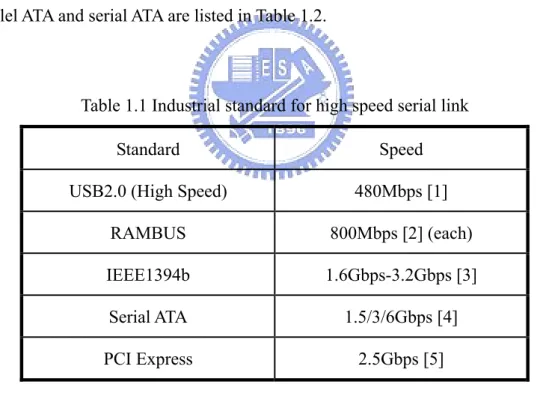
and removable magnetic media devices. However, due to the challenges in increasing the speed of the ATA specification, a shift in design strategy is required. The new approach is Serial ATA [4]. It addresses this need by making the transition to a high-speed serial bus. Comparing with parallel ATA interface, Serial ATA deals with some drawbacks and provides a scalable platform to support several generations of future storage devices. Serial ATA is an improved solution that is compatible with today's software and workable with the new architecture without modification. It provides for systems which are easier to design, with cables that are simple to route and install, smaller cable connectors, improve silicon design, and lower voltages which alleviate current design requirements in Parallel ATA. The comparison of parallel ATA and serial ATA are listed in Table 1.2.
Table 1.1 Industrial standard for high speed serial link
Standard Speed USB2.0 (High Speed) 480Mbps [1]
RAMBUS 800Mbps [2] (each)
IEEE1394b 1.6Gbps-3.2Gbps [3] Serial ATA 1.5/3/6Gbps [4]
Table 1.2 Parallel ATA vs. Serial ATA
P-ATA S-ATA Maximum Speed 1.33Gbps > 1.5Gbps
Cable Length 18 Inches 1Meter (About 40 inches) Cable Pins 40 7
Chip Core Voltage 5V 250mV Hot Swappable No Yes
1.2 Motivation and Goals
Serial ATA [4] is the new internal storage interconnect standard designed to replace parallel ATA technology. This architecture overcomes the electrical constraints that are difficulty to enhance 1.5G speed for the classic parallel ATA bus. Serial ATA I was introduced at 1.5Gbits/sec, with a roadmap planned to 6Gbits/sec (Table 1.3). It supporting up to 10 years of storage evolution based on historical trends [6].
The goal of this research is to design a 6Gbps S-ATA transmitter. Based on the S-ATA II specification, we try to design a S-ATA III transmitter. The target technology is TSMC 1P6M 0.18um 1.8V CMOS process.
1.3 Thesis Organization
The thesis organization is described as follows:
Chapter 2 introduces the specifications of Serial ATA, including the physical plant block diagram, signal specifications and transmitter examples. We also compare the two type drivers which are CML and LVDS in this chapter.
Chapter 3 shows the proposed transmitter architecture and explains the pre-emphasis method to overcome the bandwidth of the line as the length is increased.
Chapter 4 will discuss some detail circuit design methodology of the transmitter. Also, a novel pre-emphasis circuit is proposed. The implementation of functional block and simulation results of transmitter are also described in this chapter.
Chapter 5 shows the experimental results and introduces the measurement equipment we used to measure the chip. Some measurement results are also shown in this chapter.
Chapter 2
Serial ATA
2.1 Introduction to Serial ATA Specifications
Serial ATA (SATA) [4], an evolutionary high-performance interface for storage devices to replace the Parallel ATA, is used to connect ATA and ATAPI devices. Serial ATA has many advantages as following:
y Point to point connection topology ensures dedicated 1.5Gbits/sec to each device
y Thinner, longer cables for easier routing
y Fewer interface signals require less board space and allow for simpler routing
y Better connector design for easier installation and better device reliability y Hot-swap capability
There are four layers, Application, Transport, Link, and Physical layers in the Serial ATA architecture shows in Fig. 2.1. The Application layer is responsible for overall ATA command execution, including controlling Command Block Register accesses. The Transport layer is responsible for placing control information and data to be transferred between the host and device in a packet/frame, known as a Frame Information Structure (FIS). The Link layer is responsible for taking data from the constructed frames, encoding or decoding each byte using 8b/10b, and inserting control characters such that the 10-bit stream of data may be decoded correctly. The Physical layer is responsible for transmitting and receiving the encoded information as a serial data stream on the wire.
4 Application Layer 3 Transport Layer 2 Link Layer 1 Physical Layer Fig. 2.1 Serial ATA Communications Layer Model
The target services of physical layer in Serial ATA are listed below. For the transmitter end, the 10, 20, 40, or other width parallel input from the link layer are serialized for transmission. Then the transmitter delivers 1.5, 3 or 6Gbps differential NRZ serial stream data at specified voltage level with 100 Ohm matched termination through cable to receiver. For the receiver end, it receives differential NRZ serial stream with data rates of ± 350 ppm with +0/-500 ppm (due to spread spectrum profile)
from the nominal data rate. Then the receiver shall extract data and clock from the serial stream and de-serial the stream data. The transceiver can optionally support
power management modes and impedance calibration in the transceiver. Our research is emphasizing on the Physical layer to design a SATA transmitter. The more detail information about Physical are show in the next section.
2.2 Physical Layer of Serial ATA
The Serial ATA physical layer (PHY) uses low-voltage differential signaling to enable speeds from 1.5Gb/s to 6.0Gb/s. The PHY layer incorporates serializer/deserializer, provides out of band (OOB) signaling, and handles power–on sequencing and speed negotiation. Transmit Data is serialized from 10-bit characters, and Receive Data is deserialized to 10-bit characters. Device status feedback is provided to the link layer. The overall physical block diagram is shown in Fig. 2.2. We focus on the Transmitter end.
The DATAIN[0:n] from link layer and from 8b/10b coding are usually parallel data stream in order to increase the bandwidth of the link. There are also lots of alternative fixed control pattern sources from control block, mainly to provide the supporting circuitry that generates the patterns as needed to implement the ALIGN primitives activity defined in SATA specification [4]. The control block is a collection of logic circuitry that controls the overall functionality of physical plant circuitry (Table 2.1).
Table 2.1 Signals in Control Block PHYreset
This input signal causes the physical layer to initialize to a known state and start generating the COMRESET OOB signal across the interface.
PHYready
Signal indicating Physical has successfully established
communications. The Physical is maintaining synchronization with the incoming signal to its receiver and is transmitting a valid signal on its transmitter.
Slumber Causes the physical layer to transition to the Slumber power management state.
Partial Causes the physical layer to transition to the Partial power management state.
NearAFELB Causes the physical layer to loop back the serial data stream from its transmitter to its receiver.
FarAFELB Causes the physical to loop back the serial data stream from its receiver to its transmitter.
SpdSel Causes the control logic to automatically negotiate for a usable interface speed or sets a particular interface speed.
SpdMode Output signal that reflects the current interface speed setting. System Clock
This input is the clock source for much of the control circuit and is the basis from which the transmitting interface speed is
After that we need a Parallel In Serial Out (PISO) circuit before sending data to the analog front end. The PISO circuit can convert parallel digital bits into a serial analog signal stream with TX clock. Finally, the serial data in the analog front end is delivered by the high speed differential driver through channel to the receiver.
2.3 Transmitter Driver of Serial ATA
There are two transmitter examples from Serial ATA specification shown in Fig. 2.3. We can see both Current Mode Logic (CML) and Low Voltage Differential Signaling (LVDS) circuits can implement the SATA transmitter. The figure also indicates how the transition to and from the idle state can be implemented. When the signal of idle pin is high, it will cause the CML or LVDS input switch MOS to turn off. Therefore, there will be no data transition on the cable. The termination of the both structure are 100 ohm in order to match the cable equivalent termination. Following is the detail discussion of the two structures.
2.3.1 Low Voltage Differential Signaling (LVDS)
LVDS is a high-speed and low-power general purpose interface standard that solves the bottleneck problems while servicing a wide range of application areas. There are two industry standard specifications for LVDS, one is ANSI/TIZ/EIA-644 [7] and the other is IEEE 1596.3 SCI-LVDS [8]. They specify a little different output range, but the IEEE 1596.3 only addressed the high data rates and did not address the low power concern. ANSI/TIZ/EIA-644 is the more common standard. It specifies a differential output voltage swing in the interval 250 mV to 450 mV. LVDS basically
specifies circuits with 2.5V or 3.3V power supplies. If we want to implement this standard into TSMC 0.18um technology for our S-ATA data driver, we have to modify some rules.
(a)
(b)
Fig. 2.3 (a) CML Structure (b) LVDS Structure [4]
The LVDS output structure is shown in Fig. 2.4. The LVDS driver and receiver connected via differential impedance media. In order for the differential output to be terminated correctly, a 100 ohm resistor has to be connected between OUT+ and OUT- at the receiver and driver end. The driver consists of a current source which drives the differential pair lines. This current will run through the 100 ohm termination resistor, and the direction of this current will change every time the output shifts from “high” to “low” or the opposite according to the four MOS switch ( M1 -
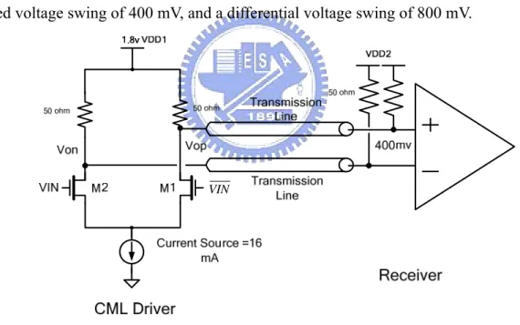
M4). The direction of the output current is controlled by letting one side of the differential output stage either sink or source current, while the other side of the differential output stage does the opposite (push-pull). Assuming that the current source in the LVDS output stage is 8 mA, this structure yields a single ended voltage swing of 400 mV, and a differential voltage swing of 800 mV.
Vop Von VIN VIN M2 M4 M1 M3 1.8v 100 ohm
Current Source =8mA
8mA 400mv Transmission Line Transmission Line LVDS Driver Receiver 100 ohm VIN VIN
Fig. 2.4 LVDS Driver and Receiver Structure
The LVDS input structure has the advantage of a wide input voltage range (0 volt – 1.8 volt), and a low differential input voltage threshold of 100 mV. The wide input voltage range combined with the low differential input voltage threshold, allows for a ± 1 volt difference in ground potential between the LVDS driver and the LVDS
receiver.
2.3.2 Current Mode Logic (CML)
Fig. 2.5 shows the CML structure [9][10]. It has the advantage of requiring without any external termination resistors. The termination resistors are an integrated
part of the input and output structure. The CML output stage consists of a differential pair, and the logic function is implemented by shifting the current between the two halves of the differential pair. Assume the current source is 16mA. When one of the differential outputs (OUT+ or OUT- ) is in ”low” state, 8 mA will be drawn from the power supply Vcco and 8 mA will be drawn from the power supply Vcci of the CML input stage to which the differential CML output is connected. The current is drawn equally from the two supplies because the input impedance of the CML input stage is 50 ohm, and thus equal to the resistor in the output stage. Assuming that the current source in the CML output stage is 16 mA, the single ended output “high” voltage is Vcc, and the single ended output “low” voltage is Vcc - 0.4 volt. This yields a single ended voltage swing of 400 mV, and a differential voltage swing of 800 mV.
VIN
Fig. 2.5 CML Driver and Receiver Structure
2.3.3 The Comparison between LVDS and CML
The Low Voltage Differential Signaling (LVDS) structure and the Current Mode Logic (CML) structure have been developed to provide the high-speed and low-power
interface application shown in Fig. 2.6. The target of our research is to design a 6Gbps transmitter for S-ATA III, and both of the structures can operated at high-speed. Therefore, power, area and switch sensitivity would be our major concern. We discuss these two structures under the same differential output swing condition by using 0.18um 1.8v CMOS process.
(a) (b) Fig. 2.6 Driver architecture (a)LVDS (b)CML
For LVDS architecture shown in Fig. 2.6(a), it has a 2R differential termination between transmitter and receiver. The signal-ended output voltages would be either Vocm+RI or Vocm-RI, and the differential swing is 2RI. For CML architecture shown in Fig. 2.6(b), it consists of an independent parallel termination R between transmitter and receiver, and current 2I is steered either in the left or right transistor. The single-ended output voltage would be either VDD or VDD-2RI, and the differential swing is equal to 2RI. So the power dissipation in CML driver is twice bigger than in LVDS driver. However, the data driver consists of driver and pre-driver. In order to meet LVDS standard, the size of the four input transistors shall be designed very large. Thus, the sizes of the pre-driver must also be increased to drive the PMOS and NMOS
input transistors. This will cause the total power of LVDS driver plus pre-driver much larger than that of CML.
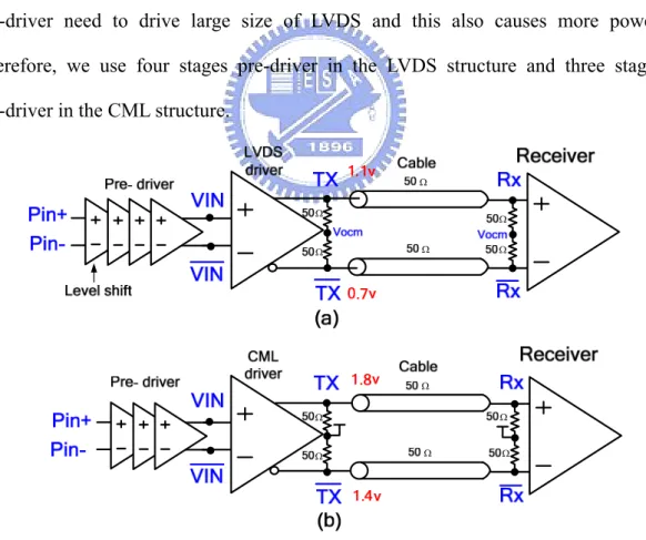
We use these two kinds of data driver to design our transmitter to fit with the SATA specification shown in Fig. 2.7. Here, we make the output differential swing in the TX node are both 700mV. Thus, the current of LVDS driver is half of CML and the power consumption of LVDS is less than CML. The size of LVDS and CML is listed in Table 2.2. From this table, we can find out that the size of LVDS is larger than CML. Moreover, the voltage swing of LVDS is in the central range, thus we need to use a level shift circuit to shift voltage level such that it can driver the LVDS in the correct function. This will cause more power in the pre-driver stage. Besides, pre-driver need to drive large size of LVDS and this also causes more power. Therefore, we use four stages pre-driver in the LVDS structure and three stages pre-driver in the CML structure.
Ω Ω Ω Ω Ω Ω Ω Ω Ω Ω Ω Ω
Fig. 2.7 The transceiver structure (a) LVDS structure (b) CML structure
swing is 700mV. From Table 2.3 we can find out that the amount of current source in LVDS structure is half of that in CML structure, so CML structure consumes twice power amount than LVDS. However, the LVDS tap buffer spends more power than CML tap buffer. Therefore, CML transmitter consumes less power than LVDS transmitter.
Table 2.2 The size of the two drivers
(um) LVDS CML MN (6/0.18) , M=12 (6/0.18) , M=12
MP (6/0.18) , M=46 -
Msn (10/0.35) , M=33 (10/0.35) , M=33 Msp (10/0.35) , M=121 -
Table 2.3 The power comparison of the two drivers
LVDS CML
Pre-driver 43.5mW 12.5mW Driver 15.0mW 28.0mW
Total 58.5mW 40.5mW TX swing 700mV
The second design issue is about the output voltage level. Because the differential output of LVDS is not biased to relative VDD or to gnd. the differential output will have a large variation due to process variation and cable reflection. Therefore, we need a common-mode closed loop circuit to control the Vocm voltage and to ensure the output swing level both in TX output and RX input [23]. On the contrary, there is no complicated common-mode range design issue in CML architecture and the signal is simply delivered by two NMOS input switch.
The third design issue is about the current source. In LVDS structure, two current sources are connected to power and ground respectively to minimize the change of
current to reduce noise. Since these two tail current sources are equal, the power dissipation from the voltage supply Vocm is ideally zero. Actually, there might be some mismatches between the top and bottom current source. Thus, a replica circuit must be used to ensure the two sources remain equal over process, voltage, and PVT. This will cause extra power and enlarge layout area. Even though when we eliminate the mismatch, these two current sources will still create a large voltage drop and limit the output voltage swing. On the contrary, CML structure performance is less sensitivity to voltage drop or mismatch and can still provide a large output swing and high data rate solution. Therefore, for over several Gbps high speed serial link transmission system, due to the power dissipation and layout area consideration, we choose CML structure as our transmitter driver.
2.3.4 Summary
Finally, we choose CML technology as our data driver structure. The CML technology is a basic signal driver that can be applied to define the output characteristic of a transmitter and inputs of a receiver with the protocol for a chip-to-chip interface between I/O peripheral. The high speed, low power and low noise is the goal we concerned to design a transmitter circuit. In the next chapter we start to introduce our proposed transmitter architecture and explain the pre-emphasis method to overcome the bandwidth of the line as the length is increased.
Chapter 3
Architecture of Serial ATA
Transmitter
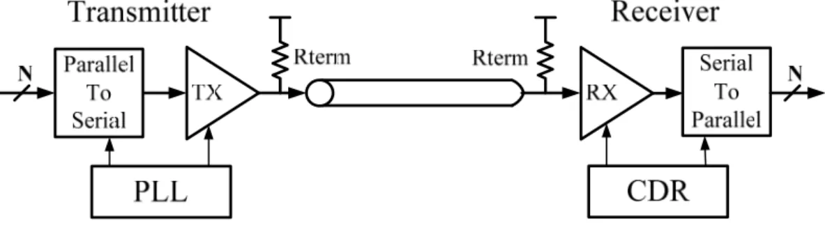
3.1 Introduction
A general serial link is shown in Fig. 3.1. There are three primary components in this architecture which are transmitter, cable, and receiver [16][17]. The input data are usually parallel data stream in order to increase the bandwidth of the link. Therefore, we need a PISO (parallel in serial out) circuit to convert digital bits into differential bit stream. Then, the serial data are sent through transmitter driver to the cable. In the receiver end, it recovers the signal to the original digital bits from cable by amplifying and sampling the signals. The CDR (clock data recovery) circuit embedded in the receiving side adjusting the receiver clock based on the receiver data to sample the center of the data eye. Then, a SIPO (serial in parallel out) circuit converts the serial
data back to N parallel bits. This dissertation focuses on the transmitter end and cable. We introduce the detail components in the following section.
Fig. 3.1Tranceiver architecture
3.2 The Architecture of Serial ATA Transmitter
Fig. 3.2 shows the architecture of the SATA transmitter. This architecture is composed of transmitter and PLL. The circuit elements designed in this dissertation are in dotted blocks. This transmitter starts with two kinds of input parallel data streams, which are K28.5 and PRBS (Pseudo Random Binary Sequence) selected by AMUX. Through K28.5 pattern we can test and verify if the output data streams meet with input data or not. And we can measure the output data eye diagram via PRBS pattern. Then the input patterns are delivered to BMUX. BMUX selects the first five or last five parallel data transmit to PISO cycle by cycle. In order to transmit data in high speed link, we use 5-to-1 PISO circuit. This circuit converts the parallel data streams into serial data streams by using 1.2 GHz 5 phase clock. After all, CML driver transmits 6Gbps serial data into cable. Besides, we can compensate the large loss of cable by using tunable pre-emphasis circuit. According to different cable length with different data rate, we can choose the suitable pre-emphasis amount.
Section 3.3 will show the design of K28.5 and PRBS encoder, the synchronization and PISO architecture, CML and pre-driver architecture, and a tunable pre-emphasis filter decided concept.
Fig. 3.2 Transmitter architecture
3.3 Functional Blocks of Transmitter
3.3.1 PRBS and K28.5
The PRBS circuit works as a data generator. The function of the PRBS is to generate random data in a long term period. It means there is the same numbers of the ones and zeroes during the long term period and it will make the power spectrum density more evenly distributed. It generates all possible patterns without all 0 patterns. The maximal length sequence is 2N-1. In order to implement ten parallel inputs, a 210-1 data pattern is generated with 10 registers and XOR circuits. We design
the ten bits PRBS encoder with each 600MHz data rate to get a 6Gbps of system operational speed. We use a control signal to provide a pulse signal (logic one) to restart the circuit to generate the parallel data. A 600MHz clock is also needed to trigger the register.
Another input pattern is K28.5. This pattern is commonly specified for jitter measurement in Fiber Channel and Ethernet systems operation. We use this pattern to verify that the circuit can transmit data correctly into cable and the output eye diagram can fit the SATA specifications.
The K.28.5 pattern has two sequences (composed of alternating K28.5+ and K28.5-), the positive disparity (0011111010) and the negative disparity (1100000101). These two sequences form the symbols 00111110101100000101. These long symbols contain five consecutive 1's and five consecutive 0's, (the longest DC data). It also contains an isolated 1-010-and an isolated 0-101, (the high speed AC transition).
3.3.2 AMUX and BMUX
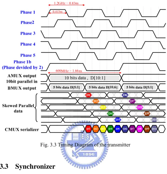
In order to gain the bandwidth of the circuit, we use two MUX circuits shown in Fig. 3.3. AMUX is composed of 10 sets of 2-to-1 MUX which select the PRBS or K28.5 input pattern. The ten parallel input data are divided into two groups by BMUX, this is for high speed considerations shown in Fig. 3.3. The 10 bits data are divided into first 5 bits data and last 5 bits data by a half speed clock phase 1b. Then, these 5 bits data are transferred into synchronizer circuit. The synchronizer circuit will skew the parallel data by the different phase and the PISO circuit will sample each data into serial stream to transmit to the CML data driver.
Fig. 3.3 Timing Diagram of the transmitter
3.3.3 Synchronizer
The parallel data from BMUX should be shifted to fit the sampling time of PISO multiplexer, therefore, we need a synchronizer circuit to skew the parallel input data which makes the PISO circuit sample the parallel data one by one in the middle point correctly and gain enough time margin [18]. Fig. 3.4 shows the synchronizer function block. The synchronizer is used to skew the data differs with 1/5 period of data cycle time which equal 166ps. Then the parallel data are sampled by PISO circuit to transfer 6Gbps to the cable. From this figure we can find out that we also need a PLL circuit to generate multi-phase clocks for the synchronizer. The detail circuit design issue is described in the next chapter.
B5 B4 B3 B2 BMUX output B1
Synchronizer
D5 D4 D3 D2 D1 Multi-Phase 830ps 166ps Sync output 1.2GHz 5 phase clockFig. 3.4 Synchronization function block
3.3.4 CMUX
CMUX is need as PISO (serializer) to sample the skewed parallel data D1~D5 and serialize the data into CML data driver. Because of the operation of the synchronizer, each parallel data will be sampled at the middle to prevent sampling the wrong data. Fig. 3.5 shows the timing diagram of CMUX. Each parallel data will be controlled by two clock phases, take the D1 (the first bit parallel data) as an example. It will be sampled when both of the clk1(phase1) and the inversion of clk2(phase2b) are logic high. It means each serial output data has a 1/5 period which is the overlapping between two clock phases. Fig. 3.6 shows the architecture of the CMUX, they are composed of five pairs of differential paths, and each serial data is sampled and delivered by logic driver block. Logical driver is a CML like circuit which can transmit serial data in high speed. The detail circuit of logic driver is described in next chapter.
D3 D2 D1 clk1 clk2b Parallel DATA 1/5 period D1 D2 D3 Serial DATA D4 D5 Fig. 3.5 PISO timing diagram
Fig. 3.6 PISO architecture
3.4 Pre-emphasis
The purpose of Pre-emphasis is to compensate the cable loss. Cable acts like a low pass filter function, and a pre-emphasis circuit is like a high pass filter function. Thus in the receiver end, the frequency response is flattened like an all pass filter function and the eye amplitude is enhanced to meet our specifications. A FIR
filter-based pre-emphasis can counteract inter-symbol-interference (ISI) in high speed serial link data transmission [19][20].
3.4.1 Overview
As the data rate up to Gbps range due to the limitation of the interconnect bandwidth, the propagation of the signaling from transmitter to receiver is mainly affected by the effect which called inter-symbol-interference (ISI). ISI is caused by channel bandwidth limitations due to impairments of physical backplanes, such as dielectric loss, skin-effect, package effect, incident and reflection. This effect may cause the far-end receiver eye become too close to be recovered via the CDR block and cause large bit error rate. Fig. 3.7 shows how the ISI distorted the signaling. The attenuation reduces the series of data amplitude by more than 20%. Furthermore, lower frequency attenuation causes the signal’s long setting tail. This is because the cable attenuation of the low frequency and high frequency is not uniform. From Fig. 3.8(a) we can find out that there is a small open receiver eye, this is because the high frequency components are attenuated. The way to overcome the signal integrity and the cable bandwidth is to compensate for the cable frequency response. One of the methods is using pre-emphasis circuit. A pre-emphasis circuit using a Finite Impulse Response (FIR) filter can either pre-shapes the signal in the transmitter and flatten the frequency response in the receiver. It makes the low frequency and high frequency response in the uniform gain amplitude.
In order to get a correct data and meet with the SATA specification, we use pre-emphasis circuit to pre-shape the signal in transmitter to compensate the cable frequency response. Fig. 3.8(b) is an example of using pre-emphasis to have a better
eye.
(a)
(b)
Fig. 3.7 (a) The input signal in the transmitter (b) The output signal in the receiver
(a)
(b)
Fig. 3.8 Signaling waveform (a) without pre-emphasis (b) with pre-emphasis
0 0 1 ( ) (1 ) V ( )in N i V (in ) i V n a n a n i = = + ⋅ −
∑
⋅ − (3-1) 0 1 ( ) V ( )in N i V (in ) i V n n b n i = = −∑
⋅ − (3-2) The FIR pre-emphasis design usually involves the determination of the required number of taps and the optimization of tap coefficients. Eqn. (3-1) is used to enlarge the high frequency component and Eqn. (3-2) is used to suppress the low frequency component. Input V ( )in n means present signal symbol andV (
inn i
−
)
means thepast transmitted symbols which affect the present symbol V ( )in n . Coefficient
a
iandi
b
are the magnitude of each tap coefficients. Therefore, the coefficientsa
i,b
iand the past N symbol affect the output amount
V
0.V
0 is the sum of the presentsymbol V ( )in n and past N symbol
V (
inn i
−
)
,i
=1 to N. We combine the twoequation into Eqn. (3-3).
0 0 1 ( ) V ( )in N i V (in ) i V n a n c n i = = −
∑
⋅ − (3-3) There are two implementations to realize the pre-emphasis method. The first method shows of a N-tap transmit filter was designed by MIT group, Dally and Poulton [11] In the architecture, all the FIR filter calculations are done by digital adders implemented with a look up table and a digital-to-analog converter (DAC) generates the output pulse. Fig. 3.9 shows this implementation with a 5-tap filter. In order to overcome the speed limitations of the process, this circuit use drivers in parallel, and therefore each branch requires separate digital logic. The digital logic modules, having the present and the five previous bits, calculate the amplitude of the current pulse that should be transmitted. This is a digital type of pre-emphasis method. The circuit adjusts the pre-emphasis amount according to the input parallel data. Thisimplementation incorporates a FIR pre-shaping filter into a differential transmitter, and transmits 4Gbps serial data through cable to the receiver.
The second method shows an N-tap transmit with an analog type technique to realize the pre-emphasis filter was designed by Stanford group, Farjad-Rad[12]. In this implementation, the FIR N-tap complex filter is merged into each DAC driver module. The high-resolution DAC drivers are also replaced by 1-bit drivers for each filter tap. The architecture of this approach is shown for 4-tap filter in Fig. 3.10. Each module uses the present and 3 previous bits to generate the complete pre-shaped pulse over 4 bit periods directly and independently of all previously transmitted symbols. Finally, the individually pre-shaped symbols are adjusted by the current source amount of main driver and pre-emphasis driver. This implementation summed the output amplitude at the transmitter, and transmits 10Gbps data over 10-meter cable.
Distribute and retime
Filter 3bit DAC
5
Filter 3bit DAC
5
Filter 3bit DAC
5 φ9 φ0 High-speed output 4 Gbps 400MHz D0-9 3 3 3 Fig. 3.9 Block diagram of a pre-shaping parallel transmitter for MIT group [11]
Fig. 3.10 Block diagram of a pre-shaping parallel transmitter for Stanford group [12] However, in the first implementation, each driver module is a 3-bit DAC to reduce the quantization error of the FIR filter. When operating at high frequency data rate, the combination of these digital filters and high-resolution DACs makes the transmitter circuit quite complex and consume many power. On the contrary, the second implementation removes the complex digital filter and simply sums the input filter values which are performed by multiplying and summing the analog currents in the analog domain. So we can simply adjust the pre-emphasis amount by sizing the MOS of the current source. Therefore, we choose the second method to implement our SATA transmitter.
3.4.2 Methodology and Design
The pre-emphasis circuit works like a FIR filter to enlarge the high frequency component so that the receiver signal amplitude for differential transition is fixed. There are three parameters to design a FIR filter, the tap number, the coefficients and the tap delay time. In a high speed data rate driver with high loading, using tap number higher than two will consume lots of area and power consumption [13]. Thus,
coefficients and tap delay time are two feasible parameters to adopt for different pre-emphasis conditions.
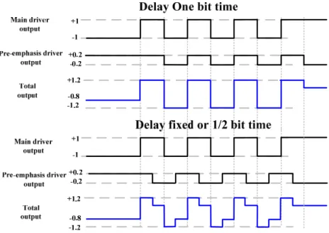
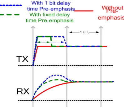
In time domain, we assume that when total output amplitude is 1.2V then the circuit can compensate for the cable loss for a correct receiver eye. We can find out that there are two ways to enlarge the TX signal shown in Fig. 3.11. One is when pre-emphasis output delay one bit time, the other is when pre-emphasis output delay fixed or half bit time. In order to investigate these two kinds of pre-emphasis, we implement two types of pre-emphasis into our transmitter. From Fig. 3.12, we can find out that without pre-emphasis, receiver amplitude is decayed and has a long tail (ISI). With either of our proposed pre-emphasis mechanism, it can cancel the cable loss and compensate the receiver rising time. Moreover, the main driver and the pre-emphasis driver (strength and their relative times) can be tuned such that it can be tuned for different cable length to fit the SATA specification. When the transmitter operates in different data rate, we can choose the better pre-emphasis mechanism to compensate for the cable loss.
Fig. 3.12 Signaling in TX RX and ISI cancellation
The frequency response of traditional transmitter is shown in (a). It has different signal amplitudes in the receiver node and the eye amplitude is different for different cables. In order to implement high data rate mechanism, [14] proposed another method shown in (b). The advantage of this method is that the circuit have the constant receiver signal amplitude for a different cable length but it need to decide one more coefficient (a0) shown in Eqn. (3-3).
Fig. 3.13 Frequency response of the transmission with pre-emphasis
In our method, we keep
a
0 equals to 1 N i i a =∑
to gain higher uniform gain. The dotted line in Fig. 3.13 means the overall frequency response. The advantage of our method is that we have constant receiver signal amplitude even for a different cable length but it needs to decide one more coefficient (a0). It means the currentsource of our transmitter driver need to be enlarged with a pre-emphasis circuit. We use only one tap (N=1) pre-emphasis for our transmitter circuit. Eqn. (3-4) shows the equation of one bit delay time pre-emphasis, and Eqn. (3-5) shows the half bit time pre-emphasis. The difference between these two equations is the sampling frequency.
0( ) 0V ( )in 1 V (in 1)
V n = a n − C ⋅ n − 0 <
t < T/2
0V ( )in
a n
=
T/2
<t < T
(3-4) The FIR coefficient a1 and c1 shown in Eqn. (3-4) represents the current sourcemagnitude such as IS and I1 shown in Fig. 3.16. The overall frequency response with
the package and cable is shown in Fig. 3.14. Take 5 meter cable as an example, we can see the bandwidth is 1.3GHz, and we make the main driver and tap1 magnitude to be 16mA (IS) and 6.4mA (I1). Then we normalize the current magnitude and we set
the FIR coefficient a1 and c1 as [1.28 -0.28]. In this case, FIR filter can gain 3.8dB
under 5m length cable, thus we can make sure that the total bandwidth can be 3GHz. For 10m cable length, we can see that the bandwidth is 400MHz. In order to gain the bandwidth to 3GHz, we determine the normalized FIR coefficient to be [1.53 -0.53]. The frequency response of FIR is shown in Fig. 3.15. We can see that the high pass filter for 10m cable has larger gain and can compensate the bandwidth to 3GHz.
Fig. 3.14 Total frequency response without pre-emphasis
(a) (b) Fig. 3.15 Frequency response of one bit delay time FIR for (a) 5m (b) 10m cable
3.4.3 Architecture and Comparison
Fig. 3.16 shows the driver block diagram including the main driver and tap1. We implement the tunable pre-emphasis mechanism via a CMLMUX circuit [10]. Through this MUX we can select either fixed delay time pre-emphasis or one bit
delay time pre-emphasis. In this way, the signal amplitude in the receiver is the same for different cable length and different delay time. Through this mechanism, we can also transmit data from 3Gbps to 6Gbps and select the suitable pre-emphasis circuit to compensate for the loss of the different length cable. We describe the methodology of these two types of pre-emphasis in the following.
Fig. 3.16 CML driver and pre-emphasis driver
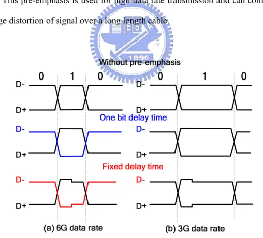
Fixed delay time (FDT) pre-emphasis:This pre-emphasis can compensate for fixed amount of cable loss during different data rate. We implement this method by inserting two CML buffer in the pre-emphasis circuit. Each buffer has 30ps delay time and the first buffer also included a tunable delay time function which can produce 40ps delay range [15]. Therefore, FDT pre-emphasis can produce 80~120 delay time. In our proposed transmitter, the data rate is 166ps (6Gbps). For comparing with OBT pre-emphasis, we design the fixed delay time close to 83ps which is a half of bit time for 6Gbps. From Fig. 3.17(a) (b), we can find out that this pre-emphasis amount is fixed during different data rates. This kind of pre-emphasis is used for less attenuation of cable and for low speed data rate. It can compensate data with low power consumption and enhance the receiver eye amplitude with low ISI effect. The
disadvantage of this FDT pre-emphasis is that it causes more jitter when the circuit operated in high speed.
One bit delay time (OBT) pre-emphasis:This pre-emphasis always compensate a full one bit time amount for different data rate. This kind of pre-emphasis can make receiver eye open with less jitter. However, when the data rate is 3Gbps, it will make a big overshoot in the receiver eye. As shown in Fig. 3.17 (a) (b), we can find out that when the circuit operated in 3Gbps, the pre-emphasis still pre-shaped the signal during the bit period. This makes unnecessary pre-emphasis amount and cause ISI effect. We implement this method by inserting a replica circuit such as PISO and data driver. This pre-emphasis is used for high data rate transmission and can compensate for large distortion of signal over a long length cable.
3.5 Summary
In this chapter, we describe the architecture of the proposed transmitter. The input pattern of data, PRBS and K28.5, are general data patterns for testing and verifying with the SATA specification. The tunable pre-emphasis concept is also introduced and we describe the difference between OBT and FDT pre-emphasis. In the next chapter, we will describe the detail circuit design and show the simulation results of our proposed transmitter.
Chapter 4
Serial ATA Transmitter Circuit
Design
4.1 Introduction
This chapter describes the serial ATA transmitter circuit design concept and the detail circuit of the proposed architecture. The transmitter circuit includes the data generator, PISO, tunable pre-emphasis, data driver. The circuit implementation and simulation will be described in the end of this chapter. We use TSMC1P6M 0.18um to implement the serial ATA transmitter. The data rate of the transmitter is 6Gbps for 1~10m cable and the clock rate on chip is 1.2GHz. The tunable pre-emphasis circuit can adjust the pre-emphasis amount with different delay time due to the user’s data rate.
4.2 Transmitter Design Issues
Rterm Ω 50RX
CDR Coxial Cable Ω 50 R 1.2GHzTX
10 PLL 5 PAD L Cout Cin 2n 1p 0.5p PAD L Cout Cin 2n 1p 0.5p Rterm Ω 50Fig. 4.1 Transceiver architecture
Fig. 4.1 shows the high-speed link transceiver architecture. The chip package interface, termination resistance and cable are also included in the figure. Cin is the internal pad parasitic capacitor and Cout is the loading of PCB and package. L is the bonding wore between chip and PCB. The characteristic impedance of cable equals to Rterm and is denoted as R. In our circuit, we use typical value of Rterm=R=50Ω, Cin=0.5pF, Cout=1pF and L=2nH for simulation. The frequency response of the package is shown in Fig. 4.2, the f-3dB=5Ghz. In this dissertation, the RX and CDR are
not included in the simulation. Fig. 4.3 shows the frequency response of coaxial cable with the HSPICE model and with measurement result. We use RG233/U as the coaxial cable with characteristic impedance is 50Ω.
Fig. 4.2 Frequency response of package 106 107 108 109 -12 -10 -8 -6 -4 -2 0 2.5 GHz -7.4 dB 1.6 GHz 5 m (measurement) 5 m (simulation) 10 m (simulation)
Ga
in
(d
B)
Frequency(Hz)
400 MHz -3.7 dBFig. 4.3 Frequency response of coaxial cable
4.3 Circuit Design and Simulation Results
This section describes the circuit design of the proposed transmitter and their simulation results. The simulation results include the parasitic of the package, and the
4.3.1 Input Data
The input data is from PRBS or K28.5 pattern. The PRBS is built on chip and generates random pattern automatically by the registor and XOR circuit shown in Fig. 4.4. In order to implement ten parallel inputs, a 210-1 data pattern is generated with 10 registers and XOR circuits. We design the ten bits PRBS encoder with each 600MHz data rate to get a 6Gbps of system operational speed. The control signal Vsela provides a pulse (logic one) to restart the circuit to generate the parallel data. A 600MHz clock is also needed to trigger the register. The simulation result is shown in Fig. 4.5. DFF1 D Q S DFF2 D Q S DFF3 D Q S DFF4 D Q S DFF5 D Q S CLK DFF6 D Q S DFF7 D Q S DFF8 D Q S DFF9 D Q S DFF10 D Q S Vsela
Pin1 Pin2 Pin3 Pin4 Pin5 Pin6 Pin7 Pin8 Pin9 Pin10
Fig. 4.4 10-bit PRBS encoder
The K28.5 is a worst case regular pattern generated to verify if the circuit can transmit the data correctly or not and if the RX eye can fit the SATA specification or not. The K28.5 pattern has two sequences (composed of alternating K28.5+ and K28.5-), the positive disparity (0011111010) and the negative disparity (1100000101). These two sequences form the symbols 00111110101100000101. These long symbols contain five consecutive 1's and five consecutive 0's, (the longest DC data). It also contains an isolated 1-010-and an isolated 0-101, (the high speed AC transition). Thus, we implement this circuit by the XOR circuit. With input VDD/GND and 300MHz
clock, we can generate the positive or negative disparity. The simulation result is shown in Fig. 4.6. Pin1 Pin2 Pin3 Pin4 Pin5 Pin6 Pin7 Pin8 Pin9 Pin10
Fig. 4.5 Simulation waveform with 10-bit PRBS encoder
Tx_out
0 0 1 1 1 1 1 0 1 0 1 1 0 0 0 0 0 1 0 1
0 0 1 1 1 1 1 0 1 0 1 1 0 0 0 0 0 1 0 1
Time (ns)
Voltage(v)
Voltage(v)
Fig. 4.7 Simulation waveform with K28.5 and PRBS input patterns
We simulate the two kinds of input pattern shown in Fig. 4.7, and we measure the input data from the transmitter output to verify the K28.5 pattern can be correctly sampled and transferred. The figure also shows the single and differential serial data. The beginning 9ns is K28.5 pattern and then we changed into PRBS pattern. We can find out that K28.5 is a fixed and repeated pattern, and the PRBS is a random input pattern. Therefore, we can select these two kinds of input pattern any time we want.
4.3.2 Synchronizer
In order to sample each five parallel data, the data should be skewed to fit the sampling time margin of PISO circuit. Thus, the synchronization circuit is design by register with multi-phase clocks as shown in Fig. 4.8. In our design, we use True Single Phase Circuit (TSPC) type DFF as the register to enhance the speed when implementing the skewed data. The register are triggered by the five 1.2GHz clock phase and the phase offset is 166ps. The input data B1~B5 are sampled and stored in the registers, and then sequentially transferred into PISO circuit with different clock
phase. With consideration of setup and hold time of registers, we all use clk1 to sample data in the first stage registers, and the second stage registers sample the data with successive clocks. Thus, we choose clk3, clk4, clk5, clk1 and clk4 so that the registers can finish the operation in the correct period interval and data can be sampled correctly as shown in Fig. 3.3..
B5 B4 B3 B2 BMUX output B1
Synchronizer
D5 D4 D3 D2 D1 Multi-Phase 830ps 166ps Sync output 1.2GHz 5 phase clock Reg Reg B1 CLK1 CLK3 D1 Reg Reg B2 CLK1 CLK4 D2 Reg Reg B3 CLK1 CLK5 D3 Reg Reg B4 CLK1 CLK1 D4 Reg Reg B5 CLK1 CLK4 D5 Reg CLK2 Fig. 4.8 5-bits data synchronizer4.3.3 PISO
The PISO architecture is shown in Fig. 4.9 and each logic driver circuit is described in Fig. 4.10. It is composed of five pairs of differential paths with a PMOS added in each path to pre-charge the internal node to high level before logic high is sent out and with an active load NMOS to enhance the circuit bandwidth. For an example, we employ the difference between clock phase1 and phase2b to transmit one branch of data shown in our logic driver. However, the driver may suffer some charge sharing effect shown in Fig. 4.10. The effect includes two kinds of source. The first one is to pull down the output signal level when M1 is turned on. The other one will
turned on. To reduce these two effects, we add a clk5 to control the turn-on of M2. In this way, M2 and M1 will turn on simultaneously. So the two effects will cancel each other. Therefore the serial data can be correctly transmitted into CML driver. Fig. 4.11 shows the simulation results of the output driver without and with charge sharing compensation.
Fig. 4.9 PISO circuit
(a) (b)
Fig. 4.11 Charge sharing effect [14] (a) without charge compensation (b)with charge compensation
4.3.4 Pre-emphasis and Data Driver
Fig. 4.12 shows our pre-emphasis architecture. According to different data rate, we can select half bit time and 1 bit time pre-emphasis by CML MUX circuit. For half bit delay time 83ps, we generate this delay by using two inverters. This kind of pre-emphasis amount is fixed for different data rate. Thus, we can guarantee that the transmitter circuit won’t transmit data with over pre-emphasis amount. For 1 bit delay time 166ps, we implement this method by design a replicate circuit which has PISO and tap buffer. When circuit operated in the high data rate and we want to get a perfect eye diagram in the receiver end. We use CML MUX to select this mode to meet with the SATA specification.
Fig. 4.12 Pre-emphasis and data driver architecture
FDT pre-emphasis: We implement this method by inserting two CML buffer in the pre-emphasis circuit. Each buffer has 30ps delay time shown in Fig. 4.13 (a) (b). In order to realize the tunable delay time mechanism, we use a different type of circuit shown in Fig. 4.13 (a) [15]. By inserting a negative resistance which is a positive feedback circuit to the output, this circuit can produces a delay range from output to input by changing the equivalent R to alter the RC-delay. We control the value of the equivalent resistance by the voltage VB1 and VB2. The differential control voltage VB1 – VB2 divides the total bias current between the input differential pair and negative resistance pair. If VB1 » VB2, the delay time is minimized such as a typical CML Buffer and the output swing remains constant as the total bias current through the output resistors is fixed. The required tuning range of the tunable CML buffer depends on the two things which are desired symbol length and the necessary duty-cycle range for pre-emphasis. Therefore, we design the tunable CML buffer to
produce 30~70ps delay range. Therefore, FDT pre-emphasis can be tuned from 80 to 120 delay time.
(a) (b)
Fig. 4.13 FDT Pre-emphasis detail circuit (a) Tunable CML buffer (b) CML buffer OBT pre-emphasis:We implement this method by inserting a replica circuit such as PISO and data driver. The PISO circuit is described in the previous section and the CML buffer is the same as Fig. 4.13(b). OBT pre-emphasis can precisely generate one bit delay time under different data rate.
Either FDT or OBT pre-emphasis can be selected by CML MUX. The circuit is shown in Fig. 4.14 (a) [22]. It like two CML buffers which share the same current source. We use Vb1 and Vb2 to select one of the two pre-emphasis. For example, when Vb1 is high and Vb2 is low, the FDT pre-emphasis is selected and the left path of the CML MUX is turned on to transmit data into CML. At this moment, the other pre-emphasis can be turned off to save power consumption. Fig. 4.14 (b) is CML circuit which we have described in the previous chapter. We can control the CML current source of main driver and tap1 to enlarge the TX/RX eye diagram and make the constant receiver signal amplitude to fit the SATA specification. The overall circuit simulation results are described in the next section.
(a) (b)
Fig. 4.14 CML MUX and CML driver circuit (a) CML MUX (b) CML Driver
4.4 Simulation Results
Fig. 4.15 shows the output node name of transmitter The termination of transmitter and receiver is 50Ω. We use W model in HSPICE to simulate the RG233/U cable model and we can modify the cable length for different case. The following simulated diagrams are the post layout simulation results under 6Gbps data rate. Ω Ω Ω Ω Ω Ω
Fig. 4.15 The simple diagram of TX and RX
We design the input voltage of pre-driver and pre-emphasis to be 1.8V to 0.8v as shown in Fig. 4.16, the jitter are 10ps with a large input swing. This input signal can provide CML data driver a correct and large input swing to enhance the signal quality.
Voltage(v)
Fig. 4.16 The simulation results of Vin+/- and CML+/- node
Fig. 4.17 shows the simulation results of RX_out node under 1m cable length. The jitter is about 10ps and the amplitude is 600mV.
Time (s)
10ps
Fig. 4.17 The eye diagram of receiver in RX_out node (cable length=1m)
4.4.1 FDT and OBT pre-emphasis comparison
In this section, we set the delay time of FDT pre-emphasis to half bit time (83ps) for 6Gbps. Then we can compare the two kinds of pre-emphasis. Fig. 4.18 shows the post-layout simulation waveform with FDT and OBT pre-emphasis in CML and ECML node. In Fig. 4.18 (a), the differential voltage of ECML node delays half bit
half bit time after CML node. Therefore, we have two kinds of pre-emphasis which are half bit time and one bit time pre-emphasis under 6Gbps data rate.
(a)
(b)
Fig. 4.18 The simulation results of CML and ECML node (a) FDT (b) OBT Fig. 4.19 shows the post-layout simulation waveform with FDT and OBT pre-emphasis in RX node under 6Gbps data rate with 5M cable. We can find out that FDT compensate less pre-emphasis amount under high speed data rate. Therefore, in this case we shall choose one bit time pre-emphasis for transmitting data. However, when the data rate is down to 3Gbps as shown in Fig. 4.20, we find out that the OBT pre-emphasis will cause 230mV overshoot in the receiver eye diagram and this overshoot will enlarge the jitter in the receiver eye diagram. Both of the amplitudes are 630mV and jitters in FDT/OBT pre-emphasis are 18/16ps. Thus, in 3Gbps data rate, we choose FDT pre-emphasis to improve the signal quality in the receiver end. The comparison of these two pre-emphasis is summed in Table 4.1. We compare the power, jitter and eye amplitude with different data rate.
CML
node
ECML
node
CML
node
ECML
node
83ps 166ps
Fig. 4.19 RX-eye with fixed and 1 bit delay time pre-emphasis under 6Gbps
Fig. 4.20 RX-eye with fixed and 1 bit delay time pre-emphasis under 3Gbps
Table 4.1 Pre-emphasis performance comparison (Cable length =5M) Data rate 6Gbps 3Gbps Transmitter swing 700mV 700mV
Receiver swing 550mV 630mv Receiver jitter (FDT/OBT) 27/14ps 18/16ps
Total power (with FDT) 105mW 90mW Total power (with OBT) 115mW 100mW
is because the implementation of the tunable methodology. In order to investigate the different delay time affect the pre-emphasis amount, we have to use the inverter train type pre-emphasis to implement the tunable mechanism. For a low jitter FDT pre-emphasis, we can use the methodology like OBT type. This can be done by inserting replica circuit of PISO and data driver, then data are sampled by different phase to implement fixed amount pre-emphasis. The RX eye is simulated in the Fig. 4.21. The jitter is reduced to 14ps and the swing is the same as FDT pre-emphasis.
Fig. 4.21 RX-eye with modified half bit delay time pre-emphasis under 3Gbps
Fig. 4.22 shows the waveform with and without pre-emphasis in the RX node under 10m cable. Obviously, the amplitude without pre-emphasis (160mV) is smaller than 200 mV and does not fit with the SATA eye mask. With our proposed pre-emphasis, the output signal amplitude is enlarged and fit with the SATA specification. In this case, FDT/OBT pre-emphasis can enlarge the magnitude by 300/410mV. Therefore, our proposed transmitter can transmit data under 1m~ 10m cable.
Fig. 4.22 The eye diagram of receiver (cable length=10m) Table 4.2 Simulation results summary of the transmitter
Technology 0.18 um 1P6M CMOS Supply voltage 1.8V
Clock rate 1.2GHz (5 phase) Data rate 6 Gbps Cable lenth 1~10 公尺 Transmitter output swing 700mV
Receiver input swing 550mV
Total power (without pre-emphasis) 72 mW Total power
(with FDT pre-emphasis ) 105 mW Total power
(with OBT pre-emphasis ) 115 mW
Table 4.3 shows the comparison between our design and other papers [12] [18] [20] [21]. When compared with the paper of JSSCC 2004, our circuit consumes lower power to achieve high data rate and high output voltage swing. When compared with
other papers, we can find that our transmitter can save more powers when operated at high data rate and high voltage swing.
Table 4.3 Comparisons of the performance between our design and other papers
Our Work JSSC 2004[21] ASPDAC 2003[18] JSSC 2005[20] JSSC 2000[12] Technology 0.18 um 0.18um 0.18um 0.11um 0.3um
Data Rate 6Gbps 5Gbps 5Gbps 6.4Gbps 8Gbps Output Voltage Swing 700mV 600mV 200mV 104mV 350mV Power Consumption (w.o. PLL) 115mW 120mW 150mW 150mW 220mW Supply Voltage 1.8V 1.8V 1.8V 1.2V 3V
4.5 Summary
In this chapter, we describe the detail circuit of the proposed transmitter. The simulation results are also shown in this chapter. We use PRBS and K28.5 as the input pattern to test and verify with the SATA specification. The simulation result of TX and Rx eye diagram are met with the specifications. The OBT and FDT pre-emphasis are also discussed and simulated in this chapter. The length of the coaxial cable can be in the range of 1 meter to 10 meter and for data rate of 3Gbps and 6Gbps. In the next chapter, we will describe the experimental considerations and show the measurement results of our proposed transmitter.
Chapter 5
Experimental Results
5.1 Layout and Experimental Setup
The transmitter chip is implemented in TSMC 0.18um 4P6M CMOS process. Fig. 5-1 shows the layout of the transmitter. The area of the chip (including the bonding pads) is 1160 x 1280 um2. The area of transmitter (without PLL) is 630 x 320 um2. The power supply noise would be the major concern in the layout. Therefore, we separate the transmitter circuit as three parts, PLL, digital of TX and analog of TX. The power lines of the three parts are independent. Double guardrings are placed in every blocks of the circuit to reduce the substrate noise. The decoupling capacitance is also placed as much as we can to stabilize the power line and reference voltage around the circuit. The phase generated from PLL to transmitter is the most sensitive metal line in the layout. The distance and length of each phase is treated in the same condition. We also insert the buffers du ing the long distance of metal line to enhance the driving capability.
Fig. 5.1 shows the layout view of the transmitter with the major functional blocks. There are transmitter with pre-emphasis, SSCG based on PLL and adaptive termination. The number of total pads is 38. (Including transmitter, adaptive termination, SSCG and decoupling capatiance)
Transmitter
with pre-emphasis
SSCG
based
on PLL
Adaptive terminationTransmitter
with pre-emphasis
SSCG
based
on PLL
Adaptive terminationFig. 5.1 Transmitter layout
The experimental setup for transmitter is shown in Fig. 5.2. First, we use Pulse Pattern Generator (Agilent 81130A 660MHz) to generate the reference clock of PLL. Then, the PLL output clock signal is fed to Digital Storage Oscilloscope (Tektronix TDS6124C 12GHz) to view the waveform. We can also use the PSA series spectrum Analyzer (Aglient E4440A 26GHz) to measure the spectrum of the PLL and the TX. The differential outputs of TX and the eye diagram are measured through the Wide Bandwidth Oscilloscope (Aglient 86100B 20GHz). Thus, we can verify the accuracy of the input pattern.
![Fig. 2.2 Physical Plant Overall Block Diagram [4]](https://thumb-ap.123doks.com/thumbv2/9libinfo/8223592.170645/17.892.159.756.539.1109/fig-physical-plant-overall-block-diagram.webp)