利用電荷幫浦分佈法研究深次微米 N 型 MOS 元件電漿製程傷害之可靠性
Analysis of the Plasma Damage in Deep-submicr on nMOSFET’s by Using
the Char ge Pumping Pr ofiling Technique
計畫編號:NSC 89-2215-E-009-107
執行期限:89 年 08 月 01 日至 90 年 07 月 31 日
主持人:莊紹勳 國立交通大學電子工程學系
一、中文摘要 現今半導體製程中,電漿蝕刻技術已 成為不可或缺之生產技術,它是透過高能 電漿離子直接撞擊,或是利用電漿離子氣 體與晶圓表面起化學反應,而達成蝕刻的 目的。然而,近年來發現這種蝕刻方式會 對高積體化的電路佈局造成天線效應,並 引發可靠性問題。一般來說,電漿蝕刻傷 害的類型可分為兩種: 其中一種發生在通 道區域或是閘氧化層內部的電漿充放電傷 害(plasma charging damage, PCD)﹔另外一 種發生在閘及邊緣區域的電漿邊緣傷害 (plasma edge damage, PED)。以往都著重於 前者,而對後者的研究較少。本計劃著眼 於此,即針對此電漿邊緣傷害對於短通道 元件的可靠性問題,提出一套研究分析方 法。 在本計劃中,我們即針對電漿邊緣傷 害(PED)進行研究,利用電荷幫浦空間分 佈法分析電漿蝕刻傷害及其引發的可靠性 問題。本研究將此電荷幫浦分佈法,首次 的應用於局部性的電漿蝕刻傷害研究上。 此套分析法不但可以直接評斷電漿傷害 外,並且可以克服傳統研究方法(如: 基本 CP 法與 GIDL 法)不夠準確及直觀的缺 陷。本計劃所得到之重要結論包含: (1)藉 由電荷幫浦分佈法配合 HC stress,首次的 應用於電漿蝕刻造成閘極邊緣傷害的研究 上。此法將可取代國外發展之基本 CP 法 與 GIDL 法。 (2)三種基本特性量測(包含 不同區域之電漿蝕刻傷害,及不同天線結 構,以及不同通道長度之電漿蝕刻傷害測 定),運用電荷幫浦空間分佈法完成電漿蝕 刻傷害退化之評估。 (3)以區域性電漿蝕 刻傷害的觀點,建立電漿蝕刻造成的閘極 邊緣傷害的機制與其物理模式。 (4)利用 雙峰值的電漿蝕刻傷害分佈結果,證實了 吾人提出之“電漿放電導致邊緣傷害”將主 導元件的可靠性。 關鍵詞:金氧半元件可靠性,電漿蝕刻傷 害,電漿邊緣傷害,熱載子可靠性,電荷 幫浦分佈法。 Abstr actPlasma etching process has become a major fabrication technique in modern IC manufacturing. The dry etching process is performed by using a high-energy plasma ion to directly bomb Si-wafer or the plasma ion gas to interact with the Si-wafer. However, in recent years, this etching process has been found to cause the antenna effect and to degrade device reliability for the high-density circuit. The plasma damage can be classified into two categories: the first one is plasma charging damage, which occurred in the channel region; the other one is plasma edge damage, which generated at poly-Si gate edge region. In the previous studies, most of them were focused on the former. Therefore, in this study, we will investigate the plasma edge damage and provide a new analysis method.
In this work, we used the charge pumping profiling technique to analyze the plasma damage and the associated hot carrier degradation. For the first time, this profiling technique has been used for the study of plasma damage. This technique can monitor the plasma damage more directly and precisely than the conventional method,
such as basic CP method and GIDL method. Several important results have been drawn from this study. First, based on the charge pumping profiling technique and the HC stress, the plasma edge damage has been studied. This technique can be used to replace the conventional CP measurement and the GIDL methods. Second, by using this technique, three kinds of plasma damage measurements have been performed. Third, from the observed localized plasma damage, the degradation mechanism for the plasma edge damage has been performed. Fourth, from the results of the two-peak profile of interface state distribution, the plasma charging enhanced edge damage will dominate device reliability.
Keywords: MOSFET device reliability,
plasma damage, plasma etching damage, plasma edge damage, hot carrier reliability, charge pumping profiling technique.
二、計劃緣由與目的 在現今高積體化、高密度化 IC 製程 技術,電漿蝕刻技術儼然已成為當代蝕刻 技術之主流。多樣化的電漿蝕刻技術已被 廣泛地使用於先進的半導體製作過程。由 於此電漿蝕刻乃是利用高能量的帶電粒子 經由電場加速衝撞或是直接與矽晶圓表面 起化學反應,來完成晶圓蝕刻之目的。這 種蝕刻製程,具有高方向性、高效率及高 製程相容性等優點。然而,近年來發現此 一電漿蝕刻製程,會對半導體電路及元件 造成所謂的天線效應,而對積體電路性 能、良率、以及可靠性造成嚴重的傷害, 進而導致生產成本的提高。 傳統電 漿蝕 刻傷害(plasma damage, PE)主要可分成兩種[1]:其一乃是發生在 通道區域及閘氧化層內部的電漿充放電傷 害(plasma charging damage, PCD);其二乃 是發生於閘極邊緣區域的電漿邊緣傷害 (plasma edge damage, PED)。目前相關之研
究中,前者主要採用基本 CP 法、CV 法、 FN stress、TDDB 量測[2-6];而對於後者 之研究方式,主要為基本 CP 法與 GIDL 法[5-7]。以往傳統的研究主要都著重於研 究電漿充放電傷害,而電漿邊緣傷害的相 關研究則較少。然而,現在元件尺寸大幅 的微縮,電路將越密集,則此電漿邊緣傷 害更會被突顯出來。 現有電漿邊緣傷害的研究方法中,都 各有其缺陷存在。例如,在基本 CP 法上, 僅能斷定傷害的大小,更進一步的傷害位 置的關係無法得知﹔而在 GIDL 法上,可 簡單的知道傷害位置及大小,但若是邊緣 區域氧化層厚度推估不準,則準確性堪 慮。本計劃著眼於此,將設計一個新的用 於電漿邊緣傷害的研究法。本計劃中,我 們即採用電荷幫浦分析法(charge pumping profiling technique) [8-10],除可準確的分 析電漿傷害的大小、位置、成份等,並可 避免前述 GIDL 及基本 CP 法之缺點。 本計劃的目的有三:其一乃是開發適 合應用於電漿邊緣傷害的研究方法﹔其二 為探究電漿蝕刻傷害對元件可靠性的影 響﹔其三乃是提供電漿蝕刻傷害防制方 法。於是,本研究以電荷幫浦分佈法切入 研究主題,提出電漿蝕刻傷害之新理論與 論點。是故,本計劃之完成,對於電漿蝕 刻傷害之研究上將有莫大的貢獻﹔再者, 將我們提出之理論用於改電漿蝕刻製程 上,將可提升半導體電路及元件的生產品 質、良率以及可靠性,對半導體工業生產 上之助益甚大。 三、結果與討論 本計劃旨在研究電漿蝕刻傷害機制及 其對元件可靠性影響,同時並提出一套完 整的研究方法,以及電漿蝕刻傷害防制的 方法。在本研究中,除了開發以電荷幫浦 分佈法為基礎的新式電漿蝕刻傷害量測技 術外,並重新建立電漿傷害之物理機制與 傷害模式,以作為未來改進電漿蝕刻製程 之應用。
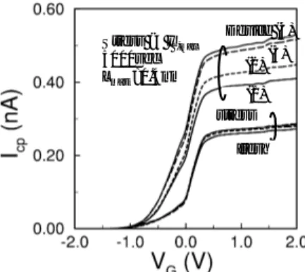
在本計劃中,乃以 NMOSFET 元件為 對象,以電漿蝕刻傷害的研究為目標,分 別進行以下三項之研究:(1)電漿傷害之基 本電性分析;(2) 四階段的電漿蝕刻傷害 機制;(3)電漿蝕刻傷害製程之改善等研 究。各項研究工作細節分述如下: (1) 電漿蝕刻傷害之基本電性分析 A. 與晶圓位置有關的電漿蝕刻傷害 首先,我們針對電漿蝕刻傷害之研究 設 計 出 四 種 不 同 天 線 結 構 的 佈 線 圖 案 (layout),分別如 Fig. 1 所示。其中,元件 (1)為標準元件﹔元件(2)為具有大面積天 線結構之待測元件﹔元件(3)為具有較疏 的梳狀(或指叉狀)天線結構﹔元件(4)為具 有較密的梳狀(或指叉狀)天線結構。其 中,元件(1)、(2)可用於研究天線面積大小 對電漿傷害之影響﹔元件(1)、(3)和(4)可用 於研究天線疏密對電漿傷害之影響。 其次,我們用基本 CP 法量得不同晶 圓位置下之電漿傷害結果,如 Fig. 2 所 示。在左圖中,乃是針對元件(1)所量測出 來的結果。其中,Icp電流量值可以直接反 映電漿蝕刻傷害之大小。在初始(fresh)狀 態時,NMOSFET 在晶圓(wafer)中心與邊 緣區域傷害量值大致上差不多﹔然而,經 過一段時間之熱載子加速測試(hot carrier stress)後,可以發現靠近晶圓邊緣區域的 元件其傷害明顯大於中心區域之元件。由 此可知,當元件在經過熱載子加速實驗之 後,電漿蝕刻傷害已經被突顯出來,而更 容易被觀測。接著,右圖,所得之結果類 似於左圖,只是電漿蝕刻傷害的量比左圖 來的大。這主要是因為元件(4)具有較大的 電漿蝕刻傷害,以致於 Icp電流在熱載子加 速實驗後明顯比元件(1)來的大許多。 由此可知,電漿蝕刻時會產生不均勻 的電漿電位分佈,以致於在晶圓表面的各 個區域會有不同程度之電漿蝕刻傷害。 B. 與天線結構有關之電漿蝕刻傷害 所謂天線結構指的乃是在電漿蝕刻製 程中,會收集/累積電漿電荷的結構或圖案 (例如電容結構、金屬佈線、多晶矽閘極 等) ,而後會將所收集之電漿電荷釋放而 對元件閘氧化層造成嚴重影響。隨著不同 電路的佈局,則會有不同的天線結構,這 將引發不同程度之電漿蝕刻傷害。 我們分別針對四種不同天線結構進行 電漿蝕刻傷害之測試,結果如 Fig. 3 所 示。由此可看出,在初始狀態時電漿傷害 的量值大致上仍是差不多﹔然而,經過一 段時間的熱載子加速實驗之後,即可以發 現電漿蝕刻傷害有在呈現出來。而電漿蝕 刻傷害程度依次為: 元件(4) > 元件(3) > 元件(2) > 元件(1)。 為何電漿蝕刻傷害在初始狀態下不會 顯現,然而在熱載子加速實驗之後又會再 被突顯出來呢? 主要可歸因於-在製程中 採 用 了 閘 極 再 氧 化 (poly-reoxidation) 製 程,大部分的製程傷害已被修補﹔然而, 當元件進行熱載子加速實驗時,這些被修 補過的區域卻是容易再次受傷,而再度反 映出電漿蝕刻傷害。 再者,由圖中可以看出元件(4)的傷害 最 大 , 這 因 為 它 具 有 最 大 的 天 線 週 長 (antenna peripheral length, APL)以及最大 的電子遮蔽效應(electron shading effect) (註: 電子遮蔽效應- 電漿蝕刻時,若是天 線密度過高,質量小的電子容易被散射到 其他區域﹔而質量大的帶正電電漿離子則 較易到達晶圓表面,以致於晶圓會累積大 量正電荷),所以電漿電荷收集量最大,電 漿蝕刻傷害也最大。其中,元件(2)雖擁有 最大的天線面積,但電漿電荷收集能力比 元件(4)小,所以整體電漿傷害還是較小。 以 往 的 研 究 認 為 天 線 效 應 (antenna effect)(或是電漿充放電傷害)與熱載子效 應無太大的關聯性。然而,由 Figs. 2 與 3 卻發現,電漿充放電傷害會導致元件熱載 子傷害上升。這可用後續的四階段電漿蝕 刻傷害機制來解釋,所以在這邊暫不論述。
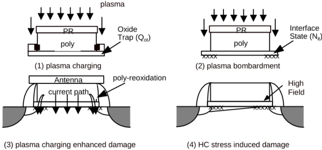
C. 與通道長度有關之電漿蝕刻傷害 當元件越做越小,電漿蝕刻傷害會對 元件造成不同程度的電漿蝕刻傷害。Fig. 4 所示乃是針對三種不同通道長度所量測之 電漿蝕刻傷害。Fig. 4(a)可以發現,在初始 狀態時,不管通道長短四種天線結構造成 的傷害量值大致上差不多﹔而經過熱載子 加速實驗之後,電漿蝕刻傷害已經變得很 明顯。同時可以發現元件通道長度為 0.6 微米時,Icp 電流曲線圖有彎折的情況發 生。 為了研究前述的彎折的現象,我們利 用 Icp的量測值去計算 Stress 前後產生的傷 害量(由於採用 IB,max stress,在這大部分將 產生界面的缺陷(interface state, Nit),結果 如 Fig. 4(b))。四種元件中對於長通道元件 所量測出來的傷害量大致上是差不多的﹔ 相對的,對於短通道元件量測出來之結 果,可以明顯的發現傷害量值隨著天線效 應(或是電漿充放電傷害)變大而變大。 由此可知,在這裡存在了兩個效應: 對長通道元件而言,電漿蝕刻傷害較不明 顯,所以熱載子效應主導元件的退化﹔對 短通道元件而言,電漿蝕刻傷害已經具有 主導的地位,所以電漿蝕刻傷害將主導元 件的退化。當這些傷害量反應到元件時, 可得到如 Fig. 5 的結果。在 Fig. 5(a)中,隨 著通道縮短,一方面熱載子效應已經變 大,一方面電漿蝕刻傷害也變明顯。在 Fig. 5(b)中,為了排除熱載子效應的部分(把元 件(1)當成參考),扣除這個分量,所得電漿 傷害的量隨著通道長度縮短而變大。 (2) 四階段的電漿蝕刻傷害機制 A. 四階段電漿蝕刻傷害之物理機制 為了更合理的解釋電漿蝕刻傷害機 制,在這我們提出一個“四階段的電漿蝕刻 傷害機制”,分別如 Fig. 6 所示。 在第一階段中,電漿蝕刻開始進行的 時候,天線結構(在這指 poly-Si gate)將會 收集大量電漿電荷,並累積電荷。等到電 荷累積到足夠產生 FN 穿隧效應之時,它 會以 FN 穿隧電流的形式流過閘極氧化 層。它的傷害類型類似於 FN stress,會產 生閘氧化層電荷缺陷(oxide trap),而現今 之研究稱此為“電漿充放電傷害”。 在第二階段中,當元件受到電漿離子 直接轟擊矽晶表面或是化學蝕刻劑與矽晶 表面起反應,它會造成矽晶表面或是閘氧 化 層 表 面 的 缺 陷 , 主 要 形 成 界 面 狀 態 (interface state),此即為電漿邊緣傷害。在 製程上,為了消瀰這些電漿蝕刻傷害,所 以進行閘極再氧化(poly-reoxidation)去降 低電漿蝕刻傷害,這可以消除大部分的閘 極邊緣區域的 Si-O 斷鍵。 到了第三階段,電漿電荷仍會繼續被 天線結構(此時指的乃是金屬佈線、電容等 結構)所收集。同樣的,累積電荷之後仍會 往下注入。然而,這時候前兩階段造成的 閘氧化層較弱的區域,具有較低的氧化層 屏障(oxide barrier),將會是排放此 FN 穿 隧電流的最佳路徑。而後,FN 電流流過 的結果,將再次的傷害這個較弱的閘氧化 層位置,造成嚴重的傷害。所以,在這吾 人稱之為「電漿充放電導致邊緣傷害」 (plasma charging enhanced edge damage, PCEED)。而此一現象,乃是吾人所首次發 表之新電漿蝕刻傷害現象。 最後到了第四階段,所生產之晶圓上 之電路將被操作於各種額定偏壓。我們用 熱載子加速測試來模擬這種操作下的傷害 情形。其中,在此加速測試中,靠近汲極 的區域將承受較大的電場,發生最大的衝 撞游離(impact ionization)﹔而且,在這個 汲極的附近,已有先前潛在性的電漿蝕刻 傷害,所以會再加劇元件可靠性的問題。 這四個階段的電漿蝕刻傷害會對元件 造成莫大的影響。其中,第三階段乃是我 們所首次發現的新現象,它特別會在短通 道元件中突顯出來,而嚴重影響元件電
性。而第四階段,雖然傳統上不歸類於電 漿蝕刻傷害,但它卻會被電漿蝕刻傷害所 大幅度的增強,所以在這亦列入考慮。 B. 以電荷幫浦分佈法驗證四階段電漿蝕 刻傷害機制 為了更深入的研究電漿蝕刻傷害發生 的機制,在這我們採用了電荷幫浦分佈 法。首先,我們透過量測元件在初始狀態 下的 Icp量值,得到 Fig. 7(a)。利用元件(1) 與(4)的 Icp 可以計算得到電漿充放電導致 的邊緣傷害,結果如 Fig. 7(b)所示。由本 圖可發現,此種電漿蝕刻傷害發生的位置 果然在靠近閘極邊緣的位置,跟前面理論 推估之位置相當接近。 當經過熱載子加速實驗之後,我們量 測 Icp量值,得到 Fig. 7(c)。分別利用 Stress 前後的 Icp 電流值計算傷害分佈情形,如 Fig. 7(d)之結果。在這裡,可以發現有兩個 峰值(peak)的傷害(界面狀態,Nit)分佈。其 中較大的 peak 位置與前述之電漿蝕刻導 致邊緣傷害(PCEED)之位置相同,由此推 斷這個傷害乃是由電漿蝕刻製程所造成 的。而第二個 peak 較小,我們認為是傳統 的熱載子傷害所造成的。為了證實這個想 法,我們利用 2D 的元件模擬計算出最大 電場的位置,也就是熱載子傷害最大的位 置,結果如 Fig. 8 所示,可以看出第二個 峰值位置與最大電場位置的確是吻合的。 由本研究可知,電漿充放電導致邊緣 傷害(PCEED)將主導元件的可靠性,且其 傷害量值將大於傳統熱載子傷害。所以, 在電漿蝕刻製程時,必須更慎重的防範電 漿蝕刻傷害之形成。 (3)電漿蝕刻傷害製程之改善研究 本研究最後的階段,我們利用三種不 同的方法來有效的降低電漿蝕刻傷害。分 別針對: (1)閘極氧化層品質- 此乃利用氮 化製程,針對閘極氧化層及通道位置進行 整體之改善;(2)閘極再氧化製程- 此乃利 用氮化製程,針對閘極邊緣區域進行傷害 修補﹔(3)控制電漿製程蝕刻時間- 採用較 短的時間去降低電漿蝕刻傷害。實驗量測 出來的結果,如 Fig. 9 所示。 對於初始狀態的電漿蝕刻傷害,可以 發現大致上改善的情況並不明顯,但仍可 看出降低電漿蝕刻時間最為有效降低電漿 蝕刻傷害的方法。然而,經過熱載子加速 測試的結果,得到的卻是經過氮化處理之 閘極再氧化製程最為有效的改善後續的可 靠性問題。 我們分析其結果,可把原因歸究於-由於電漿放電導致邊緣傷害(PCEED)乃是 發生於閘極邊緣區域的位置,針對這個區 域進行傷害之修補可以得到最有效之傷害 控制。 四、計劃成果自評 本 研 究 成 功 的 利 用 電 荷 幫 浦 分 佈 法研究電漿蝕刻傷害,除了推演出一套 完 整 的 四 階 段 電 漿 蝕 刻 傷 害 之 物 理 機 制,並分別利用三種不同的傷害改善製 程有效的降低電漿蝕刻傷害。 本計劃之完成,在學術界將可突破傳 統開創一個嶄新的研究方法,並領先國內 外電漿蝕刻傷害之研究。目前的研究成果 已有四篇國際性的會議論文,分別為一篇 IRPS(美國)[11]、一篇 SSDM(日本)[12]、 一 篇 IEDMS( 台 灣 )[13] 、 以 及 一 篇 VLSI-TSA(台灣)[14]。另外,更完整的研 究報告目前已經彙整完成,近期將投稿到 國際最大的期刊 IEEE T-ED 和 JJAP 等。 本計劃之進行,同時可以培養國內博、碩 士生在此領域之研究人才,並增進半導體 科技上之研究潛力。而在工業界,可廣泛 的使用於電漿蝕刻製程中,不管是量測或 是電漿蝕刻傷害製程的改善,皆有實際的 成效。既可改善良率又可降低其生產成 本。所以,本計劃的完成,將對學術界及 工業界研究水準的提昇有莫大的助益。
五、參考文獻
[1] X. -Y. Li et al., IEEE Proc. Int. Reliability Phys. Symp., p. 260, 1995.
[2] S. Krishnan et al, in Tech. Digest of International Electron Device Meeting (IEDM), p. 445, 1997.
[3] H. Shiu et al., IEEE Trans. Semicon. Manufacturing,
Vol. 6, No. 2, p. 96, 1993.
[4] Z. J. Ma et al., IEEE Electron Device lett., vol. 15,
No. 6. p. 224, 1994.
[5] T. Gu et al., IEEE Electron Device lett., Vol. 15, p.
48, 1994.
[6] M. G. El Hassan et al., IEEE Trans. Electron Devices,
Vol. 45, No. 4, p. 861, 1998.
[7] T. Brozek et al., IEEE Trans. Semicon. Manufacturing, Vol. 11, No. 2, p. 211, 1998.
[8] S. S. Chung et al., Proc. International Solid State Devices and Materials (SSDM), Chiba, Japan, p. 841,
1993.
[9] S. S. Chung et al., IEEE Trans. Electron Devices,
Vol. 46, No. 7, p. 1371, 1999.
[10] S. S. Chung et al., Proceedings of 1999 International Reliability Physics Symposium (IRPS), pp. 249-252,
March 22-25, San Diego, 1999.
[11] S. S. Chung et al., Proceedings of 2000 International Reliability Physics Symposium (IRPS), pp. 389-393,
Apr. 10-13, San Jose, 2000.
[12] S.-J. Chen et al., Proc. International Solid State Devices and Materials (SSDM),, pp. 16-17, Aug.
29-31, Sendai, 2000.
[13] S. J. Chen et al.,International Electron Devices and Materials Symposium (IEDMS), pp. 19-22, Dec.
20-22, 2000.
[14] S. J. Chen et al., in Proceedings of Symp. VLSI-TSA,
April 18-20, Hsinchu, Taiwan, 2001.
Device (4) (1) (3) (2) stress fresh Stress @ IB,max 5000sec Lmask=0.4µm
Fig. 3 Charge pumping measurement for four kinds of antenna structures. Although the plasma damage were eliminated in the poly-reoxidation process (fresh), much more interface trap has been re-introduced after HC stress.
Stress @ IB,max 5000sec Lmask= 0.4µm Device (4) Device (1) stress stress fresh fresh (4) (3) (1) D B G S (2) Antenna
Fig. 5 Length dependence of the drain current degradation (a) and the etch-pattern enhanced damage effect (b). Short channel device shows enhanced drain current degradation by
comparing with long channel ones. Fig. 2 Charge pumping measurement for devices (1) and (4)
at the wafer edge and the center. At the edge, device degradation is enhanced after HC stress, especially for device (4).
Fig. 1 Four kinds of antenna structures used in this study. Device (1): control sample; Device (2): with large-area antenna; Device (3): with low-density comb-like antenna; Device (4): with high-density comb-like antenna.
Fig. 4 Length dependence of maximum charge pumping current (a) and Nit(b). Short channel devices have large∆Icp
for four kinds of structures than long channel ones. Larger interface traps are as a result of plasma edge damage.
(4) (3) (2) (1) (4) (3) (2) (1) Stress Fresh (a) (b) Icp,max= qfNitWL (4) (3) (2) (1) (a) (b) (4) - (1) (3) – (1) (2) – (1) (1 )
(a) (c) device (4) fresh devices CP currents stress device (1) Icp,(4)-Icp,(1) to extract Nit fresh device (1)(4) fresh & stress devices CP currents Icp,stress-Icp,fresh
to extract Nit
(b)
(d)
plasma charging enhanced edge damage
plasma charging enhanced
HC effect device (4) (1) due to max. field (1) plasma charging plasma Oxide Trap (Qot) PR poly (2) plasma bombardment Interface State (Nit) PR poly xxxx xxxx Antenna current path poly-reoxidation xxxx xxxx
(3) plasma charging enhanced damage (4) HC stress induced damage
High Field xxxx xxxxxx Simulation@atlas Bias: VDS = 3.3V VGS= 1.4V Drain Source Gate Bulk 0.1 0.2 0.3 0.4 0.30µm A A* B B* C C* (max. field)
Fig. 6 Four phases inducing the plasma damage: (1) plasma charging; (2) plasma bombardment; (3) plasma charging enhanced damage; (4) HC stress induced damage.
Fig. 7 (a) and (b) Icp and Nit for plasma charging enhanced edge damage. (c) and (d) Icpand Nitdue to plasma charging enhanced HC effect. Note that 2 peaks of Nitare observed.
Fig. 8 Simulated electric field for device under HC (@IB,max) stress.
O2 N2O conv. improved 40 sec 20 sec gate oxide poly reox. O2 etch time N2O stress fresh gate oxide poly reoxidation etch time
Fig. 9 Three curing processes to suppress the plasma induced damage.