國 立 交 通 大 學
奈 米 科 技 研 究 所
碩 士 論 文
單晶矽應用於軟性電子元件之研究
Single crystal silicon for the
flexible electronic device applications
研 究 生:林京璋
指導教授:柯富祥教授
單晶矽應用於軟性電子元件之研究
Single crystal silicon for the
flexible electronic device applications
研究生:林京璋 Student:Ching-Channg Lin
指導教授:柯富祥 Advisor:Dr. Fu-Hsiang Ko
國 立 交 通 大 學
奈 米 科 技 研 究 所
碩 士 論 文
A ThesisSubmitted to Institute of Nanotechnology College of Engineering
National Chiao Tung University in partial Fulfillment of the Requirements
for the Degree of Master in
Institute of Nanotechnology April 2009
Hsinchu 300, Taiwan
i
Acknowledgment
本研究之得以順利完成,首先感謝恩師 柯富祥教授這兩年來對
學生不論是在學問研究方面及待人處世上的指導與教誨,以及對於研
究內容及成果,均悉心校閱與指正,師恩浩瀚,學生銘感於心。另外,
在研究期間承蒙俊淇學長這一路上的帶領,從一開始完全在狀況外的
我,到現在能夠將論文完成,對本研究提供諸多寶貴意見,使得論文
更佳紮實,於此謹致誠摯謝意。
在研究所這兩年生活中,特別感謝其昌學長、佳典學長、銘清學
長、美榕學姐、志杰學長、德玲學姊、中書學長、依蓁學姐的指導與
照顧,教導我實驗室的生態與做人處事的道理,從學長姐們的身上學
到許多書本中沒學過的事物,讓我受益良多。還有一路走來的同窗好
友們鄭捷、玟菲、嘉琦的相互扶持與勉勵;以及戰友柏軒常常聽我在
抱怨並適時的給我建議,常賦予生活上以及精神上的一劑強心針,在
此致以無限的謝意。也感謝學弟學妹們在實驗研究上的協助與幫忙。
最後我要感謝一路支持我的家人—因為有爸爸媽媽的支持,兩個
弟弟的關心及激勵,我才可以完成碩士學業,願將所有成就與你們分
享。
ii
單晶矽應用於軟性電子元件之研究
學生: 林京璋 指導教授: 柯富祥
國立交通大學
奈米科技研究所
碩士論文初稿
摘 要
近年來,隨著科技的日益進步,以及眾多的需求上,使得軟性電
子元件最近成為矚目的焦點。軟性電子元件能夠讓元件具有彈性及可
撓曲性,並使其能夠使用並貼附在各種曲面上,讓各種原件的應用性
大幅提升。
傳統上軟性電子元件使用有機或非晶矽過程製造,並使用塑膠基
板,但非晶矽電子元件的電性相較於一般不可撓的單晶矽基材元件為
差,且塑膠基板不能耐高溫無法使用一般工業化製成。若能開發軟性
單晶矽元件不使用塑膠基板並兼容於現有製程,將能大大的提高了軟
iii
性電子元件的實用性且提供更佳的電子性質。
本研究中將使用單晶矽做為基材,使用化學蝕刻技術將單晶矽蝕
刻至可撓曲的厚度以取代塑膠基板,整合單晶矽製程製造元件,提供
簡單的製程步驟製作出高性能的軟性電子元件。此研究結果將能應用
於隨身攜帶之電子產品及生醫感測元件等等會讓元件產生形變並需
要極佳靈敏度的元件使用上。
iv
Single crystal silicon for the
flexible electronic device applications
Student:Ching-Chang Lin Advisor:Dr. Fu-Hsiang Ko
Institute of Nanotechnology
National Chiao Tung University
ABSTRACT
Recently, scientists have focused on the flexible technology for the needs of flexibility and elasticity. Flexible technology makes electronic devices flexible enough to fit on a curved surface perfectly and can be applied in a variety of applications.
Organics, amorphous silicon and plastic substrates used in traditional flexible devices have rather poor electrical properties. Moreover, the plastic substrates can’t withstand the high temperature in industrial procedure. The highly electrical properties can be achieved if it is possible to develop single crystal silicon devices instead of plastic substrate and compatible the flexible silicon with general procedure.
In this study, the single crystal silicon wafers are choosed as substrates. The wafers undergo a chemical etching process to approach ultrathin single crystal silicon chips. In addition, we manufacture high quality flexible devices through integrated
v
devices-fabricating process. And the resultant devices are utilized to mobile electronic products and biomedical applications.
vi
Contents
Acknowledgment………....……….i
Abstract (Chinese) ……….…...………..ii
Abstract (English) ……….………....…iv
Contents………...………...……….vi
List of tables………...………...………...viii
List of Figures ………..………..ix
Chapter 1: Introduction………...………...……….…....1
1.1 General Introduction……….………..……..………..…...1
1.2 Introduction of Flexible Electronics………..…….…1
1.3 Introduction of Silicon………..…...3
1.3-1 Single Crystal silicon………5
Chapter 2: Principles and Operations ……..……….……….…...8
2.1 General flexible electronics………..………..…8
2.2 Wet Etching………..…9 2.3 Electronic Devices……….……….………10 2.3-1 MSM Photodetector…...10 2.3-2 PN Diode…...11 2.3-3 NPN Transistor.………….………….………12 2.3-4 Solar Cell………..………...13
2.4 Texturisation of the Pyramidal Structure...14
2.5 Motivation……….……….15
vii
Chapter 3: Experimental ……….…...17
3.1 The Etching Process by NaOH…...17
3.2 The Texturing Process by TMAH…...18
3.3 MSM Photodetector Process……….….………26
3.4 PN Diode Process……….………..27
3.5 NPN Transistor Process……...……...……….………..27
3.6 Solar Cell Process………..….………28
Chapter 4: Results and Discussion ………….…….……….…...30
4.1 The Silicon Thin Chip by Etching……….………30
4.2 Optimal Conditions of Anisotropic Texturisation….………35
4.2-1 Surface Morphology of the Pyramidal Structure and Its Reflectivity Analysis……….…….………35
4.2-2 Surface Energy of the Pyramidal Structure…….………41
4.3 Electrical Properties of flexible devices…….………44
4.3-1 Electrical Properties of MSM Photodetector…….…….………44
4.3-2 Electrical Properties of PN Diode….….….………49
4.3-3 Electrical Properties of NPN Transistor……..………53
4.3-4 Electrical Properties of Solar Cell…….……….……….54
Chapter 5: Conclusions……….……….………...59
viii
List of Tables
Chapter 1
Table 1-1 Properties of different flexible plastic substrates………….……….3 Table 1-2 Compare the electron and hole mobilities of amorphous and crystalline silicon………...………….7
Chapter 4
Table 4-1 The measurement of contact angle with different etching time by 1.19 %
TMAH and 50 % of IPA solution at 80 0C……..………….………43
Table 4-2 The measurement of surface tension and total surface energy with different
ix
List of Figures
Chapter 2
Figure 2-1 The figure shows different mobilities between types of silicon and organic maerials.……….………..8 Figure 2-2 The overall flow of this study……….…16
Chapter 3
Figure 3-1 The vertical etching installation……….17 Figure 3-2 The morphology of silicon anisotropic etched in 2.38 % TMAH solution at 60 °C for 60 min. (a) shows the AFM morphology in 10 μm × 10 μm area, and (b) shows the SEM morphology. ………19 Figure 3-3 The morphology of silicon anisotropic etched in 2.38 % TMAH solution at 70 °C for 60 min. (a) shows the AFM morphology in 10 μm × 10 μm area, and (b) shows the SEM morphology.……….19 Figure 3-4 The morphology of silicon anisotropic etched in 2.38 % TMAH solution at 80°C 60 min. (a) shows the AFM morphology in 10 μm × 10 μm area, and (b) shows the SEM morphology.………20 Figure 3-5 The reaction of general texturing silicon surface………...…20 Figure 3-6 The morphology of silicon anisotropic etched in 1.67 % TMAH and 30 % IPA at 60 °C for 60 min. (a) shows the AFM morphology in 10 μm × 10 μm area, and (b) shows the SEM morphology.………..…...21
x
Figure 3-7 The morphology of silicon anisotropic etched in 1.67 % TMAH and 30 % IPA solution at 70 °C for 60 min. (a) shows the AFM morphology in 10 μm × 10 μm area, and (b) shows the SEM morphology………21 Figure 3-8 The morphology of silicon anisotropic etched in 1.67 % TMAH and 30 % IPA solution at 80 °C for 60 min. (a) shows the AFM morphology in 10 μm × 10 μm area, and (b) shows the SEM morphology.………22 Figure 3-9 The relationship of the average height of the etched silicon as a function of temperature.……….……….……….22 Figure 3-10 The AFM and SEM morphology of etched silicon etched by TMAH and IPA with different concentrations at 80 °C for 60 min. The concentrations of TMAH and IPA are 1.67 % and 30 % respectively in (a) (b), 1.19 % and 50 % respectively in (c) (d) and 0.714 % and 70 % in (e) and (f)………..………24 Figure 3-11 The resulting height of pyramidal structure etched in different concentration of TMAH and IPA at 80 °C………25 Figure 3-12 The manufacturing process of MSM photodetectors and PN diodes...…26 Figure 3-13 The manufacturing process of NPN transistors………26 Figure 3-14 The manufactuing process of solar cells………28
Chapter 4
Figure 4-1 The ultrathin silicon chips after etching. (a) optical image of 30μ m-thick silicon chip (b) optical image of 30μ m-thick silicon chip with electrode film……….………30 Figure 4-2 The croess-section SEM image of the 30μ m-thick ultrathin silicon chip……….….…31
xi
Figure 4-3 X-Ray diffraction measurement of ultrathin silicon chips. (a) The database of silicon. (b) X-Ray diffraction diagram of bulk 675μ m-thick silicon wafer. (c) X-Ray diffraction diagram of ultrathin 30μ m-thick silicon chip……… .……33 Figure 4-4 The Hall mobility of ultrathin silicon chip is 773 cm2/V-S……….34 Figure 4-5 The AFM and SEM texturing morphology of silicon wafers etched in 1.19 % of TMAH and 50 % of IPA at 80 °C with varying time. (a) and (b) are the morphology of silicon wafers textured for 30 min; the texturing time is 60 min for (c) and (d); 90 min for (e) and (f); and 120 min for (g) and (h)………..….…………..36 Figure 4-6 Average height of pyramidal structures with different etching time. The
highest density and optimal pyramids result from the 120 min processing time, and the average height is 3.01 μm………...………..…37 Figure 4-7 Comparison of the reflectivity of silicon surface with pyramidal structures during with different texturing time.………..……..………40 Figure 4-8 The reflectivity of silicon substrate with and without texturization process by N&K analyzer. The reflectivity of TMAH-textured silicon substrate wi t h a t hi n gol d film i s down t o 2.00 % at 400 nm li ght wavelength…….……….……….…………..40 Figure 4-9 The drop of DI water on the gold thin film coating on the textured surface. The contact angle of water droplet and film is 30.2 degree which means the hydrophilic feature of optimal texturing substrate etched on the conditions of 1.19 % TMAH and 50 % of IPA solution at 80 0C for 120 min………...……….…………42 Figure 4-10 Power intensity of halogen lamp measured by calibration photodiode………45
xii
Figure 4-11 The I-V characteristic of MSM photodetector with interdigitated lines………..………46 Figure 4-12 The dark and light I-V characteristic of MSM photodetector with interdigitated lines………..46 Figure 4-13 The durability of MSM photodetector.……….………47 Figure 4-14 The dark and light I-V characteristic of MSM photodetector bent with various curvature radius.………..…………48 Figure 4-15 The difference I-V characteristic of MSM photodetector between unbending and bent for 100 times……….…..………48 Figure 4-16 The I-V characteristic of PN diode.……….………49 Figure 4-17 The dark and light I-V characteristic of PN diode.……….…….………50 Figure 4-18 The durability of PN diode.……….……51 Figure 4-19 The dark and light I-V characteristic of PN diode bent with various curvature radius.………..………51 Figure 4-20 The difference I-V characteristic of PN diode between unbending and been for 100 times……….……….52 Figure 4-21 Time mode electrical steady test for MSM photodetector and PN diode.………..52 Figure 4-22 The I-V characteristic of NPN transistor in log scale.……….…………53 Figure 4-23 The I-V characteristic of NPN transistor in linear scale.……….………54 Figure 4-24 The I-V characteristic of solar cell in linear scale (-10 V~5V)..………..55 Figure 4-25 Figure 4-25 I-V characteristic of solar cell in linear scale (0V~0.12V)………..…………....55 Figure 4-26 The durability of solar cell..………...………..……….…56 Figure 4-27 The dark and light I-V characteristic of solar cell bent with various curvature radius………..…57
xiii
Figure 4-28 Time mode electrical steady test for solar cell……….57 Figure 4-29 Optical images of flexible solar cells with conductive copper adhesive tape………..……….58
1
Chapter 1 Introduction
1.1 General Introduction
Electronic devices with performance equal to established technologies that use rigid semiconductor wafers, but in lightweight, flexible formats would enable many new applications. Examples include wearable systems for personal health monitoring and therapeutics, “smart” surgical gloves with integrated electronics, and electronic eye–type imagers that incorporate focal plane arrays on hemispherical substrates [1-3]. Circuits that use organic [4-5] or certain classes of inorganic [6 -13] electronic materials on plastic or steel foil substrates can provide some degree of mechanical flexibility, but they cannot be folded. Also, with few exceptions [11-13] such systems offer only modest electrical performance. Flexible metal interconnects with rigid [14] or flexible inorganic device [15-17] components represent alternative strategies that can also, in certain cases, provide high performance. In their existing forms, however, none of these approaches allows scaling to circuit systems with practically useful levels of functionality.
1.2 Introduction of Flexible Electronics
Flexible electronics [18-20], also known as flexible circuits or flexible circuit boards, is a technology for assembling electronic circuits by mounting electronic devices on flexible high-performance plastic substrates [21], such as polyimide film. Additionally, flex circuits can be screen printed silver circuits on polyester [22-29]. Flexible electronic assemblies may be manufactured using identical components used for rigid printed circuit boards, allowing the board to conform to a desired shape, or to
2
flex during its use. Flexible substrates have several advantages in many applications: • Tightly assembled electronic packages, where electrical connections are required
in 3 axis, such as cameras (static application).
• Electrical connections where the assembly is required to flex during its normal use, such as folding cell phones (dynamic application).
• Electrical connections between sub-assemblies to replace wire harnesses, which are heavier and bulkier, such as in rockets and satellites.
• Electrical connections where board thickness or space constraints are driving factors.
Flexible circuits are often used as connectors in various applications where flexibility, space savings, or production constraints limit the serviceability of rigid circuit boards or hand wiring. In addition to cameras, a common application of flex circuits is in computer keyboard manufacturing; most keyboards made today use flex circuits for the switch matrix.
• In LCD fabrication, glass is used as a substrate. If thin flexible plastic or metal foil is used as the substrate instead, the entire system can be flexible, as the film deposited on top of the substrate is usually very thin, on the order of a few micrometers.
• OLEDs are normally used instead of a back-light for flexible displays, making a flexible organic light-emitting diode display.
• Flexible solar cells have been developed for powering satellites. These cells are lightweight, can be rolled up for launch, and are easily deployable, making them a good match for the application.
3
Table 1-1 The properties of different flexible plastic substrates.
1.3 Introduction of Silicon
Silicon is the most common metalloid. It is a chemical element, which has the symbol Si and atomic number 14. The atomic mass is 28.0855. A tetravalent metalloid, silicon is less reactive than its chemical analog carbon. As the eighth most common element in the universe by mass, silicon very rarely occurs as the pure free element in nature, but is more widely distributed in dusts, planetoids and planets as various forms of silicon dioxide (silica) or silicates. On Earth, silicon is the second most abundant element (after oxygen) in the crust [30], making up 25.7% of the crust by mass.
Silicon has many industrial uses. Elemental silicon is the principal component of most semiconductor devices, most importantly integrated circuits or microchips.
4
Silicon is widely used in semiconductors because it remains a semiconductor at higher temperatures than the semiconductor germanium and because its native oxide is easily grown in a furnace and forms a better semiconductor/dielectric interface than any other material.
In the form of silica and silicates, silicon forms useful glasses, cements, and ceramics. It is also a constituent of silicones, a class-name for various synthetic plastic substances made of silicon, oxygen, carbon and hydrogen, often confused with silicon itself. Silicon is an essential element in biology, although only tiny traces of it appear to be required by animals. It is much more important to the metabolism of plants, particularly many grasses, and silicic acid (a type of silica) forms the basis of the striking array of protective shells of the microscopic diatoms.
The outer electron orbitals (half filled subshell holding up to eight electrons) have the same structure as in carbon and the two elements are sometimes similar chemically. Even though it is a relatively inert element, silicon still reacts with halogens and dilute alkalis, but most acids (except for some hyper-reactive combinations of nitric acid and hydrofluoric acid) do not affect it. Having four bonding electrons however gives it, like carbon, many opportunities to combine with other elements or compounds under the right circumstances.
Both silicon and (in certain aspects) carbon are semiconductors, readily either donating or sharing their four outer electrons allowing many different forms of chemical bonding. Pure silicon has a negative temperature coefficient of resistance, since the number of free charge carriers increases with temperature. The electrical resistance of single crystal silicon significantly changes under the application of mechanical stress due to the piezoresistive effect. In its crystalline form, pure silicon has a gray color and a metallic luster. It is similar to glass in that it is rather strong, very brittle, and prone to chipping.
5
As the second most abundant element in the earth's crust, silicon is vital to the construction industry as a principal constituent of natural stone, glass, concrete and cement. Silicon's greatest impact on the modern world's economy and lifestyle has resulted from silicon wafers used as substrates in the manufacture of discrete electronic devices such as power transistors, and in the development of integrated circuits such as computer chips.
Pure silicon is used to produce ultra-pure silicon wafers used in the semiconductor industry, in electronics and in photovoltaic applications. Ultra-pure silicon can be doped with other elements to adjust its electrical response by controlling the number and charge (positive or negative) of current carriers. Such control is necessary for transistors, solar cells, integrated circuits, microprocessors, semiconductor detectors and other semiconductor devices which are used in electronics and other high-tech applications. In Photonics, silicon can be used as a continuous wave Raman laser medium to produce coherent light, though it is ineffective as a light source. Hydrogenated amorphous silicon is used in the production of low-cost, large-area electronics in applications such as LCDs, and of large-area, low-cost thin-film solar cells.
1.3-1 Single Crystal Silicon
Silicon, like carbon and other group IV elements form face-centered diamond cubic crystal structure. Silicon, in particular, forms a face-centered cubic structure with a lattice spacing of 5.430710 Å (0.5430710 nm) [31]. The majority of silicon crystals grown for device production are produced by the Czochralski process, (CZ-Si) since it is the cheapest method available and it is capable of producing large size crystals. However, silicon single-crystals grown by the Czochralski method contain
6
impurities since the crucible which contains the melt dissolves. For certain electronic devices, particularly those required for high power applications, silicon grown by the Czochralski method is not pure enough. For these applications, float-zone silicon (FZ-Si) can be used instead. It is worth mentioning though, in contrast with CZ-Si method in which the seed is dipped into the silicon melt and the growing crystal is pulled upward, the thin seed crystal in the FZ-Si method sustains the growing crystal as well as the polysilicon rod from the bottom. As a result, it is difficult to grow large size crystals using the float-zone method. Today, all the dislocation-free silicon crystals used in semiconductor industry with diameter 300 mm or larger are grown by the Czochralski method with purity level significantly improved.
Silicon is pulled as single crystal. The internal crystalline structure is completely homogenous, which can be recognized by an even external coloring.
Semiconductor grade (also solar grade) polycrystalline silicon is converted to "single crystal" silicon - meaning that the randomly associated atoms of silicon in "polycrystalline silicon" are converted to large "single" crystals of silicon. Single crystal silicon is used to manufacture 99% of all electronic devices. The devices are used in watches, refrigerators, microwaves, televisions, radios, communications equipment such as cell phones, and controls for cars, ships, aircraft, missiles, and atomic weapons.
A single crystal, also called monocrystal, is a crystalline solid in which the crystal lattice of the entire sample is continuous and unbroken to the edges of the sample, with no grain boundaries. The opposite of a single crystal sample is an amorphous structure where the atomic position is limited to short range order only. In between the two extremes exist polycrystalline and paracrystalline phases, which are made up of a number of smaller crystals known as crystallites. Because of a variety of entropic effects on the microstructure of solids, including the distorting effects of
7
impurities and the mobility of crystallographic defects and dislocations, single crystals of meaningful size are exceedingly rare in nature, and can also be difficult to produce in the laboratory under controlled conditions.
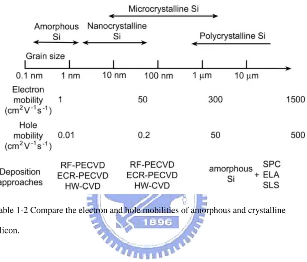
Table 1-2 Compare the electron and hole mobilities of amorphous and crystalline silicon.
8
Chapter 2 Principles and Operations
2.1 General flexible electronics
Flexible electronic devices with plastic substrates have been attracted interesting recently. Due to advantages of lighter, thinner, less unbreak, higher impact resistance and can be scaled up for roll-to-roll process technology, plastic substrate has been considered to be a promise candidate for flexible electronic device application. To replace rigid substrate, however, several physics properties need to be concerned, such as dimensional stability, thermal stability and low coefficient of thermal expansion (CET) and so on.
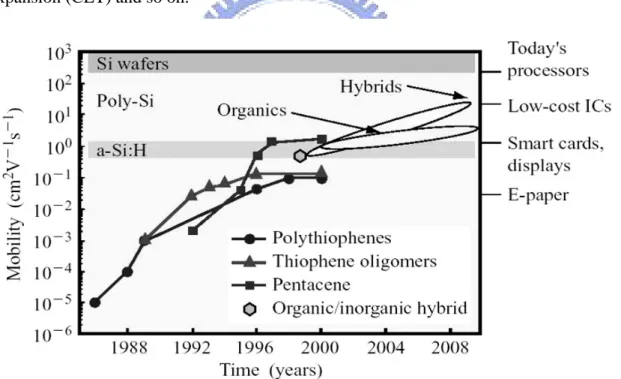
Figure 2-1 The figure shows different mobilities between types of silicon and organic materials.
9
2.2 Wet Etching
Etching is used in microfabrication to chemically remove layers from the surface of a wafer during manufacturing. Etching is a critically important process module, and every wafer undergoes many etching steps before it is complete.
For many etch steps, part of the wafer is protected from the etchant by a "masking" material which resists etching. In some cases, the masking material is photoresist which has been patterned using photolithography. Other situations require a more durable mask, such as silicon nitride.
The first etching processes used liquid-phase ("wet") etchants. The wafer can be immersed in a bath of etchant, which must be agitated to achieve good process control. For instance, buffered hydrofluoric acid (BHF) is used commonly to etch silicon dioxide over a silicon substrate.
Different specialised etchants can be used to characterise the surface etched. Wet etchants are usually isotropic, which leads to large bias when etching thick films. They also require the disposal of large amounts of toxic waste. For these reasons, they are seldom used in state-of-the-art processes. However, the photographic developer used for photoresist resembles wet etching.
As an alternative to immersion, single wafer machines use the Bernoulli principle to employ a gas (usually, pure nitrogen) to cushion and protect one side of the wafer while etchant is applied to the other side. It can be done to either the front side or back side. The etch chemistry is dispensed on the top side when in the machine and the bottom side is not affected. This etch method is particularly effective just before "backend" processing (BEOL), where wafers are normally very much thinner after wafer backgrinding, and very sensitive to thermal or mechanical stress. Etching a thin layer of even a few micrometres will remove microcracks produced
10
during backgrinding resulting in a wafer having dramatically increased strength and flexibility without breaking.
Some wet etchants etch crystalline materials at very different rates depending upon which crystal face is exposed. In single-crystal materials (e.g. silicon wafers), this effect can allow very high anisotropy.
Several anisotropic wet etchants are available for silicon. For instance, potassium hydroxide (KOH) can achieve selectivity of 400 between <100> and <111> planes. Another option is EDP (an aqueous solution of ethylene diamine and pyrocatechol), which also displays high selectivity for p-type doping. Neither of these etchants may be used on wafers that contain CMOS integrated circuits. Both of them etch aluminium, commonly used as a metallization (wiring) material. KOH introduces mobile potassium ions into silicon dioxide, and EDP is highly corrosive and carcinogenic. Tetramethylammonium hydroxide (TMAH) presents a safer alternative, although it has even worse selectivity between <100> and <111> planes in silicon than does EDP.
2.3 Electronic Devices
2.3-1 MSM Photodetector
Photodetectors are devices used for detection of light and converted electric signal from optical radiation with the source of visible, infrared, or ultraviolet wavelength. The important issues of these detectors are its signal to noise ratio, spatial resolution, ability to operate through a range of high to low input light levels, and spectral response. They are often used in sensing objects or encoding data by a change in transmitted or reflected light. There are many types of photodetectors which may
11
be appropriate in a particular case [32]:
A. Photodiode is a semiconductor device with p-n or p-i-n junction, where detects of light and generates a photocurrent. A particularly sensitive device is avalanche
photodiodes, which can potentially provide higher gain bandwidth performance. B. The metal-semiconductor-metal (MSM) photodetector is containing two
Schottky barrier contacts of doped semiconductor material. The MSM device can be used as a photodetector by shining light on the top surface of the structure. When light impinges the electrodes of the semiconductor, it generates electric carriers, and is collected by the electric field and thus can form a photocurrent. C. Phototransistor is similar to photodiode but relatively more complicated to
fabricate and generally require sizeable chip area. However, it is attractive for detection applications since it can achieve high gain through transistor action.
2.3-2 PN Diode
In electronics, a diode is a two-terminal device (thermionic diodes may also have one or two ancillary terminals for a heater). Diodes have two active electrodes between which the signal of interest may flow, and most are used for their unidirectional electric current property. The varicap diode is used as an electrically adjustable capacitor.
The unidirectionality most diodes exhibit is sometimes generically called the rectifying property. The most common function of a diode is to allow an electric current in one direction (called the forward biased condition) and to block the current in the opposite direction (the reverse biased condition). Thus, the diode can be thought of as an electronic version of a check valve.
12
complex non-linear electrical characteristic, which depends on the particular type of diode technology. Diodes also have many other functions in which they are not designed to operate in this on-off manner.
Early diodes included “cat’s whisker” crystals and vacuum tube devices (also called thermionic valves). Today the most common diodes are made from semiconductor materials such as silicon or germanium.
Most modern diodes are based on semiconductor p-n junctions. In a p-n diode, conventional current is from the p-type side (the anode) to the n-type side (the cathode), but not in the opposite direction. Another type of semiconductor diode, the Schottky diode, is formed from the contact between a metal and a semiconductor rather than by a p-n junction.
2.3-3 Transistor
In electronics, a transistor is a semiconductor device commonly used to amplify or switch electronic signals. A transistor is made of a solid piece of a semiconductor material, with at least three terminals for connection to an external circuit. A voltage or current applied to one pair of the transistor's terminals changes the current flowing through another pair of terminals. Because the controlled (output) power can be much larger than the controlling (input) power, the transistor provides amplification of a signal. The transistor is the fundamental building block of modern electronic devices, and is used in radio, telephone, computer and other electronic systems. Some transistors are packaged individually but most are found in integrated circuits.
The bipolar junction transistor, or BJT, was the first transistor invented, and through the 1970s, was the most commonly used transistor. Even after MOSFETs became available, the BJT remained the transistor of choice for many analog circuits
13
such as simple amplifiers because of their greater linearity and ease of manufacture. Desirable properties of MOSFETs, such as their utility in low-power devices, usually in the CMOS configuration, allowed them to capture nearly all market share for digital circuits; more recently MOSFETs have captured most analog and power applications as well, including modern clocked analog circuits, voltage regulators, amplifiers, power transmitters, motor drivers, etc.
2.3-4 solar cell
A solar cell or photovoltaic cell is a device that converts sunlight directly into electricity by the photovoltaic effect [33]. Sometimes the term solar cell is reserved for devices intended specifically to capture energy from sunlight, while the term photovoltaic cell is used when the light source is unspecified. Assemblies of cells are used to make solar panels, solar modules, or photovoltaic arrays. Photovoltaics is the field of technology and research related to the application of solar cells in producing electricity for practical use. The energy generated this way is an example of solar energy (also called solar power).
The most commonly known solar cell is configured as a large-area p-n junction made from silicon. As a simplification, one can imagine bringing a layer of n-type silicon into direct contact with a layer of p-type silicon. In practice, p-n junctions of silicon solar cells are not made in this way, but rather, by diffusing an n-type dopant into one side of a p-type wafer.
If a piece of p-type silicon is placed in intimate contact with a piece of n-type silicon, then a diffusion of electrons occurs from the region of high electron concentration (the n-type side of the junction) into the region of low electron concentration (p-type side of the junction). When the electrons diffuse across the p-n
14
junction, they recombine with holes on the p-type side. The diffusion of carriers does not happen indefinitely however, because of an electric field which is created by the imbalance of charge immediately on either side of the junction which this diffusion creates. The electric field established across the p-n junction creates a diode that promotes charge flow, known as drift current, that opposes and eventually balances out the diffusion of electron and holes. This region where electrons and holes have diffused across the junction is called the depletion region because it no longer contains any mobile charge carriers. It is also known as the "space charge region".
2.4 Texturisation of the Pyramidal Structure
There are lots of researches for random pyramidal texturing structures, due to decrease reflectivity of silicon solar cells and increase the short circuit current of the devices [34]. Anisotropic etching of silicon plays an important role for fabricating various three-dimensional structures such as thin membranes and silicon microbridges for solar cell systems and IC processing. The most commonly and simple way is using chemical etching solutions, NaOH or KOH. However, these chemical solutions containing K+ or Na+ ions are toxic, pollutant and the passivation layers (SiO
2 or SiN)
deposited on the surface of the cell are contaminated after texturisation. An alternative to texturisation is tetramethyl ammonium hydroxide (TMAH). It was found that TMAH is not pollutant, not toxic and its use leads also to good etching characteristics of a pyramidal structure [34-36]. Moreover, the etching rate and surface morphology can be controlled by the etching parameters, such as concentration of the solution, temperature and the addition of surfactant.
In this study, we investigate the etching process of silicon wafers with TMAH solutions of varying concentration under different temperature and surfactant
15
conditions. This experiment with texturing the silicon substrates can generate the pyramidal structures which provide that aims of increasing the surface areas and decreasing reflectivity. The appearance of increasing surface areas has better perform of the immobilization lipase on the surface compared to the substrate without pyramidal structures. When decreasing the reflectivity, it can convert light signal to electric signal more completely, which has the same characteristics with solar cell [37].
2.5 Motivation
Semiconductors based on organic small molecules and polymers provide a route to printed electronics on low temperature plastic substrates [38]. Although useful systems in areas such as displays can be achieved with these materials, the modest performance (i.e., device mobilities typically less than 1–2 cm2/V-S), which is currently possible may limit the range of applications. Some recent research that is designed to address this issue, while retaining the attractive processing attributes of the organics, explores the use of unusual structural forms—micro/nanowires, platelets, ribbons, etc.—of high quality single-crystal inorganic semiconductors [39-43]. There are two general techniques for generating the devices: one that uses direct guided growth
[43]
and another that applies lithographic and etching methods to wafer scale sources of a material [39-41]. The study approach is attractive because the quality of the material, its doping levels [44-47], etc., are all controlled by the well-known processes used to create the wafers.
16
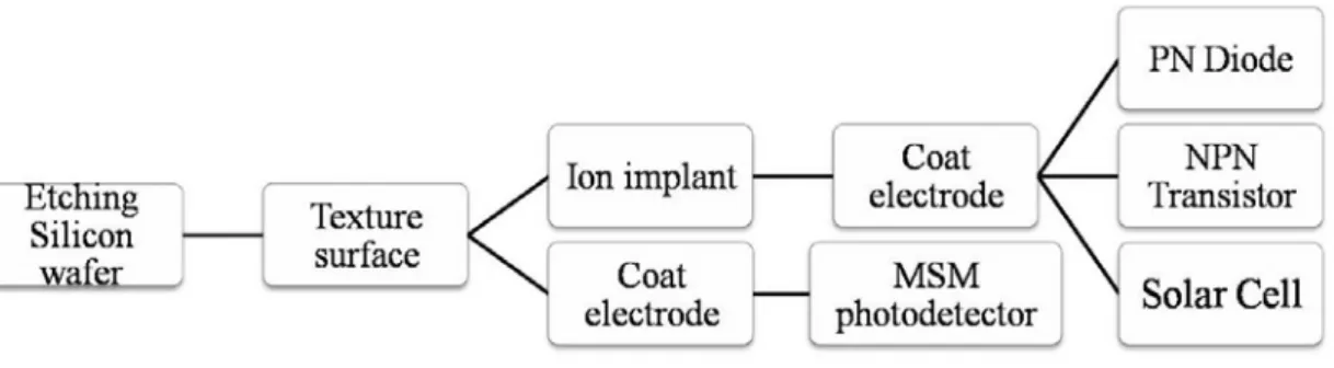
2.6 Thesis Organization
In this study, we report the single crystal silicon for the flexible electronic devices. Our experimental flow is shown in figure 2-2.
Figure 2-2 The overall flow of this study.
The thesis is divided into five chapters. In chapter 1 is the general overview of the background of this study. Literature surveys the fabrication of MSM photodetector, PN diode, NPN transistor, and solar cell. The principles and operations of this experiment are introduced in chapter 2. The detailed fabrication processes are presented in chapter 3. In chapter 4, we discuss the electrical performance and the anisotropic texturisation. Finally, we summarize the contribution of our research in chapter 5.
17
Chapter 3 Experimental
3.1 Wet Etching
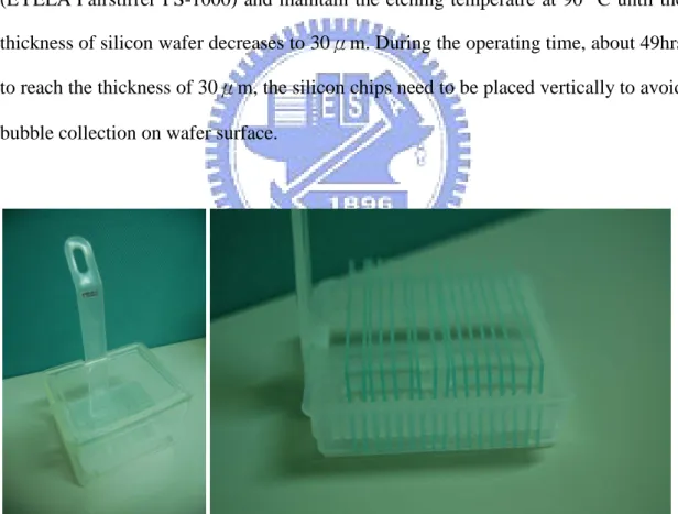
The process, which is built on our recent work in single-crystalline silicon for flexible electronics [18-20], begins with thin chip structures [48-50] on a Si (100) p-type, boron-doped, single-crystalline Czochralski wafer with resistivity of 0.5-100Ω-cm. The source wafer is treated by a etching process in 60% NaOH solution at constant temperature. In detail, we immerse the wafer in the oil bath tester of magnetic stirrer (EYELA Pairstirrer PS-1000) and maintain the etching temperatre at 90 °C until the thickness of silicon wafer decreases to 30μm. During the operating time, about 49hrs to reach the thickness of 30μm, the silicon chips need to be placed vertically to avoid bubble collection on wafer surface.
18
3.2 The Texturing Process by TMAH
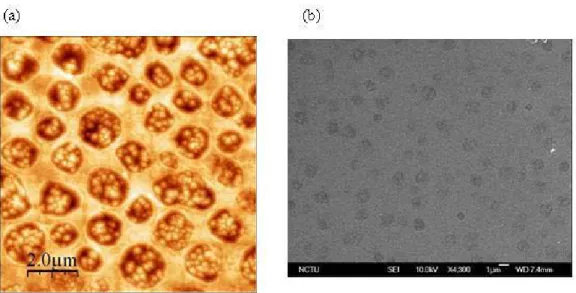
TMAH is non-pollutant and non-toxic, and is widely used to manufacture a pyramidal structure. In many research, the Si wafer with texturing surface etched by TMAH is often used to produce solar cell and other optoelectronic devices [51-52]. In our study, we adjust the etching temperature, the concentration of TMAH solution, and add appropriate surfactant to grow the optimized pyramidal structure, follow by characterizations of surface morphology and reflectivity.
Anisotropic etching of silicon is a major way to fabricate the three-dimensional pyramidal structures with low reflectivity and high surface area. All etching experiments are carried out using the single-crystalline [100] p-type silicon wafer as source materials. In this experiment, the texturing process is approached by using TMAH solution due to the low contamination and good etching characteristics that have been mentioned before. Because the etching rate depends on the composition, temperature and the properties of silicon surface, the optimized setup of etching conditions with respect to the concentration of solution and the environment effect needs to be considered. The results of silicon wafers etched with TMAH solutions with different concentrations and varying temperature are investigated. Before the etching process, the wafers are immersed in Buffered Oxide Etch (BOE) solution to remove oxide contaminations. Here we induce the characterization of the surface morphology based on the scanning electron microscope (SEM) and atomic force microscope (AFM). To determine the influence of etching temperature, experiments are carried out at temperatures ranging from 60 °C to 80 °C in the water batch and agitate the etching solution at the seed of 100 rpm. The SEM and AFM morphology of the wafers etched in 2.38 % TMAH solution at 60 °C, 70 °C and 80 °C are shown in figure 3-2, 3-3 and 3-4.
19
Figure 3-2 The morphology of silicon anisotropic etched in 2.38 % TMAH solution at 60 °C for 60 min. (a) shows the AFM morphology in 10 μm × 10 μ m area, and (b) shows the SEM morphology.
Figure 3-3 The morphology of silicon anisotropic etched in 2.38 % TMAH solution at 70 °C for 60 min. (a) shows the AFM morphology in 10 μm × 10 μ m area, and (b) shows the SEM morphology.
20
Figure 3-4 The morphology of silicon anisotropic etched in 2.38 % TMAH solution at 80°C 60 min. (a) shows the AFM morphology in 10 μm × 10 μ m area, and (b) shows the SEM morphology.
According to figure 3-2 to 3-4, we can see that there are many bubbles sticking on the surface, and these bubbles affect the growing of pyramidal structure. When the temperature increases, more hydrogen bubbles form on the silicon substrate. It has been known that the general texturing reaction could be described in figure 3-5 [53].
Figure 3-5 The reaction of general texturing silicon surface [53].
It is obvious that the reaction will generate hydrogen gas bubbles, which may stick on the silicon surface in the process of texturing. By adding isopropyl alcohol (IPA) as a surfactant, we find a tendency of bubble-adhering diminishment on the etched surface. IPA molecules clad the gas bubbles around and lift them off, thus the formation of big hydrogen bubbles can be avoided. Moreover, the higher temperature kept during texturing process, the faster bubbles been lift off [51].
21
Here we prepare solutions containing TMAH and IPA for avoiding the formation of big hydrogen bubbles on the surface of silicon wafer. Figure 3-6 to 3-8 show the AFM and SEM morphology of silicon anisotropic etched in 1.67 % TMAH and 30 % IPA at 60 °C, 70 °C, and 80 °C, respectively.
Figure 3-6 The morphology of silicon anisotropic etched in 1.67 % TMAH and 30 % IPA at 60 °C for 60 min. (a) shows the AFM morphology in 10 μm × 10 μm area, and (b) shows the SEM morphology.
Figure 3-7 The morphology of silicon anisotropic etched in 1.67 % TMAH and 30 % IPA solution at 70 °C for 60 min. (a) shows the AFM morphology in 10 μm × 10 μm area, and (b) shows the SEM morphology.
22
Figure 3-8 The morphology of silicon anisotropic etched in 1.67 % TMAH and 30 % IPA solution at 80 °C for 60 min. (a) shows the AFM morphology in 10 μm × 10 μm area, and (b) shows the SEM morphology.
Figure 3-9 The relationship of the average height of the etched silicon as a function of temperature.
23
From figure 3-6 to 3-8, we can conclude the influence of etching temperature. The etching rate of (100) and (110) crystallographic planes increases more rapidly than that of the (111) crystallographic plane at increasing temperature. When the temperature is increased, the difference in etching rate results in higher pyramids [36].
According to figure 3-6 to 3-8, the addition of IPA will diminish the adherence of hydrogen bubbles to the etched surface. However, there are still bubbles sticking on the surface leading to incomplete pyramidal structure formation during etching process. Here we prepare the TMAH and IPA solutions with distinct concentrations respectively, and the operation temperature is set at 80 °C, which brings to higher etching rate in figure 3-8. In order to prevent the hydrogen bubbles from sticking onto the silicon surface to form the pyramidal structure perfectly, we put the silicon wafer in vertical direction rather than in horizontal direction.
24
Figure 3-10 The AFM and SEM morphology of etched silicon etched by TMAH and IPA with different concentrations at 80 °C for 60 min. The concentrations of TMAH and IPA are 1.67 % and 30 % respectively in (a) (b), 1.19 % and 50 % respectively in (c) (d) and 0.714 % and 70 % in (e) and (f).
25
Figure 3-11 The resulting height of pyramidal structure etched in different concentration of TMAH and IPA at 80 °C.
Figure 3-10 and 3-11 indicate that the higher IPA content in the solution the more completely diminishment of hydrogen bubbles adherence on the etched surface, thus the growing of three-dimensional pyramidal structures can be improved. However, the solution with 0.714 % TMAH and 70 % IPA brings about lower average etching height and lower distribution of pyramidal structures. That reason may result from the lacking in the etching ability to silicon due to fewer TMAH concentrations. Figure 3-10 and 3-11 shows the uniform of growing pyramidal structures morphology and higher average etching height under the solution with 1.19 % TMAH and 50 % IPA.
In this experiment, we have optimized the texturing solution contains 1.19 % of TMAH and 50 % of IPA under the temperature of 80 °C. The optimization process of growing the three-dimensional pyramidal structures is for the sake of decreasing
26
reflectivity and the increasing surface area of silicon substrate [51]. The analysis method of N&K analyzer is discussed in chapter 4.
3.3 MSM Photodetector process
Figure 3-12 The manufacturing process of MSM photodetectors and PN diodes.
To fabricate MSM photodetectors, we utilize the 30μm-thick p-type Silicon thin chips that manufactured before, and put a digitated shadow mask covering over the silicon thin chips. Then we use thermal coater to coat 10 nm Cr and 100 nm Au digitated electrodes on the top of silicon thin chips, and then the chips are followed by coating 10 nm Cr and 100 nm Au electrodes at the bottom of the chips.
27
3.4 PN diode Process
To fabricate PN diodes, first we use the 30μm-thick p-type Silicon thin chips that manufactured before, make phosphorous (n-type) ion implantation on the top side, and put a digitated shadow mask covering over the silicon thin chips. Then we use thermal coater to grow 10 nm Cr and 100 nm thick Au digitated electrodes on the top of silicon thin chips, and coat 10 nm Cr and 100 nm thick Au electrodes at the bottom of the chips.
3.5 NPN transistor Process
Figure 3-13 The manufacturing process of NPN transistors.
28
chips that manufactured before, make phosphorous (n-type) ion implantation on the both sides, and put a digitated shadow mask covering over the silicon thin chips. Then we use thermal coater to grow 10 nm Cr and 100 nm thick Au digitated electrodes on the top of silicon thin chips, and coat 10 nm Cr and 100 nm thick Au electrodes at the bottom of them.
3.6 Solar Cell Process
Figure 3-14 The manufactuing process of solar cells.
To fabricate solar cells, first we utilize the 30μm-thick p-type silicon thin chips that manufactured before, make phosphorous (n-type) ion implantation on the top
29
side, and put a crisscross shadow mask covering over the silicon thin chip. Then we use thermal coater to grow 10 nm Cr and 100 nm thick Au crisscross electrodes on the top of silicon thin chips, and coat 10 nm Cr and 100 nm thick Au electrodes at the bottom of them.
30
Chapter 4 Results and Discussion
4.1 The Silicon Thin Chip by Etching
After etching for 49 hours, the 675μm-thick silicon wafers has been leveled down to chips with the thickness of 30 μm. The 30μm-thick silicon chips are thin enough to be bendable, and the flexible electronics in this experiment are base on these silicon thin chips. The XRD data reveals the silicon thin chips remaining single-crystalline in microstructure. The mobility of the silicon thin chips is an important parameter that determines whether the samples can be excellent devices or not, thus we measure the Hall mobility in this experiment. The Hall mobility of the silicon thin chips is 773 cm2 /V-S, which is better than that of amorphous silicon and polycrystalline silicon.
(a) (b)
Figure 4-1 The ultrathin silicon chips after etching. (a) optical image of 30μ m-thick silicon chip (b) optical image of 30μm-thick silicon chip with electrode film.
31
Figure 4-2 The croess-section SEM image of the 30μm-thick ultrathin silicon chip.
The 30μm-thick silicon thin chips have good flexibility and little brittle nature, so we choose the silicon chips with a thickness of 30μm to fabricate our electronic devices. The etching process levels down the silicon wafer thickness from 675μm to 30μm, and the thickness of the chips deviates within 5μm.
32
(a)
33
(c)
Figure 4-3 X-Ray diffraction measurement of ultrathin silicon chips. (a) The database of silicon. (b) X-Ray diffraction diagram of bulk 675μm-thick silicon wafer. (c) X-Ray diffraction diagram of ultrathin 30μm-thick silicon chip.
Comparing (b) with (C) , it is obvious that the ultrathin 30μm silicon chips are still single crystalline.
34
Figure 4-4 The Hall mobility of ultrathin silicon chip is 773 cm2/V-S.
The Hall mobility shown in Figure 4-4 is 773 cm2/V-S, which is close to
commercial single crystalline silicon wafer, and the XRD data shows that the structure of thin silicon chip are still single crystalline.
35
4.2 Optimal Conditions of Anisotropic Texturization
4.2-1 Surface Morphology of the Pyramidal Structure and Its
Reflectivity Analysis
As mentioned in chapter 3-2, we have determined the optimized etching solution of silicon wafer is 1.19 % of TMAH including 50 % of IPA under the temperature of 80 °C. The anisotropic texturization usually leads to pyramidal structures; moreover, the higher pyramids go along with more surface areas. Therefore, we discuss the optimal texturing time for growing the optical pyramidal structures, and analyze the reflectivity by N&K analyzer and the surface energy by contact angle. Figure 4-5 indicates the morphology of silicon wafers etched in 1.19 % of TMAH and 50 % of IPA at 80 °C with different texturing times, and the silicon wafers are all carried out in vertically direction.
36
Figure 4-5 The AFM and SEM texturing morphology of silicon wafers etched in 1.19 % of TMAH and 50 % of IPA at 80 °C with varying time. (a) and (b) are the morphology of silicon wafers textured for 30 min; the texturing time is 60 min for (c) and (d); 90 min for (e) and (f); and 120 min for (g) and (h).
37
According to figure 4-5, longer etching time gives rise to higher density of pyramidal structures on the silicon wafer and faster etching rate of the (100) and (110) crystallographic planes compared with the etching rate of the (111) crystallographic plane. The morphology of pyramidal structures can be observed from the SEM. The different etching time results in the different average height of the pyramidal structure shown in figure 4-6. With longer etching time, the process leads to a faster etching rate and gives rise to the growing of higher pyramidal structures.
Figure 4-6 Average height of pyramidal structures with different etching time. The highest density and optimal pyramids result from the 120 min processing time, and the average height is 3.01 μm.
38
The etching mechanism of TMAH follows alkaline silicon etching and can be classified into three separate steps [54-56]:
The mechanism reactions takes place on the silicon surface. In the first step, equation 2, TMAH molecular dissociate into hydroxyl ions. In the second step (Eq. 3), the silicon atoms at surface react with these hydroxyl ions and form oxidized silicates Si(OH)
2 2+
and four electrons are injected from each silicon atom into the conduction band. Simultaneously, water is reduced to provide more hydroxyl ions which are bonded to the silicate formed in second step. The reaction of equation 4 and 5 produce soluble silicic acid, with hydrogen gas as a byproduct. As shown in previous equations, it means the water will present and the silicon will be etched. When the concentration of water increases, more hydrogen forms and therefore more bubbles present. However, the bubbles will stick on the silicon surface and affect the etching rate as discussed in chapter 3-2. The bubbles on the surface will block the reactants and products from diffusing thus a depletion region forms. The hydrogen generated on the silicon surface forms bubbles which can reduce the natural upward flow between the solution and silicon surface and causes some difficulties in etching rate. We add the IPA as the surfactant to diminish the adherence of hydrogen bubbles on
39
the etched surface. Therefore, roughness increases during etching time due to the progressive etching rate in (100) and (110) directions, and finally pyramids with surrounding (111) planes leave behind.
In addition, the texturization efficiency depends on the concentration of etching solution, temperature and etching time. It provides an alternative method to create uniform and reproducible pyramidal texture on silicon wafer with the help of isopropyl alcohol (IPA) surfactant and agitation. Since the amount of water and IPA present in the solution increases in same time and less hydrogen produced when TMAH concentration decreases, therefore the roughness increases. Initially, a small number of pyramids forms at the surface, as etching process continues, new pyramids form and begin to superimpose over previous hillocks. The number and the size of the pyramids are observed by SEM and the average height is observed by AFM.
With the growing of pyramidal structures, the difference of etching rate results in higher pyramids and leads to a lower reflectivity shown in figure 4-7. By textural effects, the reflectance of pyramidal structures is lowered within all wavelengths. The higher pyramids leads to a lower reflectivity hence the light absorption is increased, and this absorption can be further improved by an optimized texturization [51]. In this experiment, the best condition of anisotropic texturization is etching under the condition of 1.19 % TMAH and 50 % of IPA solution at 80 0C for 120 min. For the sake of electrode manufacturing, we coat 5 nm-thick Cr and 10 nm-thick Au on the optimal texturing silicon substrate. The resulting reflectivity is relatively lower than untreated sample shown in figure 4-8. The reflection of the front surface needs to be minimized and the incident light must shine into the valley of the pyramids to increase the ability of light collection and promote high efficiency of silicon solar cells. This improvement was recently achieved by an anisotropic textured surface covered by a gold film [57], and shows a large decrease of the reflectance over the entire spectrum.
40
This difference is explained by light trapping [58-60] improvement for following detection.
Figure 4-7 Comparison of the reflectivity of silicon surface with pyramidal structures during with different texturing time.
41
process by N&K analyzer. The reflectivity of TMAH-textured silicon substrate with a thin gold film is down to 2.00 % at 400 nm light wavelength.
4.2-2 Surface Energy of the Pyramidal Structure
The definitions of surface energy involve consideration of the behavior of liquids in contact with solids materials and the formation of droplets. One convenient way of quantifying this behavior is to measure the contact angle formed by the liquid-solid interfaces shown in figure 4-9. The total surface energy is based on the Young–Dupre equation, which is described by the interfacial tension between the liquid (L) and the polymer surface (S) [61]:
The equation 6 is together with the Lifshitz–van der Waals (LW) and Lewis acid–base (AB) theories. The equation 7 is the surface tension (γ
i) of a phase i, and γi
+
and γi– are the electron acceptor and electron donor parameters, respectively. The contact angle θ is determined using three different liquids with water, ethylene glycol and diiodomethane. The surface properties of optimal textured process are studied by the drop contact-angle technique shown in table 4-1. The total surface energy can be calculated from the contact angles of water, ethylene glycol, and diiodomethane. According to the Young–Dupre equation, the contribution of van der Waals (γ
S
LW
) surface tension is broader than acid–base (γ
S
+
, γS– ), and therefore the textured surfaces provide the apolar interface in table 4-2. The longer etching time leads to higher surface energy and relatively unstable surface due to larger surface area and surface tension [62]. However, when coating with a gold thin film, the total surface energy
42
becomes lower which represents more stable surface. When we drop the liquid, the water drop become spreading out over the surface and the contact angle tends to be 5.97 degree, and it means the textured surface is super-hydrophilic.
Figure 4-9 The drop of DI water on the gold thin film coating on the textured surface. The contact angle of water droplet and film is 30.2 degree which means the hydrophilic feature of optimal texturing substrate etched on the conditions of 1.19 % TMAH and 50 % of IPA solution at 80 0C for 120 min.
43
Table 4-1 The measurement of contact angle with different etching time by 1.19 % TMAH and 50 % of IPA solution at 80 0C.
Table 4-2 The measurement of surface tension and total surface energy with different etching time.
44
4.3 Electrical Properties of flexible devices
Because the devices are made from single crystal silicon, they provide great electrical properties. The electrical properties are shown in the figures below.
4.3-1 Electrical Properties of MSM Photodetector
I-V measurements of MSM photodetectors were carried out using a halogen
lamp incident from the object lens of optical microscopy in a dark environvent, and the wavelength is ranged in visible light region. Since our goal is to detect the light, the ratio of the light current (photo current, IL) to dark current (ID) is the main
characteristic we concern with. We focus on this issue in this section. The definitions of dark current and photo current are the current responses without and without light illuminating respectively.
We use a calibration photodiode to measure the power of the halogen lamp. The calibration photodiode has a filter that only wavelengths between 300nm~ 800nm can pass through the filter and absorbed by the photodiode. While the photo current generated by the photodiode equals 1 mA, the power of the incident light is equivalent to 100 mW/cm2. The photodiode operates at reverse-biased region.Figure 4-10 shows the halogen lamp power intensity. In the following experiment, the power of the lamp which can be controlled by a roll knob equals to 1.46 mW/cm2 if not mentioned.
45
Figure 4-10 Power intensity of the halogen lamp measured by the calibration photodiode.
Figure 4-11 shows I-V characteristics of MSM photodetectors. From Figure 4-12, the ratio of photo current density to dark current density that operates at 5V is 562. The photo current and the dark current at 5 V are 2.7397 μA and 0.00486 μA respectively. In the small voltage region (~0.1V), the electric field which results from applied voltage may not be strong enough to separate the photo-induced electrons. As the applied voltage gets larger and larger, the corresponding electric field gets stronger at the same time, hence more electrons can be collected and finally results in larger photo current.
46
Figure 4-11 The I-V characteristic of the MSM photodetector with interdigitated lines.
Figure 4-12 The dark and light I-V characteristic of the MSM photodetector with interdigitated lines.
47
Good mechanical flexibility is extremely important for flexible electronics applications. We evaluate flexibility by performing repeatedly frontward and backward bending tests. Afterward we measure the device bent for 1~20000 times to check the stability. As shown in Figure 4-13, the dark current density and photo current density at 5V are very stable with different bending times. We also measure the durability with different bending radius (0.5~10 cm) to test the critical deformation condition. As shown in Figure 4-14, the devices deformed from 10 cm to 0.5 cm in radius perform little change in dark current density and photo current density at 5V. In Figure 4-15 we can find out the device is considerably stable, and the difference of current density between the devices unbent and bent for 100 times is around 2.1%.
48
Figure 4-14 The dark and light I-V characteristic of the MSM photodetectors bent with various curvature radius.
Figure 4-15 The difference of I-V characteristic between MSM photodetectors unbent and bent for 100 times.
49
4.3-2 Electrical Properties of PN Diode
Figure 4-16 shows the I-V measurement of a PN diode, and the ratio of ON/OFF current is 25120. From Figure 4-17, the ratio of photo current density to dark current density operation at -1V is 6.31. The photo current and the dark current at -1V are 0.00126 μA and 0.0002 μA respectively. In the small voltage region (~0.001V), the electric field which results from applied voltage may not be strong enough to separate the photo-induced electrons. As the applied voltage gets larger and larger, the corresponding electric field gets stronger at the same time, hence more electrons can be collected and finally results in large photo current.
Figure 4-16 The I-V characteristic of the PN diode.
50
Figure 4-17 The dark and light I-V characteristic of the PN diode.
Good mechanical flexibility is extremely important for flexible electronics applications. We evaluate flexibility by performing repeatedly frontward and backward bending tests. Afterward we measure the device bent for 1~20000 times to check the stability. As shown in Figure 4-18, the dark current density and photo current density at -1V are very stable with different bending times. We also measure the durability with different bending radius (0.5~10 cm) to test the critical deformation condition. As shown in Figure 4-19, the devices deformed from 10 cm to 0.5 cm in radius perform little change in dark current density and photo current density at -1V. In Figure 4-20, we can find out the device is considerably stable, and the difference of current density between the devices unbent and bent for 100 times is around 0.7%. Figure 4-21 shows the current-time responses of MSM photodetectors at 1Vand PN diodes at -5V. The current of MSM photodetector and PN diode are
51
stable during scanning time, and the performance of MSM photodetector is relatively stable compared with the PN diode.
Figure 4-18 The durability of the PN diode.
Figure 4-19 The dark and light I-V characteristic of PN diodes bent with various curvature.
52
Figure 4-20 The difference of I-V characteristic between PN diodes unbent and bent for 100 times.
53
4.3-3 Electrical Properties of NPN Transistor
Figure 4-22 and 4-23 show the I-V measurements of NPN transistors in log and linear scale. The ratio of photo current density to dark current density operation at 1V is 8.47. The photo current and the dark current at -1V are 4.858 μA and 0.5734 μA respectively. As the applied voltage gets larger and larger, the corresponding electric field gets stronger at the same time, hence more electrons can be collected and finally results in large photo current.
54
Figure 4-23 The I-V characteristic of the NPN transistor in linear scale.
4.3-4 Electrical Properties of Solar Cell
Figure 4-24 shows the I-V measurement of a flexible solar cell carried out under the illumination condition of AM 1.5 (1000W/m2 full-spectrum solar simulator at room temperature). Figure 4-25 shows a short-circuit current, Isc, of -2.0182 mA,
and open-circuit voltage, Voc, of 0.1088 V, a fill factor of 0.25, electrode area of
0.0363 cm2 and an overall solar-energy conversion efficiency (η) of 1.5%. The properties of the 30 μ m-thick solar cells are mainly ranged in 1~1.6% for solar-energy conversion efficiency (η) and 0.08~0.11 V for open-circuit voltage (Voc).
55
Figure 4-24 The I-V characteristic of the solar cell in linear scale (-10 V~5V).
56
Good mechanical flexibility is extremely important for flexible electronics applications. We evaluate flexibility by performing repeatedly frontward and backward bending tests. Afterward we measure the device which is bent for 1~20000 times to check the stability. As shown in Figure 4-26, dark current density and photo current density at 0.1V are very stable with different bending times. We also measure the devices with different bending radius (0.5~10 cm) to test the critical deformation condition. As shown in Figure 4-27, the devices deformed from 10 cm to 0.5 cm in radius perform little change in dark current density and photo current density at 0.1V. Figure 4-28 shows the current-time responses of solar cell and PN diode at 0.1V, and the current of solar cell is more stable compared with the PN diode.
57
Figure 4-27 The dark and light I-V characteristic of solar cell bent with various curvature.
58
Figure 4-29 Optical images of flexible solar cells with conductive copper tapes.
The types of modules reported in this study may create new possibilities for single-crystalline silicon photovoltanics, particularly in the applications that benefit from thin, lightweight construction, mechanical flexibility or the unusual optical properties of the flexible solar cells designs. In most cases, we chose materials that have potentials for long lifetime and high reliability. The procedures are compatible with substrates, encapsulation, adhesive and optical materials used in existing photovoltaic systems. Similarly, the designs of advanced single-crystalline silicon cell can also incorporate with enhancement techniques for improved performance. Although the main focuses presented here are based on module capabilities and designs rather than the cost or performance, these approaches of ultrathin cell geometry designs provide notable features in the efficient silicon usage. The process suggested here reduces the requirements for purity of the silicon, thus lowers the cost of silicon source materials. Low-cost doping and etching techniques are suitable for high-performance solar cells and module fabrication, together with other means to reduce cost or increase performance, are therefore important areas for further work.