國立交通大學
電子工程學系 電子研究所
碩 士 論 文
在多核心系統中考慮動態隨機存取記憶體讀/寫特性
以降低功率消耗之排程機制
A Read-Write Aware DRAM Scheduling for Power
Reduction in Multi-Core Systems
研 究 生: 賴之彥
指導教授: 周景揚 教授
在多核心系統中考慮動態隨機存取記憶體讀/寫特性
以降低功率消耗之排程機制
A Read-Write Aware DRAM Scheduling for Power
Reduction in Multi-Core Systems
研 究 生:賴之彥 Student: Chih-Yen Lai
指導教授:周景揚 Advisor: Jing-Yang Jou
國 立 交 通 大 學
電子工程學系 電子研究所
碩 士 論 文
A Thesis
Submitted to Department of Electronics Engineering and Institute of Electronics College of Electrical and Computer Engineering
National Chiao Tung University In Partial Fulfillment of the Requirements
for the Degree of Master of Science
in
Electronics Engineering
August 2013
Hsinchu, Taiwan, Republic of China
I
在多核心系統中考慮動態隨機存取記憶體讀/寫特性以降
低功率消耗之排程機制
學生:賴之彥 指導教授:周景揚 博士
國立交通大學
電子工程學系 電子研究所碩士班
摘 要
近幾年來,隨著市場及業界對於高效能、低功耗系統的需求,功耗管理的重要性已 日漸增加。在現今的多核心系統當中,動態隨機存取記憶體(DRAM)的功率消耗佔了整 個系統的一大部分,因此吸引了許多人研究 DRAM 的功耗管理。而除了功率消耗之外, DRAM 同時還是目前多核心系統中的效能瓶頸,所以在設計 DRAM 功耗管理的方法時, 必須格外地小心以避免大幅度地降低系統效能。目前關於 DRAM 功耗管理方法的研究 中,有大量的研究是透過 DRAM 的排程機制來排序指令以降低功率消耗。在此基礎上, 本篇論文提出考慮 DRAM 讀/寫特性的指令調節技術以及指令排程機制,在不影響系統 效能的前提下,進一步降低 DRAM 功率消耗。根據實驗結果,本篇論文提出的機制平 均能夠有效降低 75%的 DRAM 功率消耗。若與現有的方法比較,本篇論文所提出的機 制能夠在相同甚至是較少的系統效能損失之下,多降低 10%的 DRAM 功率消耗。II
A Read-Write Aware DRAM Scheduling for Power
Reduction in Multi-Core Systems
Student: Chih-Yen Lai Advisor: Dr. Jing-Yang Jou
Department of Electronics Engineering
Institute of Electronics
National Chiao Tung University
ABSTRACT
The demand of high performance and low power has increased the importance of power efficiency in multi-core systems. In modern multi-core architectures, DRAM has dominated the power consumption. Moreover, the performance of nowadays system is limited by the memory wall, which implies that a careless DRAM power management policy may harm the system performance dramatically. Among all the DRAM power management policies, reordering based DRAM scheduling has been widely studied to reduce the power. To further reduce the power while preserving the system performance, this thesis proposes the read-write aware throttling and the read-write reordering techniques. The proposed techniques effectively reduce 75% DRAM power on average. When compared to the existing work, the proposed techniques reduce 10% more power with comparable or less performance degradation on average.
III
Acknowledgements
First and foremost, I would like to express my deepest appreciation to my advisor, Dr. Jing-Yang Jou for his patient guidance on my research. He also gave me many helpful suggestions about my career and motivated me to be a better person. I am sincerely grateful to my senior, Gung-Yu Pan for his kind guidance, direction and invaluable assistance. Discussions with him have been insightful, and I would never have been able to finish this thesis without his help. I would also like to thank my senior, Hsien-Kai Kuo for his useful suggestions. I appreciate all the members of EDA Lab, Bu-Ching Lin, Yung-Chun Lei, An-Che Cheng, and Chin-Fu Lu, for all your supports and for all the fun we have had together.
I would like to offer my special thanks to all my friends, including but not limited to: Chuan-Chia Huang, Kuan-Ting Chen, Kuan-Chang Wang, Yi-Jing Liu, Wen-Xuan Yu, for making my daily life joyful. Special thanks also go to all my teammates in NCTU EE volleyball team for filling up my life in the past six years, especially Ping-Yuan, Tsai, who has been a great help in tutoring me in almost every course I took. Thank all my lovely players in NCTU EE girl volleyball team, it was an honor coaching you. In particularly, I would like to thank Chia-Ying Li for her assistance on many chores. I would also like to thank Samantha Koch, who gave me a lot of thoughts about my life.
Finally, I owe my deepest gratitude to my parents and my sister. Their endless support and love have always been encouraging. They have provided me a carefree environment so I can concentrate on my study. I am so lucky to be in such a wonderful family. At last but not least, thank my girlfriend, Chen-Huan Yen for being a huge part in my life. She stood by me through the good times and bad. I would not be who I am without her love.
IV
Contents
摘 要 ... I ABSTRACT ... II Acknowledgements ... III Contents... IV List of Figures ... V List of Tables ... VI Chapter 1 Introduction ... 1 1.1 DRAM Architecture ... 11.2 Reducing the DRAM Power ... 5
1.3 Related Works and Motivation ... 7
1.4 Our Contributions ... 11
Chapter 2 Problem Description ... 12
2.1 System Model ... 12
2.2 Problem Statement ... 18
Chapter 3 The Proposed Techniques ... 19
3.1 Overview ... 19
3.2 Read-Write Aware Throttling ... 25
3.3 Rank Level Read-Write Reordering ... 29
3.4 An Example of The Proposed Policy ... 33
Chapter 4 Experimental Results ... 36
4.1 Simulation Environment ... 36
4.2 Analysis on Different Techniques ... 40
4.3 Power and Performance Trade-Off ... 47
Chapter 5 Conclusions and Future Works ... 56
V
List of Figures
Fig. 1 The architecture of a DIMM, which includes ranks and banks, inside the DRAM. ... 2 Fig. 2 Example of how a sequence of read commands to the same row is carried out inside
a DRAM bank. ... 3 Fig. 3 Power mode transition delays. ... 6 Fig. 4 System hierarchy diagram and the architecture of queues inside the memory
controller. ... 12 Fig. 5 An example of how the blocked memory commands transfer from the RQ to the CQs
when the throttle delay is reached in a throttling mechanism. ... 15 Fig. 6 Flow chart of a greedy memory controller, which employs the greedy power-down
policy. ... 19 Fig. 7 Flow chart of the memory controller proposed in the previous work [21]. ... 21 Fig. 8 Flow chart of the memory controller employing the proposed techniques. ... 23 Fig. 9 An example of how commands blocked in the RQ are clustered into command sets.... 26
Fig. 10 An example of how commands in a given command set S1 are combined into
command groups and then reordered... 30 Fig. 11 An example of how the read-write aware throttling clusters commands in the RQ
and determines which ranks should be turned on when the throttle delay is reached. ... 33
Fig. 12 An example of how the commands in a given command set 𝑆1 are reordered by
the rank level read-write reordering and sent to the CQ... 34 Fig. 13 Power and performance of different policies on different benchmark combinations. . 41 Fig. 14 The background power, ACT/PRE power, and the read/write power consumptions
of different techniques. ... 45 Fig. 15 Average power and performance trade-off characteristics on SPEC CPU2006 [31]. .. 49 Fig. 16 Power and performance trade-off characteristics for fp1. ... 50 Fig. 17 Power and performance trade-off characteristics for fp3. ... 50 Fig. 18 Average power and performance trade-off characteristics on SPLASH-2 [32]. ... 51
VI
List of Tables
Table I Table of abbreviations ... 16
Table II Table of notations ... 17
Table III Configuration parameters of ARM Cortex A9 [30] ... 37
Table IV Memory system parameters ... 38
Table V Benchmark combinations of floating-point benchmarks in SPEC CPU2006 [31] ... 38
Table VI SPLASH-2 [32] benchmarks used in the evaluation ... 39
Table VII Read requests percentage of each benchmark combination ... 43
Table VIII Effect of different throttle delays ... 48
Table IX Main memory requests per million cycles of different benchmarks ... 52
Table X Detail evaluation results on different throttle delays for SPEC CPU2006 [31] ... 53
1
Chapter 1
Introduction
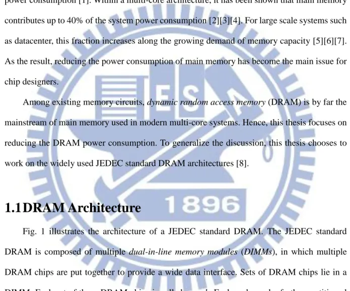
In the latest multi-core systems, the increasing performance comes at the cost of the higher power consumption [1]. Within a multi-core architecture, it has been shown that main memory contributes up to 40% of the system power consumption [2][3][4]. For large scale systems such as datacenter, this fraction increases along the growing demand of memory capacity [5][6][7]. As the result, reducing the power consumption of main memory has become the main issue for chip designers.
Among existing memory circuits, dynamic random access memory (DRAM) is by far the mainstream of main memory used in modern multi-core systems. Hence, this thesis focuses on reducing the DRAM power consumption. To generalize the discussion, this thesis chooses to work on the widely used JEDEC standard DRAM architectures [8].
1.1 DRAM Architecture
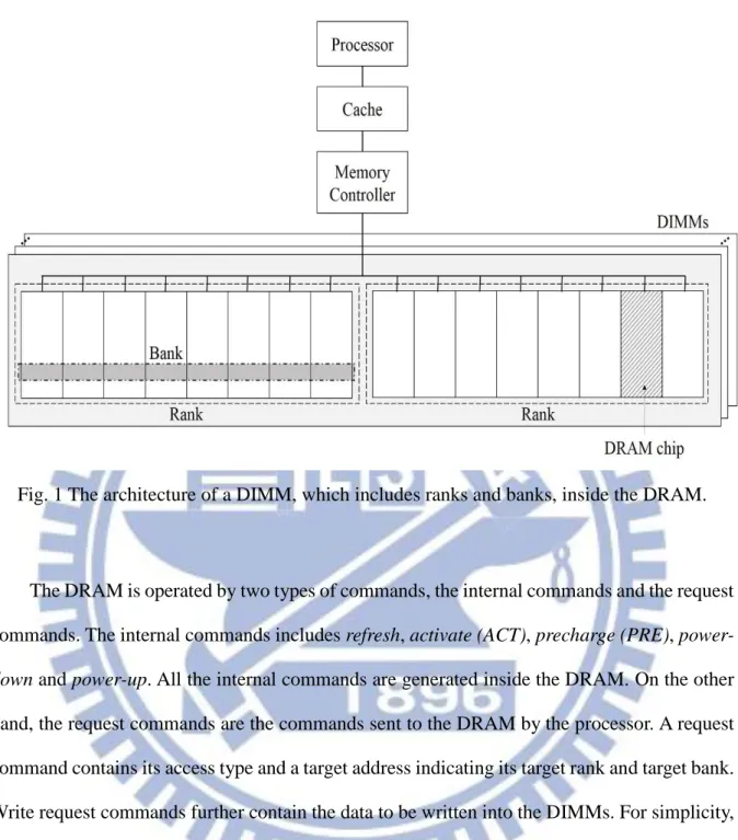
Fig. 1 illustrates the architecture of a JEDEC standard DRAM. The JEDEC standard DRAM is composed of multiple dual-in-line memory modules (DIMMs), in which multiple DRAM chips are put together to provide a wide data interface. Sets of DRAM chips lie in a DIMM. Each set of these DRAM chips is called a rank. Each rank can be further partitioned into banks, which spread across all DRAM chips within a rank. Each bank is organized as a
two-dimensional array and its size is defined as 𝑟𝑜𝑤𝑠 × 𝑐𝑜𝑙𝑢𝑚𝑛𝑠. Only a single row of data
can be accessed at any given time. Each bank has its own row buffer to store the row of data that is ready to be accessed [9]. Since the DRAM is a volatile memory, the data stored in the array need to be periodically refreshed to prevent data loss.
2
Fig. 1 The architecture of a DIMM, which includes ranks and banks, inside the DRAM.
The DRAM is operated by two types of commands, the internal commands and the request commands. The internal commands includes refresh, activate (ACT), precharge (PRE), power-down and power-up. All the internal commands are generated inside the DRAM. On the other hand, the request commands are the commands sent to the DRAM by the processor. A request command contains its access type and a target address indicating its target rank and target bank. Write request commands further contain the data to be written into the DIMMs. For simplicity, in the remainder of this thesis, the term memory command refers to the memory request command if not specified.
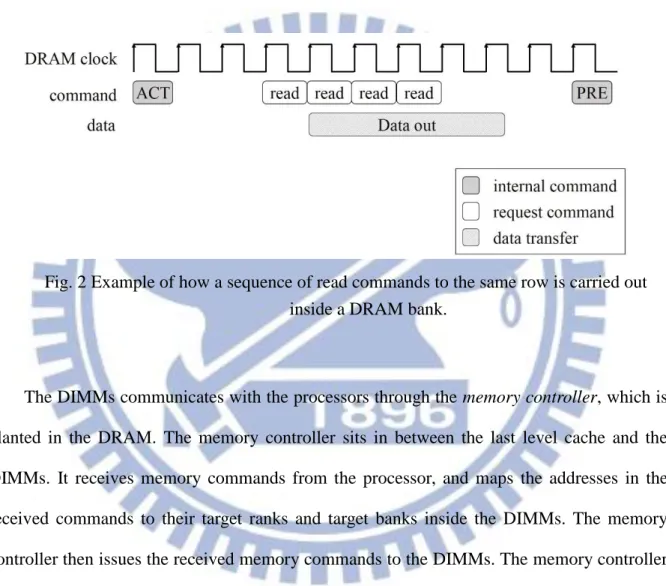
For a memory command to access a location in the DIMMs, several internal commands are triggered to carry out the read or write request. First, all the DRAM chips in the target rank of the memory command need to be activated. The DRAM generates an ACT command and sends it to the target bank of the memory command. The ACT command activates all the DRAM chips in the bank and reads out an entire row of data. This row of data is stored in the row buffer.
3
The data can either be read from or written to a column, which is indicated by the memory command, inside the fetched row. After the request completes, the DRAM send a PRE command to the open bank. The PRE command restores the data from the row buffer to the memory array inside the bank [10]. Fig. 2 shows an example of how a sequence of continuous read commands to the same row are carried out inside a DRAM bank.
Fig. 2 Example of how a sequence of read commands to the same row is carried out inside a DRAM bank.
The DIMMs communicates with the processors through the memory controller, which is planted in the DRAM. The memory controller sits in between the last level cache and the DIMMs. It receives memory commands from the processor, and maps the addresses in the received commands to their target ranks and target banks inside the DIMMs. The memory controller then issues the received memory commands to the DIMMs. The memory controller is able to reorder the memory commands while preventing data hazards. The memory controller is also in charge of generating the internal commands such as ACT, PRE, and refresh. The memory controller can switch the power mode of a rank by generating down or power-up commands.
The master operation of a DRAM chip is controlled by the corresponding clock enable (CKE) signal. When CKE is low, all inputs, including DRAM clocks, are disabled [11]. If the
4
CKE for a DRAM chip is low, that DRAM chip is considered to be in the off mode. None of the request commands or the internal commands can be processed by a DRAM chip when it is in the off mode. The only exception is the refresh command. Even when a DRAM chip is in the off mode, it has to be periodically refreshed in order to retain data integrity in itself. The DRAM clocks start propagating through a DRAM chip when the CKE is risen to high. The DRAM chip begins taking inputs and processes the received memory commands. The DRAM chip is considered to be in the on mode when the CKE is high.
5
1.2 Reducing the DRAM Power
The power consumption of the DRAM consists of several different components. First of all, the DRAM continuously consumes a background power. The value of the background differs from the mode of the DRAM chip. When the DRAM chip is in the off mode, the
background power is defined to be 𝑃𝑃𝐷𝑁. The background power is defined to be 𝑃𝐴𝐶𝑇_𝑆𝑇𝐵𝑌
when the DRAM chip is in the on mode. It is natural that 𝑃𝐴𝐶𝑇_𝑆𝑇𝐵𝑌 is larger than 𝑃𝑃𝐷𝑁; for modern DRAM circuits, 𝑃𝑃𝐷𝑁 is just 6.67%~15.38% of 𝑃𝐴𝐶𝑇_𝑆𝑇𝐵𝑌 [10][11]. The periodic refresh operation consumes the refresh power (𝑃𝑅𝐸𝐹). Finally, active power (𝑃𝐴𝐶𝑇), precharge power (𝑃𝑃𝑅𝐸), and the read or write power (𝑃𝑅𝐷 or 𝑃𝑊𝑅) are average power needed for all memory accesses. To sum up, the power consumptions of the DRAM can be written as:
𝑃𝑜𝑓𝑓 = 𝑃𝑃𝐷𝑁+ 𝑃𝑅𝐸𝐹 (1) 𝑃𝑜𝑛 = 𝑃𝐴𝐶𝑇_𝑆𝑇𝐵𝑌+ 𝑃𝑅𝐸𝐹+ 𝑃𝐴𝐶𝑇+ 𝑃𝑅𝐷+ 𝑃𝑊𝑅+ 𝑃𝑃𝑅𝐸, (2)
where 𝑃𝑜𝑓𝑓 and 𝑃𝑜𝑛 represent the power consumption of DRAM chips in the off mode and
on mode respectively. The power consumption of DRAM chips in the off mode is the lowest power in which DRAM chips may keep the data integrity, and the off mode is therefore known as the low power mode.
Since the DRAM chips consume less power when they are in the low power mode, the DRAM chips that are idle should be turned off in order to reduce the DRAM power. Due to the fact that all the DRAM chips inside a rank need to be activated for a memory access, it is impossible to turn off a single DRAM chip alone. Therefore, a rank is the smallest set of DRAM chips that can be turned off. The JEDEC standard DRAM supports rank level power mode control and allows users to turn on or turn off each rank separately [8][12].
6
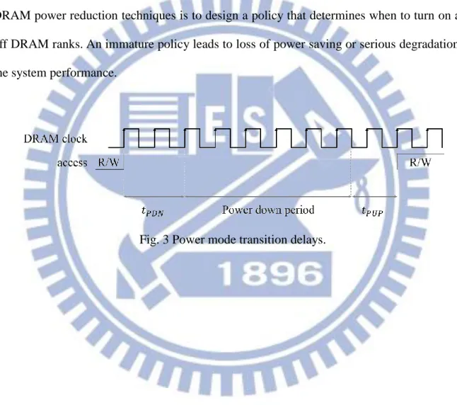
Although turning off idle ranks reduces the DRAM power, switching power mode of a rank takes a transition delay of time. Fig. 3 illustrates the power mode transition delays between two memory accesses, which can either be read or write (R/W). In Fig. 3, the memory accesses are depicted as rectangles, whereas 𝑡𝑃𝐷𝑁 and 𝑡𝑃𝑈𝑃 represent power-down transition delay and power-up transition delay respectively. The delays of switching power mode of ranks bring extra latencies to the system performance. Therefore, one of the main goals for designing DRAM power reduction techniques is to design a policy that determines when to turn on and off DRAM ranks. An immature policy leads to loss of power saving or serious degradation to the system performance.
7
1.3
Related Works and Motivation
Many different types of approaches toward DRAM power reduction have been studied in recent years. These approaches include designing a hybrid main memory, re-designing the physical structure of the DRAM, adding hardware component to the DRAM and designing power management policy for the memory controller in the modern DRAM.
Designing a hybrid main memory aims to reduce the DRAM power consumption by cutting down the refresh energy consumed by the DRAM. Phase change random access memory (PCRAM) is used in the hybrid memory as a large background main memory since it consumes low standby power. The DRAM serves as a cache above PCRAM [13][14]. The data in DRAM decay over time and are written back to the PCRAM if they are dirty. The DRAM refresh energy is thus reduced. Besides integrating PCRAM with DRAM, some proposed to use the cached DRAM, which adds a cache directly into the memory device [15]. Adding cache to the DRAM reduces the access to DRAM chips and thus increases the idle period. Therefore, the DRAM chips can be put to the low power mode to save more power.
Re-designing the physical structure of DRAM targets to improve the granularity of DRAM power mode control, which increases the potential of turning off idle DRAM chips. Some proposed to separate ranks into mini-ranks by adding mini-rank buffers inside each rank [16]; others proposed to change the arrangement of arrays in each bank [2]. These approaches allow the memory controller to switch the power mode of a set of DRAM chips, which the number of chip is smaller than that contained in a rank. It is more likely for DRAM chips in a smaller chip set to be all idle. Therefore, the memory controller has more chance to turn off idle chips and thus reduces the DRAM power consumption.
Both designing hybrid main memories and re-designing the physical structure of the DRAM have the potential to achieve good performance. Nevertheless, they both require big modifications to the modern DRAM architecture. Since this thesis aims to design power
8
reduction techniques for DRAMs that are commonly used in nowadays multi-core systems, these approaches are not suitable.
A different type of approaches reduce the DRAM power by adding some extra hardware to the existing DRAM circuit and extend its capability. For example, retention-aware intelligent DRAM refresh mechanism identifies and skips unnecessary refreshes for the DRAM [17]. By only refreshing necessary rows in DRAM banks, the refresh power is cut down. Another example is automatic data migration, which migrates data from ranks to ranks and tries to make the memory access concentrate on certain ranks [18]. This creates more empty ranks, which do not need to be periodically refreshed and can be completely shut off for a period of time. However, these approaches require a large hardware overhead to implement.
In order to reduce the DRAM power consumption without a big modification to the modern DRAM circuits, many approaches design power management policies for the memory controllers. The policies can be categorized into power-down policies, which determine when to turn an idle rank off; scheduling policies, which schedule the commands in the memory controller; throttling-based policies, which block command in the buffer to prolong the idle period of a rank.
An intuitive power-down policy is the time-out power-down policy [19]. The time-out power-down policy turns off a rank once it is idle for a pre-defined, fixed period of cycles, regardless of the upcoming command pattern. This results in inflexible power mode transitions, which may turn off the DRAM ranks even during a short idle period or waste active standby power waiting for the timer to expire. Therefore, the time-out power-down policy does not guarantee an acceptable power reduction and may harm the system performance dramatically [20]. Besides the time-out power-down policy, queue-aware power-down policy is proposed [21]. In the queue-aware power-down policy, if a rank is idle, commands in the memory controller are checked to see if any of the pending commands is destined for the idle rank. If there is no pending commands heading to the idle rank, it is turned off. The aggressive
9
bandwidth-neutral strategy proposed in [22] is a policy derived from the queue-aware power-down policy with an additional snooping mechanism that turns the idle ranks back on upon receiving a memory command in the memory controller. The queue-aware power-down policy and the aggressive bandwidth-neutral strategy do not affect the system performance as much as the time-out power-down policy does, but their effect on reduction DRAM power is limited because they do not maximize the ability of the memory controller.
The scheduling policies are also known as schedulers. Some schedulers stress on scheduling both request commands and internal commands [9][23][24]. These schedulers require extra hardware to allow the memory controller arranges all the commands more sophisticatedly to reduce the DRAM power. Other schedulers focus on scheduling only the request commands. Since the memory controller reorders request commands while preventing data hazards even when no power management policy is employed, scheduling request commands does not add extra hardware to the memory controller. Among this type of schedulers, the power-aware memory scheduler is proposed in [21]. The power-aware memory scheduler clusters memory commands destined for the same rank together. While the memory concentrates on accessing one rank, other ranks can be switched to the low power mode to save power. Since only a single rank is activated at a time, other ranks stay in the low power mode for longer periods.
The throttling-based policies restricts memory access commands to be issued to the DIMMs to reduce the DRAM power [21][25]. The memory throttling mechanism proposed in [21] increases the power saving by blocking memory commands in the memory controller and force the DRAM chips to stay idle. No command is issued by the memory controller before it has blocked commands for a fixed period of cycles. This fixed period of cycles is called the throttle delay (𝑡𝑇𝐷).
With the queue-aware power-down policy, power-aware scheduler and the memory throttling mechanism, the previous work [21] achieves a power saving closed to time-out
10
power-down policy with a moderate system performance degradation. However, the previous work [21] does not take into consideration that read requests are more critical for the system performance than write requests [26]. In modern multi-core systems, a higher write latency can be tolerated using buffers [27]. Therefore, slowing down the write accesses does not impact the system performance much. Utilizing this fact, one can further reduce DRAM power consumption with a slight system performance overhead.
This thesis chooses to add new techniques based on the power-aware scheduler and the memory throttling mechanism proposed in the previous work [21]. However, all of the related works mentioned above are orthogonal to each other and can be integrated with the proposed techniques.
11
1.4
Our Contributions
To reduce DRAM power consumption, this thesis proposes the read-write aware DRAM scheduling, which utilizes the different criticalities between read accesses and write accesses. The DRAM scheduling mentioned in the remainder of this thesis refers to reordering the sequence of all the memory commands inside the memory controller. In this thesis, the internal DRAM commands such as ACT and PRE…etc. remain their default order and are not taken into consideration in the proposed techniques.
This thesis proposes two techniques, the read-write aware throttling mechanism and the rank level read-write reordering technique. The read-write aware throttling mechanism effectively cuts down DRAM power consumption. The rank level read-write reordering is employed to significantly reduces the system performance degradation caused by DRAM power management while maintaining the power saving. Our work reduces 75.34% of the DRAM power from the DRAM with no power management. When compared to the existing work, the proposed techniques reduce 10% more DRAM power with less performance degradation. Moreover, by evaluating and comparing with an oracle policy, the experimental results have shown that our work can reduce more power at the expense of a slight system performance degradation.
The remainder of this thesis is organized as follows. The next chapter describes the problem formulation. Chapter 3 places the proposed techniques. The experiment results are presented in Chapter 4. Finally, this thesis is concluded in Chapter 5.
12
Chapter 2
Problem Description
2.1 System Model
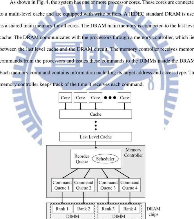
As shown in Fig. 4, the system has one or more processor cores. These cores are connected to a multi-level cache and are equipped with write buffers. A JEDEC standard DRAM is used as a shared main memory for all cores. The DRAM main memory is connected to the last level cache. The DRAM communicates with the processors through a memory controller, which lies between the last level cache and the DRAM circuit. The memory controller receives memory commands from the processors and issues these commands to the DIMMs inside the DRAM. Each memory command contains information including its target address and access type. The memory controller keeps track of the time it receives each command.
13
Within the memory controller, there are two queues: the reorder queue (RQ) and the command queues (CQs). Memory access commands from the last level cache are first stored in the RQ. These commands are mapped to certain DRAM ranks and banks according to their target addresses. A scheduler inside the RQ is able to reorder the commands in the RQ while keeping the data hazard-free. After mapping and reordering, the memory controller sends the memory commands from the RQ to the CQs one at a cycle. Each CQ corresponds to a certain rank. Therefore, for a DRAM with n ranks, there are n CQs inside the memory controller. Memory commands destined for rank 1, rank 2… rank n are sent to CQ1, CQ2… and CQn,
respectively. A CQ handles all kinds of commands destined for its corresponding rank. These commands not only include access commands from the RQ, but also include other internal commands such as ACT, PRE, refresh, power-up, and power-down commands generated by the memory controller. The CQs do not change the order of the memory access commands since they are already reordered by the scheduler inside the RQ. Hence, the CQs issue the commands to the DRAM ranks in a first-in-first-out (FIFO) order.
Normally, the memory controller sends the commands from the RQ to the CQs whenever there are commands in the RQ. When a throttling mechanism is employed, instead of sending the memory access commands from the RQ to the CQs whenever the RQ is not empty, the
memory controller blocks commands in the RQ for 𝑡𝑇𝐷. No command is sent to the CQs before
the throttle delay is reached. When the throttle delay is reached, the memory controller starts sending the blocked commands to the CQs one at a cycle until the RQ is empty. The memory controller repeatedly blocks and releases the commands to realize the throttling mechanism.
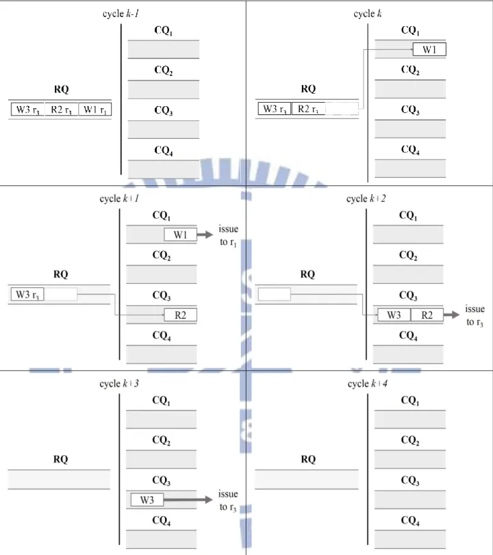
Fig. 5 gives an example of how the memory commands are transferred from the RQ to the CQs when the throttling mechanism is employed. In Fig. 5, each rectangle represents a memory command. The access type of each command is denoted by R (read) or W (write), followed by an index number and the target rank of the command. The index numbers are assigned to each memory command according to the time they entered the RQ. The command that enters the RQ
14
earlier is represented by a smaller index number. For the example shown in Fig. 5, the DRAM is assumed to have four ranks, which are denoted as r1, r2, r3, and r4. Correspondingly, there are
four CQs in the memory controller. Suppose that the throttle delay is reached at cycle k. For simplicity, we denote the ith rank as ri in Fig. 5 as well as in the remainder of this thesis.
As shown in Fig. 5, three commands W1, R2, and W3 are blocked in the RQ during cycle k − 𝑡𝑇𝐷 to cycle k. When the throttle delay is reached, the RQ starts sending commands from its front to its end. Each memory command is sent to the CQ according to its target rank. Hence, W1 is first sent to the CQ1, then R2 is sent to the CQ3, W3 is sent to the CQ3 at last. Each
command in the CQ is issued to the corresponding DRAM rank. CQ1 issues W1 to r1 after
receiving W1 from the RQ. Since the CQ issues commands in FIFO order, CQ3 issues R2 to r3
15
Fig. 5 An example of how the blocked memory commands transfer from the RQ to the CQs when the throttle delay is reached in a throttling mechanism.
16
The DRAM supports rank level power-mode control. That is, each rank has two different power mode, the active mode and the low power mode. A rank has to be turned on to the active mode before it is able to process the received commands. When a rank is idle, it can be turned off to the low power mode by the memory controller. The memory controller puts power-up and power-down commands into the CQ to switch the power mode of its corresponding DRAM rank. Switching the power mode of a rank is at the cost of transition delays.
The abbreviations and notations used throughout this thesis are listed in the following Table I and Table II.
Table I
Table of abbreviations
Abbreviation Definition
DRAM dynamic random access memory
DIMM dual-in-line memory module
ACT activate
PRE precharge
CKE clock enable
PCRAM phase change random access memory
RQ reorder queue
CQ command queue
CQi the command queue assigned to rank i
FIFO first-in-first-out
ri rank i
RAW read after write
17 Table II Table of notations
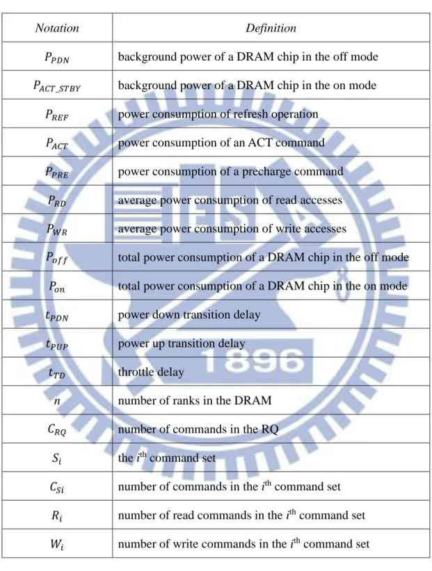
Notation Definition
𝑃𝑃𝐷𝑁 background power of a DRAM chip in the off mode
𝑃𝐴𝐶𝑇_𝑆𝑇𝐵𝑌 background power of a DRAM chip in the on mode
𝑃𝑅𝐸𝐹 power consumption of refresh operation
𝑃𝐴𝐶𝑇 power consumption of an ACT command
𝑃𝑃𝑅𝐸 power consumption of a precharge command
𝑃𝑅𝐷 average power consumption of read accesses
𝑃𝑊𝑅 average power consumption of write accesses
𝑃𝑜𝑓𝑓 total power consumption of a DRAM chip in the off mode
𝑃𝑜𝑛 total power consumption of a DRAM chip in the on mode
𝑡𝑃𝐷𝑁 power down transition delay
𝑡𝑃𝑈𝑃 power up transition delay
𝑡𝑇𝐷 throttle delay
n number of ranks in the DRAM
𝐶𝑅𝑄 number of commands in the RQ
𝑆𝑖 the ith command set
𝐶𝑆𝑖 number of commands in the ith command set
𝑅𝑖 number of read commands in the ith command set
18
2.2 Problem Statement
With the system model described in the previous section, the goal of this thesis is to find a delicate DRAM scheduling scheme that reduces the DRAM power with small system performance degradation for the memory controller. The scheduling scheme includes a throttling mechanism, which controls when the RQ starts sending commands to the CQs. The scheme also contains a scheduling policy for the scheduler inside the RQ, which is able to reorder the sequence of memory request commands in the RQ. The internal commands such as ACT and PRE are not taken into consideration by the scheduler inside the RQ since they are generated and put to the CQs directly by the memory controller. The scheduling policy should guarantee that the reordered sequence of memory commands are hazard-free. Finally, the scheme is in charge of determining when to turn on and off the DRAM ranks.
By using the throttling mechanism, reordering the memory commands and controlling the power mode of ranks, the goal of the proposed scheme is to reduce the power consumption of the DRAM with minor system performance degradation.
19
Chapter 3
The Proposed Techniques
3.1
Overview
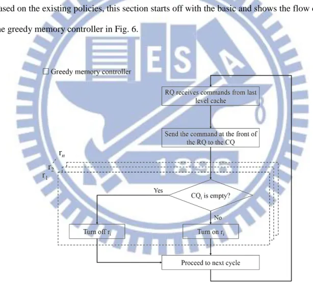
The proposed DRAM power reduction techniques address on lowering DRAM power consumption with slight system performance degradation. Since the proposed techniques are based on the existing policies, this section starts off with the basic and shows the flow chart of the greedy memory controller in Fig. 6.
20
The greedy memory controller employs the greedy power-down policy, which turns off a DRAM rank whenever it is idle. In the greedy power-down policy, an idle rank is turned off even when there are pending commands destine for it in the RQ. The greedy memory controller does not employ the throttling mechanism. Therefore, whenever the RQ is not empty, a single memory command is sent from the RQ to the corresponding CQ every cycle.
As shown in Fig. 6, at any given cycle, the memory commands from the last level cache are pushed to the end of the RQ. The memory controller checks the state of each rank and turns off the ranks that are idle. After turning off idle ranks, the memory controller send the command at the front of the RQ to its corresponding CQ. Finally, the memory control checks each CQ to see if they are empty. If CQi is not empty, the memory controller turns on ri and issues the
commands to it.
Since the greedy memory controller turns off an idle rank regardless of the upcoming memory commands in the RQ, the idle rank is turned off even during a short idle period. This results in frequent power mode transition and leads to dramatic system performance degradation caused by the power mode transition delays [20].
To improve the power reduction and the system performance of the greedy memory controller, the previous work [21] adds the throttling mechanism, the queue-aware power-down policy, and the power-aware memory scheduler to the greedy memory controller. The flow chart of the previous work [21] is shown in Fig. 7.
21
Fig. 7 Flow chart of the memory controller proposed in the previous work [21].
The light-gray rectangles and decision boxes in Fig. 7 are power reduction techniques added by the previous work [21]. The throttling mechanism, which is shown as the first light-gray decision box in the flow chart, blocks memory commands after they are pushed to the RQ until the throttle delay is reached. The blocked commands are not allowed to be sent to the CQ. When the throttle delay is reached, the memory controller clusters the blocked commands into
22
𝑆𝑖. The set of commands destined for the same rank as the command that first entered the RQ
are moved to the front of the RQ, and so on. The memory controller then checks each command set, if there is command in 𝑆𝑖, all the commands in 𝑆𝑖 are allowed to be sent to the CQ. The memory controller then sends command at the front of the RQ to the corresponding CQ. At the end of each cycle, the memory checks each CQ to see if there is commands in it. If CQi is empty,
the memory controller sends a power-down command to ri, which turns ri off.
To sum up, the techniques proposed in the previous work [21] improves both power reduction and system performance from the greedy memory controller. The power-aware memory scheduler in the previous work clusters commands according to their target ranks. This forces the DRAM to concentrate on accessing a certain rank for a period of time, allowing other ranks to be turned off. The queue-aware power-down policy checks the upcoming commands in the CQ before turning off a rank, which prevents a rank to be turned off during a short idle period. When a rank is turned off, the throttling mechanism assures that the rank stays in the low power mode for a long period of time.
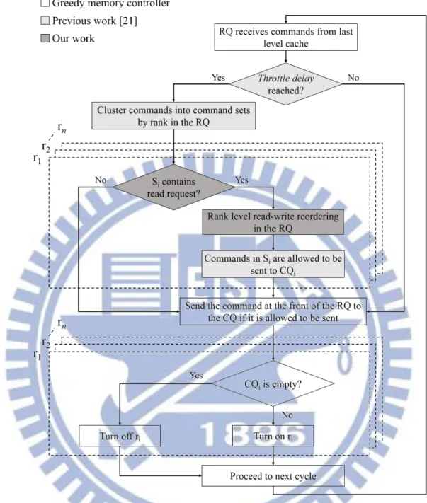
However, the previous work [21] does not maximize the capability of the memory controller. Moreover, it does now take into consideration that the read request are more critical to the system performance than the write requests. Utilizing this fact, this thesis proposes the read-write aware throttling and the rank level read-write reordering techniques to modify the previous work [21]. The flow chart of the memory controller that employs the proposed techniques is shown in Fig. 8.
23
Fig. 8 Flow chart of the memory controller employing the proposed techniques.
Based on the previous work [21], the dark-gray rectangle and box in Fig. 8 are the techniques proposed in this thesis, where the decision box is the read-write aware throttling and the rectangle is the rank level read-write reordering.
The read-write aware throttling mechanism, which is depicted by the dark-gray decision box, checks for the existence of read commands in each command set. Instead of allowing all the nonempty command sets to be sent to the CQs, only the command sets containing read
24
requests are allowed to be sent to the CQs and only their target ranks are turned on. The other ranks, including ranks with write requests pending in the RQ, stay in the low power mode for another throttle delay to reduce the DRAM power consumption.
The dark-gray rectangle shows that the command sets are reordered by the rank level read-write reordering before they are sent to the CQs. The read requests in each command set get higher priorities than the write requests. The commands with higher priorities enter the CQs earlier. Since the CQ issues commands to the DIMM in a FIFO order, the read requests reach their target rank as soon as possible. This makes read requests, which are critical to system performance, to be served by the DIMMs earlier and thus the system performance degradation caused by the throttling mechanism is relieved.
For simplicity, the following notations are used in this thesis. Suppose that there are n
ranks in the DRAM. There is one RQ and n CQs, 𝐶𝑄1, 𝐶𝑄2⋯ 𝑎𝑛𝑑 𝐶𝑄𝑛, inside the memory
controller. The number of commands blocked inside the RQ is denoted as 𝐶𝑅𝑄. Inside the RQ,
commands destined for r1, r2… and rn are clustered into command sets 𝑆1, 𝑆2, ⋯ , 𝑎𝑛𝑑 𝑆𝑛
respectively. The notation 𝐶𝑆𝑖 represents the number of commands in the command set 𝑆𝑖. For each command set 𝑆𝑖, 𝑅𝑖 denotes the number of read commands, while 𝑊𝑖 denotes the number of write commands in it. Therefore, it is clear that we can write the relation between these notations as:
𝐶𝑅𝑄 = ∑ 𝐶𝑆𝑖 𝑛 𝑖=1 = ∑(𝑅𝑖 + 𝑊𝑖) 𝑛 𝑖=1 (3) Using these notations, the detail of the read-write aware throttling mechanism and the rank level read-write reordering are described in the following sections.
25
3.2
Read-Write Aware Throttling
The read-write aware throttling mechanism determines if a rank should be turned on whenever the throttle delay is reached. It checks on each command set 𝑆𝑖, which is composed of memory commands destined for ri in the RQ, to see whether the condition 𝑅𝑖 = 0 is true. If
the condition is satisfied, ri is turned off and all the commands in 𝑆𝑖 remain in the RQ for
another throttle delay. On the other hand, if the condition is not satisfied, ri is turned on and all
the commands in 𝑆𝑖 are allowed to be sent to CQi.
The read-write aware throttling utilizes the fact that read requests affect system performance more than write requests [26]. It is performed on rank level and checks the existence of critical read requests in every command set whenever the throttle delay is reached. If a read request appears in a command set, the memory controller sets the target rank of this command set to urgent. Ranks with no pending read requests are set to trivial. All the commands destined for an urgent rank are allowed to be sent to the corresponding CQ, while other commands remain in the RQ for another throttle delay. This allows the memory controller to only turn on the urgent ranks and keep the trivial ranks in the low power mode, contributing to a large DRAM power saving.
To better understand how the read-write aware throttling mechanism works, we give a simple example. Suppose that there are four ranks in the DRAM. At a certain point, the throttle delay is reached and the memory commands are blocked inside the RQ, as shown in the left part of Fig. 9. Before sending the commands to the CQs, the commands are first clustered into command sets according to their target ranks. The set of commands destined for the same rank as the command enters the RQ first are reordered to the front. The set of commands destined for the same rank as the command that sits right after the command set at the front is reordered to second to the front, and so on. The order of the commands within the same command set remains the same, the command that enters the RQ earlier is closer to the front of the command
26
set. The request command sequence after clustering is shown in the right part of Fig. 9, and the pseudo code of clustering command sets is given below Fig. 9. In the pseudo code, the DRAM is assumed to have n ranks and 𝑐𝑚𝑑𝑗 represents the command in the jth slot in the RQ. The action insert in line 8 reorders a command to the 𝑐𝑚𝑑𝑆𝑒𝑡𝑀𝑎𝑟𝑘[𝑖]th slot and pushes all the commands behind it one slot towards the end of the RQ.
Fig. 9 An example of how commands blocked in the RQ are clustered into command sets.
function ClusterCommandSets( ):
1. for 𝑙 ← 1 to 𝑛 do
2. 𝑐𝑚𝑑𝑆𝑒𝑡𝑀𝑎𝑟𝑘[𝑙] ← −1
3. for 𝑗 ← 1 to 𝐶𝑅𝑄 do
4. // Let the target rank of 𝑐𝑚𝑑𝑗 be 𝑖
5. if 𝑐𝑚𝑑𝑆𝑒𝑡𝑀𝑎𝑟𝑘[𝑖] = −1 then 6. 𝑐𝑚𝑑𝑆𝑒𝑡𝑀𝑎𝑟𝑘[𝑖] ← 𝑗 + 1 7. else 8. insert 𝑐𝑚𝑑𝑗 to 𝑐𝑚𝑑𝑆𝑒𝑡𝑀𝑎𝑟𝑘[𝑖] 9. for 𝑘 ← 1 to 𝑛 do 10. if 𝑐𝑚𝑑𝑆𝑒𝑡𝑀𝑎𝑟𝑘[𝑘] > 𝑐𝑚𝑑𝑆𝑒𝑡𝑀𝑎𝑟𝑘[𝑖] then 11. 𝑐𝑚𝑑𝑆𝑒𝑡𝑀𝑎𝑟𝑘[𝑘] ← 𝑐𝑚𝑑𝑆𝑒𝑡𝑀𝑎𝑟𝑘[𝑘] + 1 12. 𝑐𝑚𝑑𝑆𝑒𝑡𝑀𝑎𝑟𝑘[𝑖] ← 𝑐𝑚𝑑𝑆𝑒𝑡𝑀𝑎𝑟𝑘[𝑖] + 1
27 From Fig. 9, we can see that:
{
𝐶𝑆1 = 5, 𝑅1 = 1, 𝑊1 = 4
𝐶𝑆2 = 1, 𝑅2 = 0, 𝑊2 = 1 𝐶𝑆3 = 2, 𝑅3 = 1, 𝑊3 = 1 𝐶𝑆4 = 0, 𝑅4 = 0, 𝑊4 = 0
The read-write aware throttling then checks for the command sets containing no read request commands. Since the command set 𝑆4 has no commands in it, its target rank r4 is
considered to be trivial and is turned off to save power. The command set 𝑆2 contains no read requests and thus its target rank r2 is also considered trivial and is turned off. All the commands
inside 𝑆2 are kept blocked in the RQ for another throttle delay. The ranks r1 and r3 are
considered urgent because there are read requests in 𝑆1 and 𝑆3. Therefore, commands in 𝑆1 and 𝑆3 are allowed to be sent to 𝐶𝑄1 and 𝐶𝑄3, respectively. The memory controller turns on r1 and r3 to process the commands in 𝑆1 and 𝑆3.
The pseudo code of the read-write aware throttling, is given as below. The function ReadWriteReorder in line 8 will be explained in the next section.
28
In implementation, a one-bit register is used for each command set to detect the existence of read commands whenever a new command enters the RQ. Therefore, the complexity of this procedure is lower than the pseudo code since the if condition in line 5 in the pseudo code is replaced by the registers.
1. if 𝑡ℎ𝑟𝑜𝑡𝑡𝑙𝑒𝑑𝐶𝑦𝑐𝑙𝑒𝑠 = 𝑡𝑇𝐷 then
2. ClusterCommandSets( )
3. for each command set 𝑆𝑖 do
4. 𝑢𝑟𝑔𝑒𝑛𝑡𝑅𝑎𝑛𝑘 ← 𝑓𝑎𝑙𝑠𝑒
5. if 𝑅𝑖 ≠ 0 then
6. 𝑢𝑟𝑔𝑒𝑛𝑡𝑅𝑎𝑛𝑘 ← 𝑡𝑟𝑢𝑒
7. if urgentRank is true then
8. ReadWriteReorder(𝑆𝑖)
9. allow all the commands in 𝑆𝑖 to be sent to 𝐶𝑄𝑖
10. 𝑡ℎ𝑟𝑜𝑡𝑡𝑙𝑒𝑑𝐶𝑦𝑐𝑙𝑒𝑠 ← 0
11. else
12. 𝑡ℎ𝑟𝑜𝑡𝑡𝑙𝑒𝑑𝐶𝑦𝑐𝑙𝑒𝑠 ← 𝑡ℎ𝑟𝑜𝑡𝑡𝑙𝑒𝑑𝐶𝑦𝑐𝑙𝑒𝑠 + 1
10. send the command at the front of the RQ to the corresponding CQ if it is allowed to be sent
11. for each command queue 𝐶𝑄𝑖 do
12. if 𝐶𝑄𝑖 is not empty then
13. turn on ri
14. else
29
3.3 Rank Level Read-Write Reordering
The rank level read-write reordering is a scheduling policy for the command sets containing read requests in the RQ. It gives read requests higher priority than write requests. The commands in a command set are sent to the CQ in descending order of priority. Since the CQ issues commands to the DIMM in FIFO order, read requests are issued to the DIMM prior to write requests. This forces the DIMM inside the DRAM to process read requests, which are critical to system performance, as soon as possible. The rank level read-write reordering effectively relieves the system performance degradation caused by the DRAM power management policy.
The system performance degradation is greatly relieved if the read requests are sent to the CQ prior to all the write requests. However, reordering memory commands blindly can lead to a data hazard issue since the memory commands are no longer handled by the DIMM in the same order as the processors sent out. If a read request enters the RQ after a write request and they are both destined for a same address, a read-after-write (RAW) data hazard occurs if the DIMM returns data for this read request prior to the write request. To avoid RAW hazard, the rank level read-write reordering performs a check before reordering. For each read request in the a command set, the rank level read-write reordering checks all the write requests in the same command set that entered the RQ earlier than this read request. If one or more write requests target to the same address as the read request does, they are combined in their original order to form a command group. All the command groups are then reordered to preserve the FIFO order of the read request in each command group.
An example is given in Fig. 10, where each rectangle represents a memory command with its access type denoted by W (Write) or R (Read) followed by an index number and the target address of the command. The index numbers are assigned to each memory command according the time they entered the RQ. The command that enters the RQ earlier gets a smaller index
30
number. Fig. 10 illustrates how the commands in a command set 𝑆1 is combined into command
groups and reordered.
Fig. 10 An example of how commands in a given command set S1 are combined into
command groups and then reordered.
As shown in Fig. 10, the rank level read-write reordering checks 𝑆1 for read requests. Command R5 is first found, and the rank level read-write reordering search through W1 to W4 to find that W2 and W4 have the same target address as R5. Therefore W2, W4, and R5 and combined into a command group, and the order of these three commands are preserved inside the command group. The rank level read-write reordering then find R6 and W3, which has the same target address as R6. W3 and R6 are thus combined into a command group. Since R5 enters the 𝑆1 before R6, the command group containing R5 is placed in front of the command group containing R6. Commands that are not in any command group are placed in FIFO order behind the last command group.
After combining command groups and reordering, the reordered command sets are sent to the CQs. The target ranks of these command sets are turned on to process these command. It is switched back to the low power mode once all the commands are finished and is kept in the low power mode until the throttle delay is once again reached.
31
The pseudo code of the rank level read-write reordering is given below. In the pseudo code, the command set 𝑆𝑖 is assumed to have 𝐶𝑆𝑖 commands and notations 𝑐𝑚𝑑𝑗 and 𝑐𝑚𝑑𝑘 represent the jth and kth command in the command set, respectively. Notice that in line 6 and line 9, the action insert reorders the command to the markth slot in the command set. For instance, line 6 moves 𝑐𝑚𝑑𝑘 to the markth slot and all the commands originally sitting in the markth slot to the (𝑘 − 1)th slot are shifted to (𝑚𝑎𝑟𝑘 + 1)th slot to kth slot in order.
As shown in the pseudo code, the rank level read-write reordering checks for read requests among all the commands in a command set from the front to the end of the command set. For each read request found, the rank level read-write reordering search through commands that are in front of the read request and do not belong to any command group. All the commands with the same target address as the read request are combined into a command group.
In implementation, the action insert is provided by the modern memory controller and no extra hardware is required. The address comparing action in line 5 uses a comparator, whose size differs from 1-bit to the length of the memory address. When a small comparator is used, the rank level read-write reordering is more conservative and tends to insert more write requests
function ReadWriteReorder(𝑆𝑖):
input: A command set 𝑆𝑖
1. 𝑚𝑎𝑟𝑘 ← 1
2. for 𝑗 ← 1 to 𝐶𝑆𝑖 do
3. if 𝑐𝑚𝑑𝑗 is a read request then
4. for 𝑘 ← 𝑚𝑎𝑟𝑘 to 𝑗 − 1 do
5. if target address of 𝑐𝑚𝑑𝑘 = target address of 𝑐𝑚𝑑𝑗 then
6. insert 𝑐𝑚𝑑𝑘 to 𝑚𝑎𝑟𝑘
7. 𝑚𝑎𝑟𝑘 ← 𝑚𝑎𝑟𝑘 + 1
8. insert 𝑐𝑚𝑑𝑗 to 𝑚𝑎𝑟𝑘
32
in front of the read requests. The effect on relieving system performance degradation may be slightly weaken if a small comparator is used.
33
3.4 An Example of The Proposed Policy
In the proposed scheduling policy, the rank level read-write reordering is combined with the read-write aware throttling. To understand how the proposed policy works, a complete example is given as follows. Assume that there are four ranks in the DRAM and the throttle delay is reached at cycle k. Suppose that at cycle k, the command pattern in the RQ is as shown in the left part of Fig. 11. The commands are clustered into command sets according to their target ranks, the result is as shown in the right part of Fig. 11. Notice that the command set 𝑆4 contains no commands and is therefore omitted in Fig. 11.
Fig. 11 An example of how the read-write aware throttling clusters commands in the RQ and determines which ranks should be turned on when the throttle delay is reached.
When the throttle delay is reached at cycle k, the read-write aware throttling is first
performed to check on each command set for the existence of read commands. As the result, r1
and r3 are considered urgent, while r2 and r4 are considered trivial. After the read-write aware
throttling, the rank level read-write reordering is performed on command sets 𝑆1 and 𝑆3 before they are sent to CQ1 and CQ3. Using 𝑆1 as an example, Fig. 12 shows how the
34
commands in 𝑆1 are reordered and sent to the CQ. The command at the front of the command
set has the highest priority while the command at the end has the lowest priority. The commands are sent to the CQ in descending order of priority one at a cycle.
Fig. 12 An example of how the commands in a given command set 𝑆1 are reordered by the
rank level read-write reordering and sent to the CQ.
As shown in Fig. 12, rank 1 was originally in the low power mode after all the commands from last throttle period are completed. .When the throttle delay is reached and the command set is formed, the rank level read-write reordering checks through the command set and found that W4 and W7 target to the same address as R8. These three commands are then combined to
form a command group and reordered to the front of 𝑆1. Once the reordering completes, the
commands are sent to 𝐶𝑄1 and rank 1 is turned on. Rank 1 is turned off again when all the
command finishes. The example shows that the rank level read-write reordering forces the DRAM to process read requests as early as possible.
It is noticeable that for an urgent rank ri, all the commands in the command set 𝑆𝑖 are
allowed to be sent to 𝐶𝑄𝑖. Even the write requests whose target addresses are not identical to any read requests are allowed to be sent to the corresponding CQ instead of kept blocked in the RQ. For example, the target addresses of W1 and W6 in Fig. 12 are not the same as R8, and
35
they are still sent to 𝐶𝑄1. The reason is that once a rank is activated, keeping these write requests in the RQ does not contribute to more DRAM power reduction because they will eventually be processed and consumes the same amount of power. Moreover, if these write requests are kept blocked in the RQ until a read requests with the same target address enters the command set, the read request has to wait for these write requests to be completed. This lengthens the latency of the critical read request and has chance to worsen the system performance degradation.
36
Chapter 4
Experimental Results
This chapter demonstrates and analyzes the experimental results to examine the proposed techniques. First, the simulation environment is described. Second, the evaluation results of how each techniques proposed in this thesis work at certain throttle delay are shown and analyzed. Finally, the evaluation on the power and performance trade-off is carried out and the results are analyzed and compared with other works.
4.1 Simulation Environment
The performance of our work is evaluated with Multi2Sim [28], a widely used cycle-accurate system simulator. Multi2Sim provides detailed simulation of single core or multicore processors and gives us the statistics of the system performance. Our evaluation integrates DRAMSim2 [29] into Multi2Sim to obtain more accurate statistics of DRAM, such as the latency of each memory command, DRAM power consumption and power mode transition delays. DRAMSim2 is a cycle-accurate, JEDEC DDRx memory system simulator, which models the memory controller, memory channels, DRAM ranks, and banks. In an evaluation, Multi2Sim runs the benchmark and generates memory commands accordingly. The memory commands are sent to DRAMSim2 and processed by the DRAM that DRAMSim2 models. The evaluation results of Multi2Sim provide the system throughput statistics, while the evaluation results of DRAMSim2 provide the DRAM power consumption.
The baseline system in the simulations uses the ARM Coretex-A9 MPCore [30]. The configuration parameters of ARM Coretex-A9 MPCore are listed in Table III. The baseline system has two-level caches. In order to evaluate our work by comparing to the previous work
37
[21], our simulations use the same cache sizes as in the previous work. The detail parameters of the memory system are presented in Table IV. The main memory used in the evaluation is a DDR2 SDRAM, which is one of the JEDEC standard memory available on market [12].
Table III
Configuration parameters of ARM Cortex A9 [30]
Parameter Value
Number of cores 4
Number of threads per core 1
Technology node 40 nm Operating frequency 2.132 GHz Supply voltage 0.66 V Threshold voltage 0.23 V Decode width 2 Issue width 4 Commit width 4
Number of arithmetic logic units per core 3
Number of multipliers per core 1
Number of floating-point units per core 1
38 Table IV
Memory system parameters
Parameter Value
Size of level 1 data cache per core 32 KB
Set associativity of level 1 data cache per core 4-way
Size of level 1 instruction cache 64 KB
Set associativity of level 1 instruction cache per core 2-way
Size of level 2 cache 2 MB
Set associativity of level 2 cache 8-way
DRAM frequency 533 MHz
Number of DRAM ports 2
DRAM device width 8
Number of DRAM ranks 4
Number of DRAM banks per rank 4
Number of DRAM rows per bank 8192
Number of DRAM columns per bank 4096
Table V
Benchmark combinations of floating-point benchmarks in SPEC CPU2006 [31]
Combination Benchmarks
fp1 410.bwaves 416.gamess 433.milc 434.zeusmp
fp2 435.gromacs 436.cactusADM 437.leslie3d 444.namd
fp3 447.dealII 450.soplex 453.povray 454.calculix
fp4 459.GemsFDTD 465.tonto 470.lbm 481.wrf
The workload for our simulations is the SPEC CPU2006 [31] benchmark suite. The benchmarks in the SPEC CPU2006 suite can be separated into integer benchmarks and floating point benchmarks. The floating point benchmarks have higher memory pressure than integer benchmarks and need more sophisticated power management policies [1][21]. Therefore, the benchmarks used in our simulations are randomly chosen from the floating point benchmarks.
39
For each simulation, a benchmark combination containing four benchmarks is used. Every benchmark in the benchmark combination is assigned to a certain core. The benchmark combinations are listed in Table V. Each benchmark combination is run for five million CPU cycles in our evaluation.
Another workload used in the evaluation is the SPLASH-2 benchmarks [32], which are collected from real applications. Using the dynamic context scheduler provided by Multi2Sim [28], each program in the SPLASH-2 benchmarks forks at most four parallel contexts during runtime. The benchmarks in SPLASH-2 used in the evaluation are listed in Table VI.
Table VI
SPLASH-2 [32] benchmarks used in the evaluation
Benchmark Problem size
Barnes 2048 particles
Cholesky tk14.O
FFT 65536 points
FMM 2048 particles
Radix 256k keys, max-value 524288, radix 4096
The SPEC CPU2006 benchmarks are used in section 4.2 and 4.3, and the SPLASH-2 benchmarks are used in section 4.3. In the evaluation, the power consumption is measured in Watts. The system performance is measured in million instructions per second (MIPS), which represents the throughput of the system. All the results are normalized to the native DRAM, which refers to the DRAM with no power management policy.
40
4.2 Analysis on Different Techniques
Although our work employs both the write aware throttling and the rank level read-write reordering, these two techniques can be employed individually. Therefore, the techniques proposed in this thesis are not only evaluated jointly but also separately to see how they affect the DRAM power consumption and the system performance.
In the evaluation, our work is compared to the previous work and an oracle policy. In the oracle policy, the order of the memory accesses is transparent so that the DRAM ranks can be ideally turned on and off when needed. Furthermore, there is no transition delay and transition power in the oracle policy. The power reduction of the oracle policy is the maximum power reduction possible at zero system performance degradation. The oracle policy does not employ any throttling-based mechanism nor reordering. Therefore, the oracle policy can be viewed as a time-out-zero policy, which turns off a rank at the instant it becomes idle, with perfect pre-wakeup capability that turns a rank back on whenever it receives a command.
The benchmark combinations listed in Table V are used in this evaluation. The throttle delay for our work and the previous work is set to 400 CPU cycles, at which both our work and the previous work achieve good power reduction with acceptable system performance degradation. The effect of different throttle delays is analyzed later. The evaluation results of all four benchmark combinations are shown in Fig. 13.
41
(a) DRAM power reduction percentage
(b) Normalized system performance
42
The evaluation results show that when the read-write aware throttling is employed alone, it reduces the DRAM power consumption 10%~15% more than the previous work but causes around 1% more system performance degradation. The reason is that the read-write aware throttling puts a rank into the low power mode until it receives read requests. However, when the rank is turned back on to handle the read requests, there are many write requests waiting to be processed. Without the rank level read-write reordering, the read requests have to wait until all the write requests that enters the queue before them are completed. The system performance is degraded since the critical read requests have to wait for a long time.
On the other hand, when the read-write reordering is used alone with the basic throttling mechanism as in the previous work [21], it improves the system performance by around 1% but the DRAM power consumption remains the same as the previous work [21]. This is because that the rank level read-write reordering only forces the DRAM to process read requests as early as possible and does not create extra power down opportunity.
By combining these two techniques, our work saves 10%~15% more power than the previous work with the same, or even slighter, system performance degradation. More importantly, our work reduces DRAM power consumption to below the oracle solution with 2% of the system performance degradation on average.
The evaluation results show that each technique reacts differently to different benchmark combinations. Since the proposed techniques take into consideration that read requests and write requests are not equally critical to the system performance, the number of requests contained in a benchmark is essential to the effect of the proposed techniques. Therefore, the read requests percentage of each benchmark combination are listed in Table VII. The read requests percentage is obtained by evaluating each benchmark combination with the native DRAM and is calculated by dividing the number of read requests into the total number of memory requests commands.
43 Table VII
Read requests percentage of each benchmark combination
Benchmark combination Read requests percentage
fp1 6.76%
fp2 17.74%
fp3 55.27%
fp4 20.14%
Table VII shows that most of the read requests are completed in the cache, and the read requests that send down to the DRAM is less than write requests. It is obvious that fp3 is the most read intensive benchmark combination, while the fp1 is the least read intensive one. The read intensity of different benchmark combination reflects on the power reduction in the evaluation results. The read-write aware throttling works very well on fp1, which has a weak read intensity, due to the fact that most of the time there are only write requests blocked in the RQ and DRAM ranks can be turned off. On the other hand, the strong read intensity of fp3 limits the effect of the read-write aware throttling since it is less likely for a rank to only receive write request in a throttle period and thus cannot be turned off. Nevertheless, our work still manages to save 5% more DRAM power consumption with slightly better system performance than the previous work [21].
As mentioned in section 1.2, the DRAM power can be partitioned into several parts, including background power, active power, precharge power, read power, write power, and the refresh power. To further analyze the evaluation results, Fig. 14 shows these detail power consumptions obtained from the evaluation and compare them to the power consumption of the native DRAM. In Fig. 14, the ACT/PRE power consumption represents the sum of active power and precharge power, while the Read/write burst power represents the sumation of read power and write power. Notice that the refresh power is omitted because the DRAM is refreshed
44
periodically and the evaluation runs the benchmark for a fixed CPU cycle period, the refresh power consumptions for different techniques are the same.
(a) Background power consumptions of different techniques
45
(c) Read/write burst power consumptions of different techniques
Fig. 14 The background power, ACT/PRE power, and the read/write power consumptions of different techniques.
The results in Fig. 14 show that the DRAM power consumption is dominated by the background power since the main memory accesses are sparse in the evaluation. Therefore, the throttling-based mechanism is used to turn off idle ranks, and the background power consumption of DRAM is greatly reduced. In addition, the read-write aware throttling creates longer idle period for a rank to be turned off and thus reduces 10%~45% more of the background power against the previous work [21]. The ACT/PRE power consumptions and the read/write burst power consumptions show that the read-write aware throttling cuts down the number of returned commands because the DRAM ranks are in the low power mode for a long period. However, when the read-write aware throttling releases the blocked commands from the RQ to the CQ, it forces the DRAM to focus on accessing the active rank.
It is noticeable that the read/write burst power consumption of our work on fp1 is low. It is because that fp1 has a weak read intensity. When the memory controller finally receives a
46
read request and turns on a rank, there are many pending write requests targeting that rank, which are blocked by the read-write aware throttling. As the result, in a command group formed by rank level read-write reordering, there are many write requests in front of the read request. Once the rank is activated, it takes a long time processing the pending write requests before it becomes available to process the critical read request. The system performance is thus harmed and fewer main memory commands are completed within the same simulation period. Therefore, the read/write burst power consumption is lower than other techniques.
![Fig. 7 Flow chart of the memory controller proposed in the previous work [21].](https://thumb-ap.123doks.com/thumbv2/9libinfo/8380381.178159/29.892.163.752.121.861/fig-flow-chart-memory-controller-proposed-previous-work.webp)